 | –≠–ª–µ–∫—Ç—Ä–æ–Ω–Ω—ã–π –∫–æ–º–ø–æ–Ω–µ–Ω—Ç: FA5301BP | –°–∫–∞—á–∞—Ç—å:  PDF PDF  ZIP ZIP |
FA5301BP(N)
1
FA5301BP(N)
s
Description
The FA5301BP(N) is a bipolar IC containing basic circuits
necessary for PWM-type switching power supply control.
This IC switches an external transistor according to external
synchronizing pulses.
s
Features
∑ External synchronization input terminal
∑ Wide supply voltage range (V
CC
=7 to 22V)
∑ Open-collector output
∑ Soft-start from standby mode
∑ Double protection of output transistor by overcurrent limiting
and cutoff functions
∑ Output ON/OFF control function
∑ Not many external discrete components needed
s
Applications
∑ Switching power supply for general equipment
(Optimum for TV, display, and other monitor devices)
s
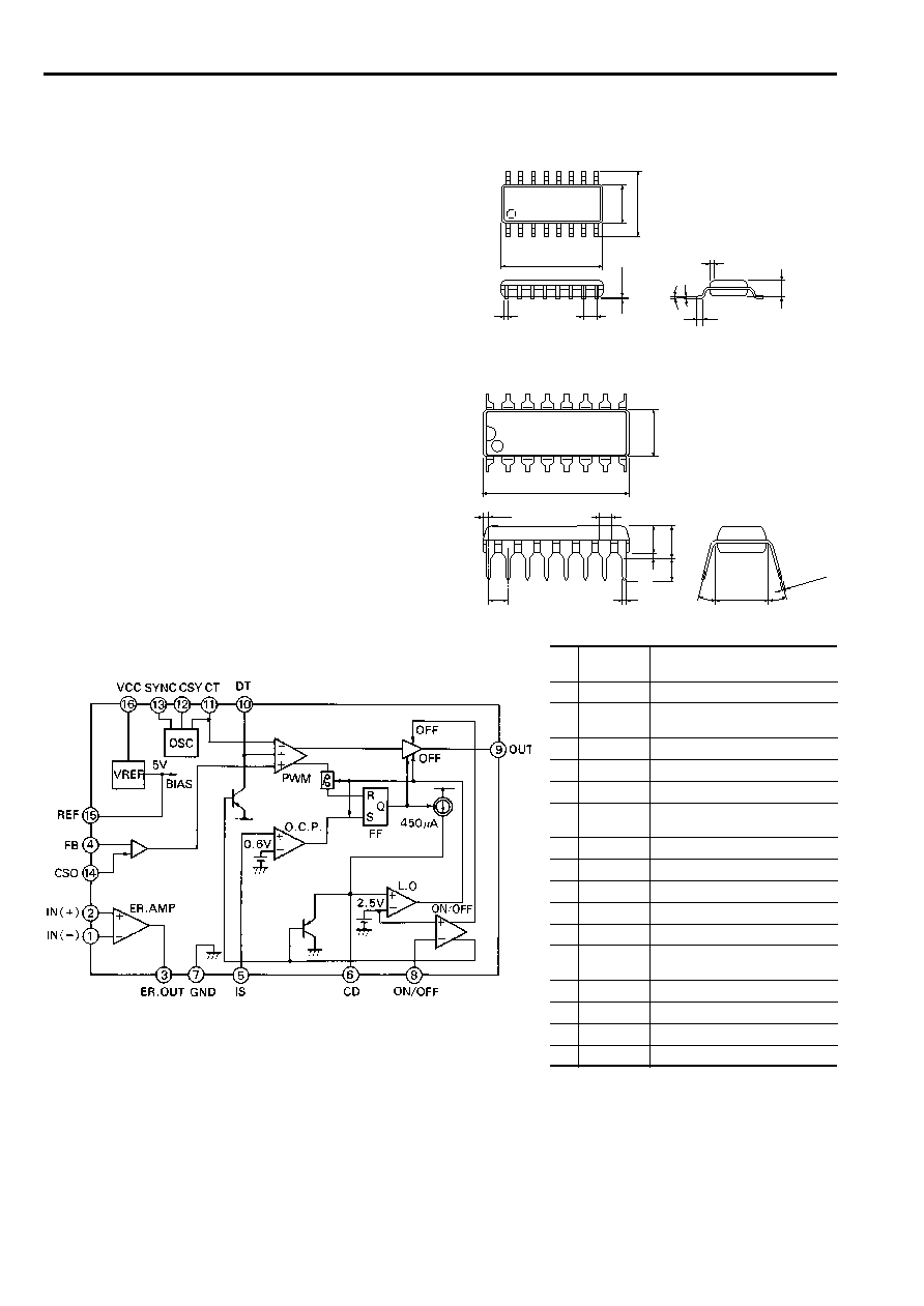
Dimensions, mm
SOP-16
DIP-16
s
Block diagram
1
16
9
8
19.4
6.5
7.6
3.4
4.3max
1.5
0.81
3.1min
0.2min
0~15∞
0~15∞
0.5
±
0.1
2.54
±
0.25
0.3
+0.1
≠0.05
Bipolar IC
For Switching Power Supply Control
1
8
9
16
0.65
0.33
0~8∞
1.27
±
0.2
6.0
±
0.2
3.9
±
0.1
1.65
±
0.1
0.18
±
0.07
0.42
±
0.07
9.9
±
0.1
0.2
Pin
Pin
Description
No.
symbol
1
IN (≠)
Inverting input to error amplifier
2
IN (+)
Non-inverting input to error
amplifier
3
ER.OUT
Error amplifier output
4
FB
Feedback input
5
IS
Overcurrent detection
6
CD
Overcurrent cutoff delay
capacitor
7
GND
Ground
8
ON/OFF
Output ON/OFF control
9
OUT
Output
10
DT
Dead time adjustment
11
CT
Oscillator timing capacitor
12
CSY
External synchronizing signal
detection capacitor
13
SYNC
External synchronization input
14
CSO
PWM soft-start capacitor
15
REF
Reference voltage output (5V)
16
VCC
Power supply

FA5301BP(N)
2
s
Absolute maximum ratings
Item
Symbol
Rating
Unit
V
CC
22
V
V
O
22
V
I
OM
5
mA
V
I
5
V
V
IS
20
V
V
FB
20
V
V
ON/OFF
6
V
V
SYNC
6
V
P
d
1000 (DIP-16) *
1
mW
400 (SOP-16) *
2
T
opr
≠20 to +85
∞
C
T
stg
≠40 to +150
∞
C
Supply voltage
Output voltage
Error amplifier output
current
Error amplifier input
voltage
Overcurrent detection
terminal input voltage
Feedback terminal input voltage
Output ON/OFF terminal
input voltage
Synchronizing terminal
input voltage
Total power dissipation
Operating temperature
Storage temperature
Notes:
*
1
Derating factor Ta > 25
∞
C : 10.0mW/
∞
C (on PC board)
*
2
Derating factor Ta > 25
∞
C : 4.0mW/
∞
C (on PC board)
s
Recommended operating conditions
Item
Symbol
Min.
Max.
Unit
Supply voltage
V
CC
7
20
V
Error amplifier input voltage
V
I
0
V
REF
-2
V
Output current
I
O
20
mA
Error amplifier feedback resistor
R
NF
33
k
Oscillator timing capacitor
C
T
100
10,000
pF
Oscillator timing resistor
R
T
8.2
220
k
Free run oscillation frequency
f
OSC
1
200
kHz
Synchronized frequency
f
SYNC
1
200
kHz
Frequency ratio
CSY
=OV ≠35
≠5
%
f
OSC
≠
f
SYNC
*
3
f
SYNC
≠30
+10
%
CSY
:
C
apacitor
is connected
to GND
*
3
Consider the tolerance of
fosc ≠ f
SYNC
f
SYNC
s
Electrical characteristics (Ta = 25
∞
C, V
CC
= 9V, R
T
= 47k
, C
T
= 1000pF)
Reference voltage section
Item
Symbol
Test condition
Min.
Typ.
Max.
Unit
Output voltage
V
REF
I
OR
= 1mA
4.75
5.00
5.25
V
Line regulation
L
INE
V
CC
= 8 to 20V
10
25
mV
Load current regulation
L
OAD
I
OR
= 0.1 to 2mA
10
25
mV
Output voltage variation by temperature fluctuation
V
TC1
Ta
= ≠20 to +25
∞
C
1
%
V
TC2
Ta
= +25 to +85
∞
C
1
%
Output current at output short-circuit
I
OS
25
mA
Oscillator section
Item
Symbol
Test condition
Min.
Typ.
Max.
Unit
Oscillation frequency
f
OSC
C
T
= 1,000pF,
R
T
= 47k
20
21
22
kHz
Frequency variation by line voltage fluctuation
f
dV
V
CC
= 8 to 20V
2
%
Frequency variation by temperature fluctuation
f
dt1
Ta
= +25 to ≠20
∞
C
≠2
+2
%
f
dt2
Ta
= +25 to +85
∞
C
≠2
+2
%
Input current to synchronizing signal terminal
I
SYNC1
V
SYNC
= 1V
300
600
µ
A
I
SYNC2
V
SYNC
= ≠0.5V
≠60
≠300
µ
A
Input current to synchronizing signal detection terminal
I
CSY1
Pin 12 = 0V,
V
SYNC
= ≠0.5V
≠65
≠130
≠260
µ
A
I
CSY2
Pin 12 = 1V,
V
SYNC
= 1V
200
400
µ
A
Threshold voltage of synchronizing signal detection terminal
V
TH CSY
0.7
1.0
V
Error amplifier section
Item
Symbol
Test condition
Min.
Typ.
Max.
Unit
Input offset voltage
V
IO
≠10
10
mV
Input bias current
I
I
1
µ
A
Common-mode input voltage
V
CM
0
V
REF
≠2 V
Open-loop voltage gain
A
V
70
95
dB
Unity-gain bandwidth
G
B
0.8
MHz
Common-mode signal rejection ratio
CMRR
80
dB
Maximum output voltage
V
OM+
I
OM
= ≠50
µ
A
4
V
V
OM≠
I
OM
= 50
µ
A
0.5
V
Output sink current
I
OM≠
V
OM
= 1V
170
240
µ
A

FA5301BP(N)
3
PWM comparator section
Item
Symbol
Test condition
Min.
Typ.
Max.
Unit
Input bias current (Pin 4)
I
BFB
V
FB
= 1V
≠2.0
≠10.0
µ
A
Input threshold voltage (Pin 4)
V
TH0
Duty cycle = 0%
3.3
V
V
TH100
Duty cycle = 100%
0.2
V
Soft-start signal pin input current
I
CSO
Pin 14 = 3V,
V
FB
= 0V
2.0
10.0
µ
A
Dead time adjustment circuit section
Item
Symbol
Test condition
Min.
Typ.
Max.
Unit
Input bias current
I
BDT
Pin 10 = 1V
≠0.5
≠5
µ
A
Input threshold voltage
V
TH DT0
Duty cycle = 0%
3.2
V
V
TH DT100
Duty cycle = 100%
0.1
V
Reset saturation voltage
V
SAT RS
Pin 10 = ≠100
µ
A
0.25
0.8
V
Overcurrent limiting circuit section
Item
Symbol
Test condition
Min.
Typ.
Max.
Unit
Input bias current (Pin 5)
I
BIS
V
IS
= 0.3V
≠1
µ
A
Input threshold voltage (Pin 5)
V
TH IS
0.5
0.6
0.7
V
Source current of overcurrent cutoff terminal
I
O CD
Pin 6 = 0V,
V
IS
= 1V
≠450
≠700
µ
A
Latch-mode threshold voltage
V
TH LA
1.8
2.2
2.6
V
Reset saturation voltage (Pin 6)
V
SAT RS
Pin 6 = 100
µ
A,
V
IS
= 0V
0.75
1.0
V
Output section
Item
Symbol
Test condition
Min.
Typ.
Max.
Unit
Output leakage current
I
LEAK
V
O
= 22V, output OFF
10
µ
A
L-level output voltage
V
OL
I
O
= 10mA
0.4
0.7
V
Output sink current limit
I
SINK
V
O
= 3V
25
40
55
mA
Output ON/OFF control circuit section
Item
Symbol
Test condition
Min.
Typ.
Max.
Unit
Input bias current (Pin 8)
I
BON
Pin 8 = 0V
≠60
≠300
µ
A
OFF-to-ON threshold voltage
V
TH ON
OFF
ON
2.13
2.50
2.87
V
ON-to-OFF threshold voltage
V
TH OFF
ON
OFF
1.96
2.30
2.64
V
Voltage hysteresis
V
HYS
0.2
V
Overall device
Item
Symbol
Test condition
Min.
Typ.
Max.
Unit
Supply current
I
CC LA
R
T
= 47k
, latch mode
8.0
12.0
mA
Operating-state supply current
I
CC AV
R
T
= 47k
, duty cycle = 50%
6.5
9.8
mA

FA5301BP(N)
4
s
Characteristic curves (Ta = 25
∞
C)
Oscillation frequency (f
OSC
) vs. timing
Output duty cycle vs. DT terminal voltage (V
DT
)
resistor resistance (R
T
)
1
7
10
20
50
R
T
[k
]
100
200
500
2200pF
1500pF
1000pF
680pF
470pF
C
T
=100pF
10
5
100
50
fosc [kHz]
1000
500
Output duty cycle vs. FB terminal voltage (V
FB
)
L-level output voltage vs. output sink current (I
SINK
)
Supply current (I
CC
) vs. supply voltage (V
CC
)
Error amplifier frequency (f) vs.voltage gain(Av)/ phase (
)

FA5301BP(N)
5
s
Application circuit
Switching power supply (primary current control and insulated output type)
This circuit uses the following functions.
∑ Horizontal synchronizing function
∑ Overcurrent limiting function
∑ Overcurrent cutoff function
∑ Undervoltage input cutoff function
∑ Soft-start function
Parts tolerances characteristics are not defined in the circuit design
sample shown above. When designing an actual circuit for a product,
you must determine parts tolerances and characteristics for safe and
economical operation.