 | –≠–ª–µ–∫—Ç—Ä–æ–Ω–Ω—ã–π –∫–æ–º–ø–æ–Ω–µ–Ω—Ç: FA5305APS | –°–∫–∞—á–∞—Ç—å:  PDF PDF  ZIP ZIP |

FA5304AP(S)/FA5305AP(S)
1
s
Description
The FA5304AP(S) and FA5305AP(S) are bipolar ICs for
switching power supply control and can directly drive a power
MOSFET. These ICs contain many functions in a small 8-pin
package. With these ICs, a high-performance power supply
can be created compactly because not many external
components are needed.
s
Features
∑ Drive circuit for connecting a power MOS-FET (I
O
=
±
1.5A)
∑ Wide operating frequency range (5 to 600kHz)
∑ Pulse-by-pulse overcurrent limiting function
Positive voltage detection: FA5304AP(S)
Negative voltage detection: FA5305AP(S)
∑ Overload cutoff function (Latch or non-protection mode
selectable)
∑ Output ON/OFF control function by external signals
∑ Overvoltage cutoff function in latch mode
∑ Undervoltage malfunction prevention function (ON at 16V
and OFF at 8.7V)
∑ Error amplifier for control by tertiary winding detection
∑ Low standby current (90
µ
A typ.)
∑ 8-pin package (DIP/SOP)
s
Applications
∑ Switching power supply for general equipment
s
Dimensions, mm
SOP-8
6.05
5.3
8.2
±
0.3
0.4
±
0.1
1.27
±
0.2
0.6
0.20
+0.1
≠0.05
0~10
∞
1
4
8
5
2.0max
DIP-8
Bipolar IC
For Switching Power Supply Control
FA5304AP(S)/FA5305AP(S)
1
8
5
4
9.3
6.5
7.6
3.4
4.5max
1.5
3.0min
0~15∞
0~15∞
0.5
±
0.1
2.54
±
0.25
0.3
+0.1
≠0.05
FA5304AP(S)/FA5305AP(S)
2
s
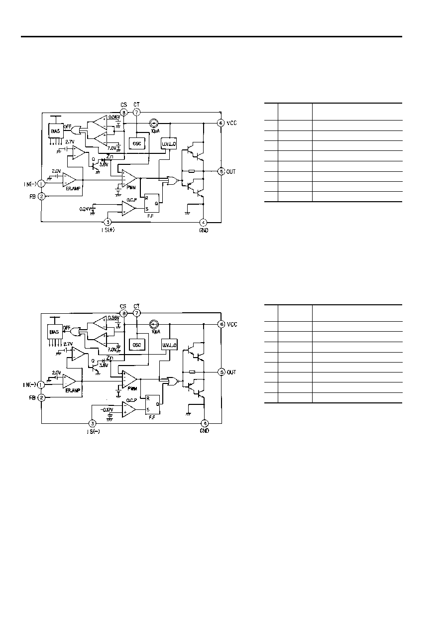
Block diagram
FA5304AP(S)
Pin
Pin
Description
No.
symbol
1
IN (≠)
Inverting input to error amplifier
2
FB
Error amplifier output
3
IS (+)
Overcurrent (+) detection
4
GND
Ground
5
OUT
Output
6
VCC
Power supply
7
CT
Oscillator timing capacitor
8
CS
Soft-start and ON/OFF control
FA5305AP(S)
Pin
Pin
Description
No.
symbol
1
IN (≠)
Inverting input to error amplifier
2
FB
Error amplifier output
3
IS (≠)
Overcurrent (≠) detection
4
GND
Ground
5
OUT
Output
6
VCC
Power supply
7
CT
Oscillator timing capacitor
8
CS
Soft-start and ON/OFF control

FA5304AP(S)/FA5305AP(S)
3
s
Absolute maximum ratings
Common to FA5304AP(S) and FA5305AP(S)
Item
Symbol
Rating
Unit
V
CC
30
V
I
O
±
1.5
A
V
IN
4
V
V
FB
4
V
V
IS
≠0.3 to +4
V
I
CS
2
mA
P
d
800 (DIP-8) *
1
mW
550 (SOP-8) *
2
T
opr
≠30 to +85
∞
C
T
stg
≠40 to +150
∞
C
s
Recommended operating conditions
Common to FA5304AP(S) and FA5305AP(S)
Item
Symbol
Min.
Max.
Unit
Supply voltage
V
CC
10
30
V
Error amplifier feedback resistor
R
NF
100
k
Soft-start capacitor
C
S
0.1
1
µ
F
Oscillation frequency
f
OSC
5
600
kHz
Supply voltage
Output current
Error amplifier input
voltage
Feedback terminal input voltage
Overcurrent detection
terminal input voltage
CS terminal input current
Total power dissipation
(Ta = 25
∞
C)
Operating temperature
Storage temperature
Notes:
*1 Derating factor Ta > 25
∞
C : 8.0mW/
∞
C ( on PC board )
*2 Derating factor Ta > 25
∞
C : 5.5mW/
∞
C ( on PC board )
s
Electrical characteristics (Ta=25
∞
C, V
CC
=18V,fosc=135kHz)
Oscillator section
Common to FA5304AP(S) and FA5305AP(S)
Item
Symbol
Test condition
Min.
Typ.
Max.
Unit
Oscillation frequency
f
OSC
C
T
= 360pF
112
135
148
kHz
Frequency variation 1 (due to supply voltage change)
f
dv
V
CC
= 10 to 30V
±
1
%
Frequency variation 2 (due to temperature change)
f
dT
T
a
= ≠30 to +85
∞
C
±
4
%
Error amplifier section
Common to FA5304AP(S) and FA5305AP(S))
Item
Symbol
Test condition
Min.
Typ.
Max.
Unit
Reference voltage
V
B
1.90
2.00
2.10
V
Input bias current
I
B
V
1
= 2V
≠500
≠50
nA
Open-loop voltage gain
A
V
80
dB
Unity-gain bandwidth
f
T
1.0
MHz
Maximum output voltage (Pin 2)
V
OM+
R
NF
= 100k
2.70
V
V
OM≠
R
NF
= 100k
200
mV
Output source current (Pin 2)
I
MO+
V
OM
= 1V
≠100
≠50
µ
A
Pulse width modulation circuit section
Common to FA5304AP(S) and FA5305AP(S)
Item
Symbol
Test condition
Min.
Typ.
Max.
Unit
Input threshold voltage (Pin 2)
V
TH FBO
Duty cycle = 0%
0.80
1.00
1.20
V
V
TH FBM
Duty cycle =
D
MAX
1.70
1.90
2.10
V
Maximum duty cycle
D
MAX
42
45
50
%
Soft-start circuit section
Common to FA5304AP(S) and FA5305AP(S)
Item
Symbol
Test condition
Min.
Typ.
Max.
Unit
Charge current (Pin 8)
I
CHG
Pin 8 = 0V
≠15
≠10
≠5
µ
A
Input threshold voltage (Pin 8)
V
TH CSO
Duty cycle = 0%
0.80
1.00
1.20
V
V
TH CSM
Duty cycle =
D
MAX
1.70
1.90
2.10
V

FA5304AP(S)/FA5305AP(S)
4
Overcurrent limiting circuit section
Item
Symbol
Test condition
FA5304AP(S)
FA5305AP(S)
Unit
Min.
Typ.
Max.
Min.
Typ.
Max.
Input threshold voltage (Pin 3)
V
TH IS
0.20
0.24
0.28
≠0.20 ≠0.17 ≠0.14 V
Overcurrent detection terminal source current
I
IS
Pin 3 = 0V
≠300
≠200
≠100
≠240
≠160
≠80
µ
A
Delay time
T
PD IS
150
200
ns
Latch-mode cutoff circuit section
Common to FA5304AP(S) and FA5305AP(S)
Item
Symbol
Test condition
Min.
Typ.
Max.
Unit
CS terminal sink current
I
SINK CS
Pin 8 = 6V, Pin 2 = 1V
40
70
150
µ
A
Cutoff threshold voltage (Pin 8)
V
TH CS
6.5
7.0
7.5
V
Overload cutoff circuit section
Common to FA5304AP(S) and FA5305AP(S)
Item
Symbol
Test condition
Min.
Typ.
Max.
Unit
Cutoff threshold voltage (Pin 2)
V
TH FB
2.5
2.7
2.9
V
Undervoltage lock-out circuit section
Common to FA5304AP(S) and FA5305AP(S)
Item
Symbol
Test condition
Min.
Typ.
Max.
Unit
OFF-to-ON threshold voltage
V
TH ON
15.5
16.0
16.5
V
ON-to-OFF threshold voltage
V
TH OFF
8.20
8.70
9.20
V
Voltage hysteresis
V
HYS
7.30
V
Output section
Common to FA5304AP(S) and FA5305AP(S)
Item
Symbol
Test condition
Min.
Typ.
Max.
Unit
L-level output voltage
V
OL
I
O
= 100mA
1.30
1.80
V
H-level output voltage
V
OH
I
O
= ≠100mA,
V
CC
= 18V
16.0
16.5
V
Rise time
tr
No load
50
ns
Fall time
tf
No load
50
ns
Output ON/OFF control circuit section
Common to FA5304AP(S) and FA5305AP(S)
Item
Symbol
Test condition
Min.
Typ.
Max.
Unit
CS terminal source current
I
SOURCE CS
Pin 8 = 0V
≠15
≠10
≠5
µ
A
OFF-to-ON threshold voltage (Pin 8)
V
TH ON
CS pin voltage
0.56
0.76
V
ON-to-OFF threshold voltage (Pin 8)
V
TH OFF
CS pin voltage
0.30
0.42
V
Overall device
Common to FA5304AP(S) and FA5305AP(S)
Item
Symbol
Test condition
Min.
Typ.
Max.
Unit
Standby current
I
CC ST
V
CC
= 14V
90
150
µ
A
Operating-state supply current
I
CC OP
9
15
mA
OFF-state supply current
I
CC OFF
1.1
1.8
mA
Cutoff-state supply current
I
CCL
1.1
1.8
mA
5
FA5304AP(S)/FA5305AP(S)
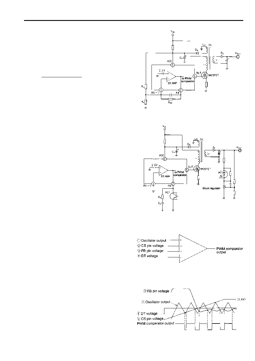
Fig. 1 Configuration with error amplifier
Fig. 2 Configuration with optocoupler (FB pin input)
Fig. 3 PWM comparator
Fig. 4 PWM comparator timing chart
s
Description of each circuit
1. Oscillator (See block diagram on page 8.)
The oscillator generates a triangular waveform by charging
and discharging a capacitor. CT pin voltage oscillates
between an upper limit of approx. 3.0V and a lower limit of
approx. 1.0V. The oscillation frequency is determined by a
external capacitance C
T
connected to CT pin, and
approximately given by the following equation:
..................(1)
The recommended oscillation range is between 5k and
600kHz.
The oscillator output is connected to a PWM comparator.
2. Feedback circuit
Figure 1 gives an example of connection in which built-in error
amplifier is used to couple the feedback signal to IN(-) pin. Let n
2
be the number of turns of secondary winding L
2
and n
3
be the
number of turns of tertiary winding L
3
. V
CC
and Vout are given by
Vcc= 2(V)∑(R
1
+R
2
)/R
2
....................................(2)
V
OUT
(n
2
/n
3
)∑(Vcc+V
D3
)≠V
D2
........................(3)
(where V
D2
and V
D3
are the forward voltage drops across diodes D
2
and D
3
respectively).
Here, the following equation must be satisfied to prevent from
the malfunction of OUT pin at shutdown.
(R1∑R2)/ (R1+R2)
11k
...............................(4)
Figure 2 gives an example of connection in which an
optocoupler is used to couple the feedback signal to the FB
pin. If this circuit causes power supply instability, the frequency
gain can be decreased by connecting R
4
and C
4
as shown in
figure 2. R
4
should be between several tens of ohms to
several kiloohms and C
4
should be between several thousand
picofarads to one microfarads.
3. PWM comparator
The PWM comparator has four inputs as shown in Figure 3.
Oscillator output
x
is compared with CS pin voltage
, FB pin
, and DT voltage
{
. The lowest of three inputs
,
, and
{
is compared with output
x
. If it is lower than the oscillator
output, the PWM comparator output is high, and if it is higher
than the oscillator output, the PWM comparator output is low
(see Fig. 4).
The IC output voltage is high during when the comparator
output is low, and the IC output voltage is low during when the
comparator output is high.
When the IC is powered up, CS pin voltage
controls soft
start operation. The output pulse then begins to widen
gradually. During normal operation, the output pulse width is
determined within the maximum duty cycle (FA5304A,
FA5305A: 45%) set by DT voltage
{
under the condition set
by feedback signal
, to stabilize the output voltage.
C
T
(pF)
f (kH
Z
) =
4.8 ∑ 10
4

6
FA5304AP(S)/FA5305AP(S)
4. CS pin circuit
As shown in Figure 5, capacitor C
S
is connected to the CS pin.
When power is turned on, the constant current source (10
µ
A)
begins to charge capacitor C
S
. Accordingly, the CS pin voltage
rises as shown in Figure 6. The CS pin is connected to an
input of the PWM comparator. The device is in soft-start mode
while the CS pin voltage is between 1.0V and 1.9V common to
FA5304A and FA5305A. During normal operation, the CS pin
is clamped at 3.6V by internal zener diode Zn. If the output
voltage drops due to an overload, etc., the clamp voltage shifts
from 3.6V to 8.0V. As a result, the CS pin voltage rises to 8.0V.
The CS pin is also connected to latch comparator C2. If the pin
voltage rises above 7.0V, the output of comparator C2 goes
high to turn off the bias circuit , thereby shutting the output
down. Comparator C2 can be used not only for shutdown in
response to an overload, but also for shutdown in response to
an overvoltage. Comparator C1 is also connected to the CS
pin, and the bias circuit is turned off and the output is shut
down if the CS pin voltage drops below 0.42V. In this way,
comparator C1 can also be used for output on/off control.
As explained above, the CS pin can be used for soft-start
operation, overload and overvoltage output shutdown and
output on/off control.
Further details on the four functions of the CS pin are given
below.
4.1 Soft start function
Figure 7 shows the soft start circuit. Figure 8 is the soft-start
operation timing chart. The CS pin is connected to capacitor
C
S
. When power is turned on, a 10
µ
A constant-current source
begins to charge the capacitor. As shown in the timing chart,
the CS pin voltage rises slowly in response to the charging
current. The CS pin is connected internally to the PWM
comparator. The comparator output pulse slowly widens as
shown in the timing chart.
The soft start period can be approximately evaluated by the
period ts from the time the IC is activated to the time the output
pulse width widens to 30%. Period ts is given by the following
equation:
t
S
(m
S
) = 160C
S
(
µ
F).................................(2)
Fig. 5 CS pin circuit
Fig. 6 CS pin waveform
Fig. 7 Soft-start circuit
Fig. 8 Soft-start timing chart

7
FA5304AP(S)/FA5305AP(S)
4.2 Overload shutdown
Figure 9 shows the overload shutdown circuit, and Figure 10 is
a timing chart which illustrates overload shutdown operation.If
the output voltage drops due to an overload or short-circuit, the
output voltage of the FB pin rises. If FB pin voltage exceeds
the reference voltage (2.7V) of comparator C3, the output of
comparator C3 switches low to turn transistor Q off. In normal
operation, transistor Q is on and the CS pin is clamped at 3.6V
by zener diode Zn. With Q off, the clamp is released and the
10
µ
A constant-current source begins to charge capacitor C
S
again and the CS pin voltage rises. When the CS pin voltage
exceeds the reference voltage (7.0V) of comparator C2, the
output of comparator C2 switches high to turn the bias circuit
off. The IC then enters the latched mode and shuts the output
down. Shutdown current consumption is 400
µ
A(V
CC
=9V).
This current must be supplied through the startup resistor. The
IC then discharges the MOSFET gates.
Shutdown operation initiated by an overload can be reset by
lowering supply voltage V
CC
below 8.7V or forcing the CS pin
voltage below 7.0V.The period t
OL
from the time that the output
is short-circuited to the time that the bias circuit turns off is
given by the following equation:
t
OL
(m
S
) = 340Cs(
µ
F).........................................(3)
4.3 Overvoltage shutdown
Figure 11 shows the overvoltage shutdown circuit, and Figure
12 is a timing chart which illustrates overvoltage shutdown
operation.
The optocoupler PC1 is connected between the CS and V
CC
pins. If the output voltage rises too high, the PC1 turns on to
raise the voltage at the CS pin via resistor R
6
. When the CS
pin voltage exceeds the reference voltage (7.0V) of
comparator C2, comparator C2 switches high to turn the bias
circuit off. The IC then enters the latched mode and shuts the
output down. The shutdown current consumption of the IC is
400
µ
A(V
CC
=9V). This current must be applied via startup
resistor R
5
.
The IC then discharges the MOSFET gates.
The shutdown operation initiated by an overvoltage condition
can be reset by lowering supply voltage V
CC
below 8.7V or
forcing the CS pin voltage below 7.0V.
During normal operation, the CS pin is clamped by a 3.6V
zener diode with a sink current of 150
µ
A max. Therefore, a
current of 150
µ
A or more must be supplied by the optocoupler
in order to raise the CS pin voltage above 7.0V.
Fig. 9 Overload shutdown circuit
Fig. 10 Overload shutdown timing chart
Fig. 11 Overvoltage shutdown circuit
Fig. 12 Overvoltage shutdown timing chart

8
FA5304AP(S)/FA5305AP(S)
4.4 Output ON/OFF control
The IC can be turned on and off by an external signal applied to
the CS pin.
Figure 13 shows the external output on/off control circuit, and
Figure 14 is the timing chart.
The IC is turned off if the CS pin voltage falls below 0.42V. The
output of comparator C1 switches high to turn the bias circuit
off. This shuts the output down. The IC then discharges the
MOSFET gates.
The IC turns on if the CS pin is opened for automatic soft start.
The power supply then restarts operation.
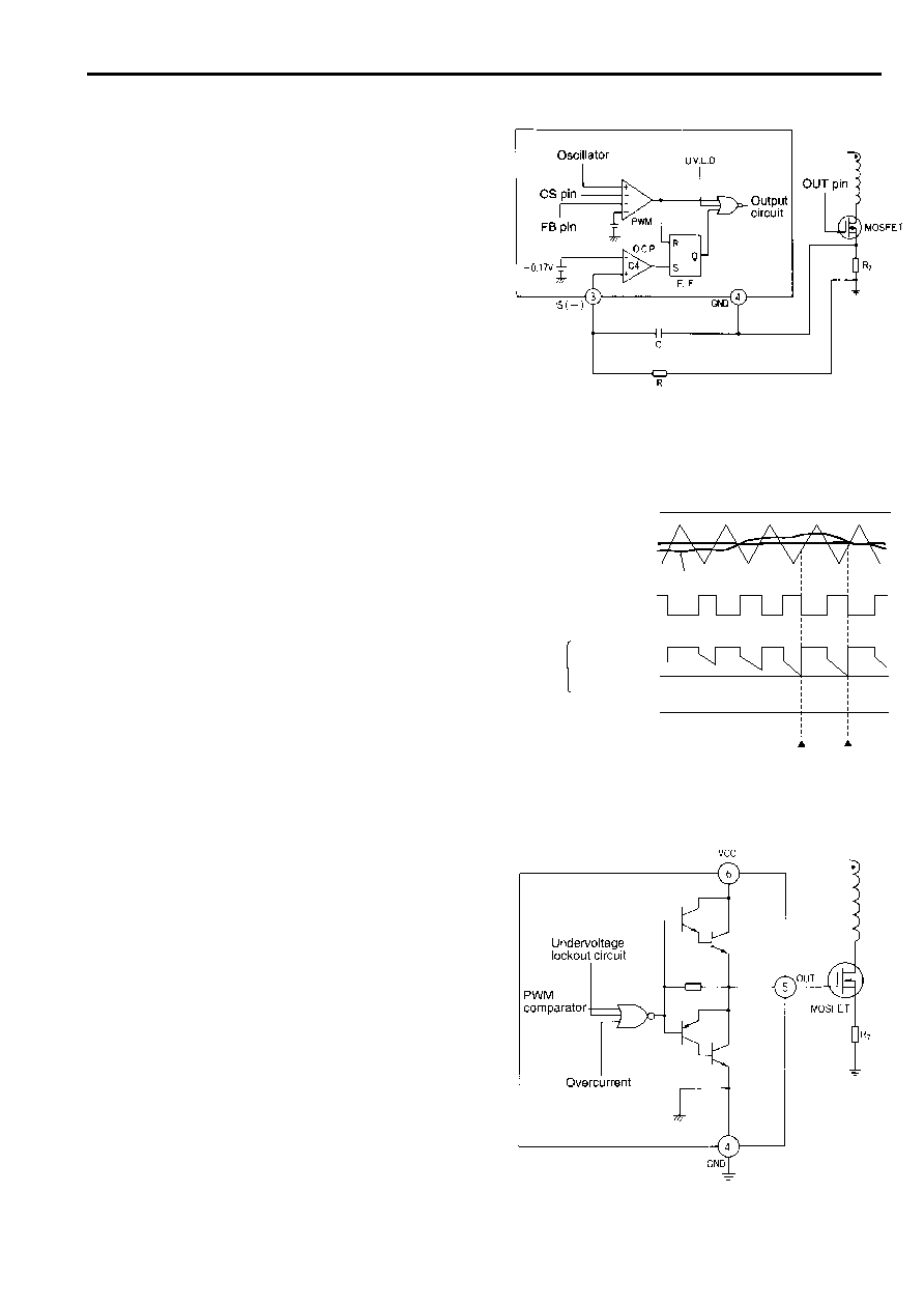
5. Overcurrent limiting circuit
The overcurrent limiting circuit detects the peak value of every
drain current pulse of the main switching MOSFET to limit the
overcurrent.
The detection threshold is
+
0.24V for FA5304A with respect to
ground as shown in Figure 15.
The drain current of the MOSFET is converted to voltage by
resistor R
7
and fed to the IS pin of the IC. If the voltage exceeds
the reference voltage (0.24V) of comparator C4, the output of
comparator C4 goes high to set flip-flop output Q high. The
output is immediately turned off to shut off the current. Flip-flop
output Q is reset on the next cycle by the output of the PWM
comparator to turn the output on again. This operation is
repeated to limit the overcurrent.
If the overcurrent limiting circuit malfunctions due to noise,
place an RC filter between the IS pin and the MOSFET.
Figure 16 is a timing chart which illustrates current-limiting
operations.
Fig. 13 External output on/off control circuit
Fig. 14 Timing chart for external output on/off control
Fig. 16 Overcurrent timing chart for FA5304A
Fig. 15 Overcurrent limiting circuit for FA5304A
9
FA5304AP(S)/FA5305AP(S)
The detection threshold is -0.17v for FA5305A with respect to
ground as shown in Figure 17.
The operation is similar to that of FA5304A except the
threshold is minus voltage compared to that which is plus
voltage for FA5304A.
Figure 18 is a timing chart which illustrates current limiting
operations.
6. Undervoltage lockout circuit
The IC incorporates a circuit which prevents the IC from
malfunctioning when the supply voltage drops. When the
supply voltage is raised from 0V, the IC starts operation with
V
CC
=16.0V.
If the supply voltage drops, the IC shuts its output down when
V
CC
=8.7V. When the undervoltage lockout circuit operates, the
CS pin goes low to reset the IC.
7. Output circuit
As shown in Figure 19, the IC's totem-pole output can directly
drive the MOSFET. The OUT pin can source and sink currents
of up to 1.5A.
If IC operation stops when the undervoltage lockout circuit
operates, the gate voltage of the MOSFET goes low and the
MOSFET is shut down.
Fig. 17 Overcurrent limiting circuit for FA5305A
Fig. 18 Overcurrent timing chart for FA5305A
Fig. 19 Output circuit
CS pin voltage (3.6V)
DT voltage
FB pin voltage
Oscillator output
OUT pin output
H
L
IS ( ≠ ) pin voltage
Comparator C4
Reference
voltage (≠ 0.17V)
Bias voltage
OFF
Overcurrent limiting
Minus
detection

FA5304AP(S)/FA5305AP(S)
10
s
Design advice
1. Startup circuit
It is necessary to start-up IC that the voltage inclination of VCC
terminal "dVcc/dt" satisfies the following equation(4).
dVcc/dt(V/s)>1.8/(Cs(
µ
F)).................................(4)
Cs : capacitor connected between CS terminal and GND
Note that equation (4) must be satisfied in any condition. Also,
it is necessary to keep "latch mode" for overload protection or
overvoltage protection that the current supplied to VCC
terminal through startup resistor satisfies the following
equation(5).
Icc(Lat)>0.4mA for Vcc
9.2V.......................(5)
Icc(Lat): Cutoff-state(=Latch mode) supply current
The detail is explained as follows.
(1) Startup circuit connected to AC line directly
Fig. 20 shows a typical startup circuit that a startup resistor Rc
is connected to AC line directly. The period from power-on to
startup is determined by Rc, R
D
and C
A
. Rc, R
D
and C
A
must
be designed to satisfy the following equations.
dVcc/dt(V/s)=
(1/C
A
) ∑ {(V
AVE
≠Vccon )/R
C
≠Vccon/R
D
≠Iccst} >
1.8/(Cs(
µ
F)).....................................................(6)
Rc(k
)< (V
AVE
≠9.2(V))/{0.4 (mA) + (9.2(V)/R
D
(k
) } ...........(7)
V
AVE
= Vac ∑ 2/
: Average voltage applied to AC line side of Rc
Vac:
AC input effective voltage
Vccon: ON threshold of UVLO, 16.5V(max.)
Iccst:
Standby current, 0.15 mA(max.)
In this method, Vcc voltage includes ripple voltage influenced
by AC voltage. Therefore, enough dVcc/dt required by
equation (6) tend to be achieved easily when Vcc reaches to
Vccon even if Vcc goes up very slowly.
After power-off, Vcc does not rise up because a voltage
applied from bias winding to VCC terminal decreases and the
current flowing R
C
becomes zero, therefore, re-startup does
not occur after Vcc falls down below OFF threshold of UVLO
until next power-on.
Fig. 20 Startup circuit example(1)

FA5304AP(S)/FA5305AP(S)
11
(2) Startup circuit connected to rectified line
This method is not suitable for FA5304A and FA5305A,
especially concerned with re-startup operation just after power-
off or startup which AC input voltage goes up slowly. Fig. 21
shows a startup circuit that a startup resistor R
A
is connected
to rectified line directly.
The period from power-on to startup is determined by R
A
, R
B
and C
A
. R
A
, R
B
and C
A
must be designed to satisfy the
following equations.
dVcc/dt(V/s)=
(1/C
A
)∑{( V
IN
≠Vccon )/R
A
≠ Vccon/R
B
≠Iccst } >
1.8/(Cs(
µ
F))................................................(8)
R
A
(k
)< (V
IN
≠ 9.2(V))/{0.4(mA) + (9.2(V)/R
B
(k
))}..............(9)
V
IN
:
2 ∑(AC input effective voltage)
After power-off, once V
CC
falls down below OFF threshold
voltage, V
CC
rises up again and re-startup occurs while the
capacitor C
1
is discharged until approximately zero because
V
CC
voltage rises up by the current flowing R
A
.
This operation is repeated several times.
After the repeated operation, IC stops in the condition that V
CC
voltage is equal to Vccon
(=ON threshold) because capacitor
C
1
is discharged gradually and the decreased V
CC
inclination
is out of the condition required by equation (4).
After that, re-startup by power-on can not be guaranteed even
when equation (8) is satisfied. The image of that the startup is
impossible is shown in Fig. 22. It is necessary to startup IC
that supply current Icc (startup) to VCC is over 4mA in the
condition of Tj < 100
∞
C during Vcc is kept at Vccon( 16V,
balance state at Vccon after the repeated operation.
Icc (start-up) > 4mA..............................(10)
at Vcc=Vccon, Tj<100
∞
C, after power-off
This balance state that startup is impossible tends to occur at
higher temperature.
If power-on is done when Vcc is not kept at Vccon (for
example: power-off is done and after enough time that C
1
is
discharged until Vcc can not be pulled up to Vccon), the IC can
startup in the condition given by equation(8).
In some cases, such as when the load current of power supply
is changed rapidly, you may want to prolong the hold time of
the power supply output by means of maintaining Vcc over the
off threshold.
For this purpose, connect diode D
4
and electrolytic capacitor
C
4
as shown in Fig. 23. This prolongs the hold time of the
power supply voltage Vcc regardless of the period from power-
on to startup.
Fig. 21 Startup circuit example(2)
Fig. 23 Startup circuit example(3)
Startup is impossible
Power ON
Power OFF
Vccon
Vccoff
Startup is impossible (dVcc/dt <1.8/Cs
just before Vcc reaches Vccon).
Icc>4mA is necessary for startup at
Tj <100
∞
C and dVcc/dt=0.
Fig. 22 Image of Vcc waveform when re-startup is impossible

FA5304AP(S)/FA5305AP(S)
12
2. Disabling overload shutdown function
As shown in Figure 24, connect a 330k
to 470k
resistor
between the CS pin and ground. Then, the CS pin voltage
does not rise high enough to reach the reference voltage
(7.0V) of the latch comparator, and the IC does not enter the
OFF latch mode. With this connection, the overvoltage
shutdown function is not available.
3. Setting soft start period and OFF latch delay
independently
Figure 25 shows a circuit for setting the soft start period and
OFF latch delay independently. In this circuit, capacitance C
S
determines the soft start period, and capacitance C
L
determines the OFF latch delay. If the overload shutdown and
overvoltage shutdown functions raise the CS pin voltage to
around 5V, zener diode Zn becomes conductive to charge C
L
.
The OFF latch delay can be thus prolonged by C
L
.
4. Laying out Vcc and ground lines
Figure 26 and Figure 27 show the recommended layouts of
V
CC
and ground lines. The bold lines represent paths carrying
large currents. The lines must have an adequate thickness.
5. Sink current setting for CS terminal
A sink current to CS terminal must be satisfied the following
condition to prevent from the malfunction which uncontrolled
pulse output generates at OUT terminal when latch-mode
protection should be operated for overvoltage.
150
µ
A < Ics(sink) < 500
µ
A at Vcs= 6.5(V)
Ics(sink): Sink current to CS terminal
Example (for the circuit shown in Fig. 28 )
Ics(sink) = (28(V)≠18(V)≠ 6.5(V))/7.5(k
)
467 (
µ
A) < 500 (
µ
A)
Fig. 25 Independent setting of soft-start period and OFF latch
delay
Fig. 26 Vcc line and ground line for FA5304A
CS
VCC
7.5k
18V Zener diode
Under 500
µ
A
Fig. 24 Disabling overload shutdown function
Fig. 27 Vcc line and ground line for FA5305A
Fig. 28 Setting sink current for CS terminal

FA5304AP(S)/FA5305AP(S)
13
s
Characteristic curves (Ta = 25
∞
C)
Oscillation frequency (f
OSC
) vs.
Oscillation frequency (f
OSC
) vs.
timing capacitor capacitance (C
T
)
ambient temperature (Ta)
Output duty cycle vs. FB terminal voltage (V
FB
)
Output duty cycle vs. FB terminal source current (Isource)
Output duty cycle vs. CS terminal voltage (V
CS
)
H-level output voltage (V
OH
) vs.
output source current (I
SOURCE
)

FA5304AP(S)/FA5305AP(S)
14
L-level output voltage (V
OL
) vs.
IS (+) terminal threshold voltage (V
TH IS(+)
) vs.
output sink current (I
SINK
)
ambient temperature (Ta)
FA5304AP(S)
IS (≠) terminal threshold voltage (V
TH IS(≠)
) vs.
IS (+) terminal current (I
IS(+)
) vs.
ambient temperature (Ta)
IS (+) terminal voltage (V
IS(+)
)
FA5305AP(S)
FA5304AP(S)
IS (≠) terminal current (I
IS(≠)
) vs.
CS terminal sink current (I
SINK CS
) vs.
IS (≠) terminal voltage (V
IS(≠)
)
CS terminal voltage (V
CS
)
FA5305AP(S)
V
OL
[V]
I
SINK
[A]

FA5304AP(S)/FA5305AP(S)
15
Error amplifier frequency (f) vs. voltage gain (Av) /phase (
)
Supply current (I
CC
) vs. supply voltage (V
CC
)
Normal operation
Supply current (I
CC
) vs. supply voltage (V
CC
)
OFF or OFF latch mode

FA5304AP(S)/FA5305AP(S)
16
s
Application circuit
Example of FA5304AP(S) application circuit (1)
Example of FA5304AP(S) application circuit (2)
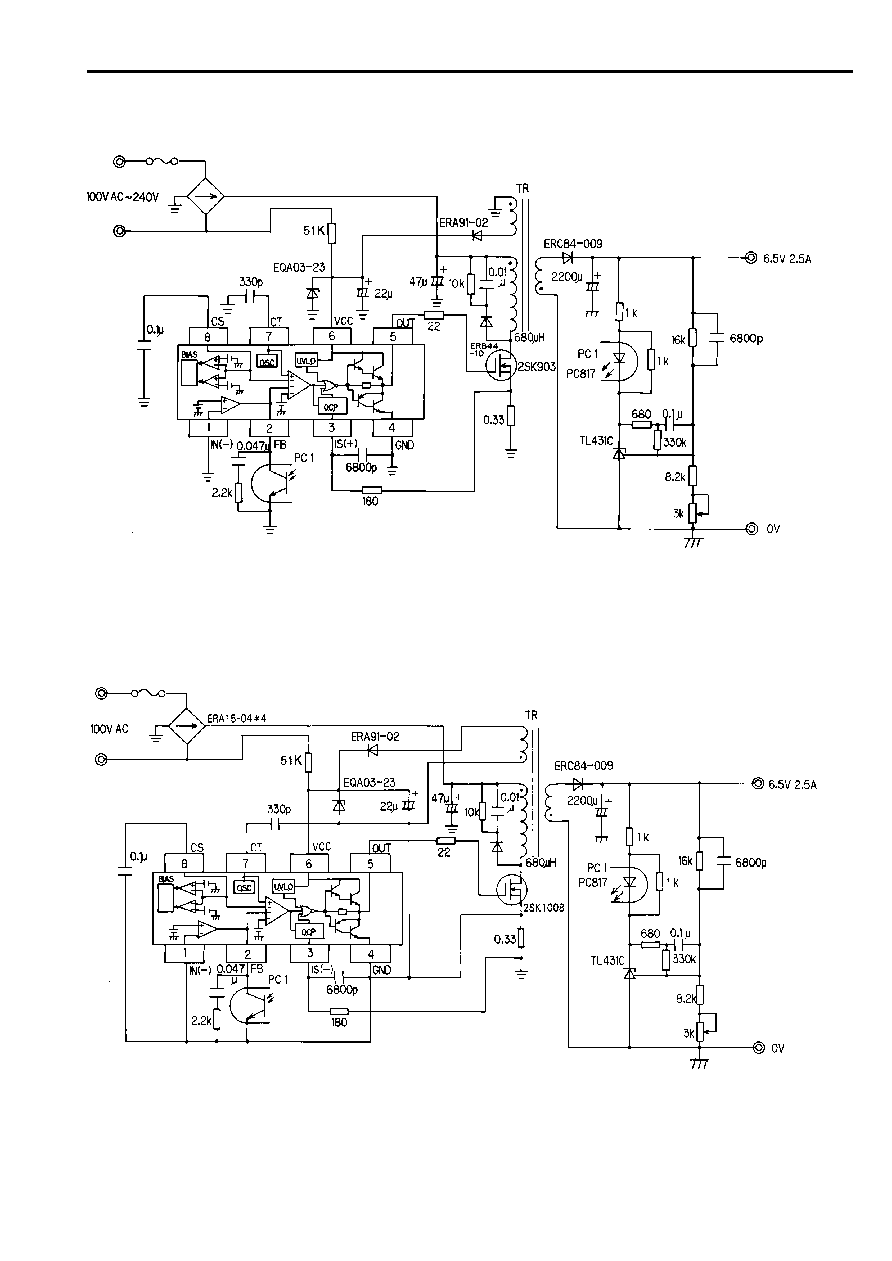
FA5304AP(S)/FA5305AP(S)
17
Example of FA5304AP(S) application circuit (3)
Example of FA5305AP(S) application circuit
Parts tolerances characteristics are not defined in the circuit design
sample shown above. When designing an actual circuit for a product,
you must determine parts tolerances and characteristics for safe and
economical operation.