 | –≠–ª–µ–∫—Ç—Ä–æ–Ω–Ω—ã–π –∫–æ–º–ø–æ–Ω–µ–Ω—Ç: FA5311BPS | –°–∫–∞—á–∞—Ç—å:  PDF PDF  ZIP ZIP |
FA531X series
1
FA5310BP(S), FA5314P(S), FA5316P(S)
FA5311BP(S), FA5315P(S), FA5317P(S)
s
Description
The FA531X series are bipolar ICs for switching power supply
control that can drive a power MOSFET.
These ICs contain many functions in a small 8-pin package.
With these ICs, a high-performance and compact power
supply can be created because not many external discrete
components are needed.
s
Features
∑ Drive circuit for connecting a power MOSFET
∑ Wide operating frequency range (5 to 600kHz)
∑ Pulse-by-pulse overcurrent limiting function
∑ Overload cutoff function (Latch or non-protection mode
selectable)
∑ Output ON/OFF control function by external signal
∑ Overvoltage cutoff function in latch mode
∑ Undervoltage malfunction prevention function
∑ Low standby current (90
µ
A typical)
∑ Exclusive choices by circuits (See selection guide on page 25)
∑ 8-pin package (DIP/SOP)
s
Applications
∑ Switching power supply for general equipment
Bipolar IC
For Switching Power Supply Control
s
Dimensions, mm
SOP-8
6.05
5.3
8.2
±
0.3
0.4
±
0.1
1.27
±
0.2
0.6
0.20
+0.1
≠0.05
0~10
∞
1
4
8
5
2.0max
DIP-8
FA531X series
s
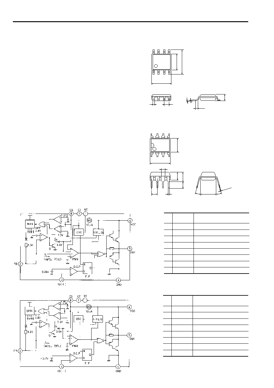
Block diagram
FA5310BP(S)/FA5311BP(S)/FA5316P(S)/FA5317P(S)
FA5314P(S)/FA5315P(S)
1
8
5
4
9.3
6.5
7.6
3.4
4.5max
1.5
3.0min
0~15∞
0~15∞
0.5
±
0.1
2.54
±
0.25
0.3
+0.1
≠0.05
Pin
Pin
Description
No.
symbol
1
RT
Oscillator timing resistor
2
FB
Feedback
3
IS (+)
Overcurrent (+) detection
4
GND
Ground
5
OUT
Output
6
VCC
Power supply
7
CT
Oscillator timing capacitor
8
CS
Soft-start and ON/OFF control
Pin
Pin
Description
No.
symbol
1
RT
Oscillator timing resistor
2
FB
Feedback
3
IS (≠)
Overcurrent (≠) detection
4
GND
Ground
5
OUT
Output
6
VCC
Power supply
7
CT
Oscillator timing capacitor
8
CS
Soft-start and ON/OFF control
FA531X series
2
s
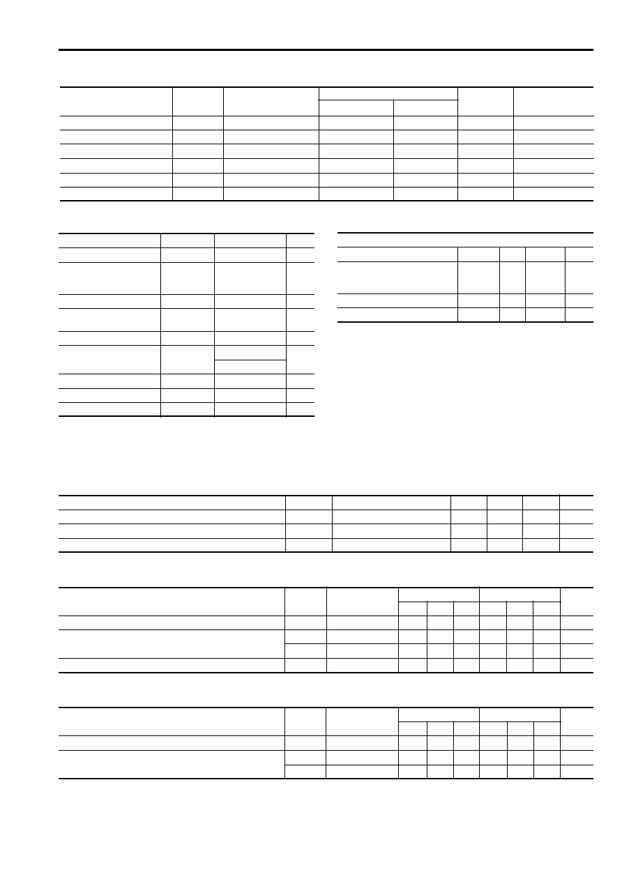
Selection guide
Type
FA5310BP(S)
46%
+
16.0V
8.70V
1.5A
Forward type
FA5311BP(S)
70%
+
16.0V
8.70V
1.5A
Flyback type
FA5314P(S)
46%
≠
15.5V
8.40V
1.5A
Forward type
FA5315P(S)
70%
≠
15.5V
8.40V
1.5A
Flyback type
FA5316P(S)
46%
+
15.5V
8.40V
1.0A
Forward type
FA5317P(S)
70%
+
15.5V
8.40V
1.0A
Flyback type
Max. duty
cycle (typ.)
Polarity of overcurrent
detection
Max. output
current
UVLO (typ.)
Application
ON threshold
OFF threshold
Notes:
*1
Derating factor Ta > 25
∞
C : 8.0mW/
∞
C (on PC board )
*2
Derating factor Ta > 25
∞
C : 5.5mW/
∞
C (on PC board )
s
Absolute maximum ratings
Item
Symbol
Rating
Unit
Supply voltage
V
CC
31
V
Output current
FA5310/11/14/15
I
O
±
1.5
A
FA5316/17
±
1.0
Feedback terminal input voltage
V
FB
4
V
Overcurrent detection
V
IS
≠0.3 to +4
V
terminal input voltage
CS terminal input current
I
CS
2
mA
Total power dissipation
P
d
800 (DIP-8) *
1
mW
(Ta=25
∞
C)
550 (SOP-8) *
2
Operating temperature
T
opr
≠30 to +85
∞
C
Junction temperature
T
j
125
∞
C
Storage temperature
T
stg
≠40 to +150
∞
C
s
Recommended operating conditions
Item
Symbol
Min.
Max.
Unit
Supply voltage
V
CC
10
30
V
Oscillator timing resistance
FA5310/11
R
T
3.3
10
k
FA5314/15/16/17
1
10
Soft-start capacitor
C
S
0.1
1
µ
F
Oscillation frequency
f
OSC
5
600
kHz
Soft-start circuit section
Item
Symbol
Test condition
FA5310/14/16
FA5311/15/17
Unit
Min.
Typ.
Max.
Min.
Typ.
Max.
Charge current (Pin 8)
I
CHG
Pin 8=0V
≠15
≠10
≠5
≠15
≠10
≠5
µ
A
Input threshold voltage (Pin 8)
V
TH CSO
Duty cycle =0%
0.90
0.90
V
V
TH CSM
Duty cycle =
D
MAX
1.90
2.30
V
s
Electrical characteristics (Ta=25
∞
C, Vcc=18V, f
OSC
=135kHz)
Oscillator section
Item
Symbol
Test condition
Min.
Typ.
Max.
Unit
Oscillation frequency
f
OSC
R
T
=5.1k
,
C
T
=360pF
125
135
145
kHz
Frequency variation 1 (due to supply voltage change)
f
dV
V
CC
=10 to 30V
±
1
%
Frequency variation 1 (due to temperature change)
f
dr
Ta=≠30 to +85
∞
C
±
1.5
%
Pulse width modulation circuit section
Item
Symbol
Test condition
FA5310/14/16
FA5311/15/17
Unit
Min.
Typ.
Max.
Min.
Typ.
Max.
Feedback terminal source current
I
FB
V
FB
=0
≠660
≠800
≠960
≠660
≠800
≠960
µ
A
Input threshold voltage (Pin 2)
V
TH FBO
Duty cycle =0%
0.75
0.75
V
V
TH FBM
Duty cycle =
D
MAX
1.80
2.30
V
Maximum duty cycle
D
MAX
43
46
49
66
70
74
%

FA531X series
3
Overcurrent limiting circuit section
Item
Symbol
Test condition
FA5310/11/16/17
FA5314/15
Unit
Min.
Typ.
Max.
Min.
Typ.
Max.
Input threshold voltage (Pin 3)
V
TH IS
0.21
0.24
0.27
≠0.21 ≠0.17 ≠0.14 V
Overcurrent detection terminal source current
I
IS
Pin 3=0V
≠300
≠200
≠100
≠240
≠160
≠80
µ
A
Delay time
T
PD IS
150
200
ns
Latch-mode cutoff circuit section
Item
Symbol
Test condition
Min.
Typ.
Max.
Unit
CS terminal sink current
I
SINK CS
Pin 8=6V, Pin 2=1V
25
45
65
µ
A
Cutoff threshold voltage (Pin 8)
V
TH CS
6.5
7.0
7.5
V
Overload cutoff circuit section
Item
Symbol
Test condition
Min.
Typ.
Max.
Unit
Cutoff-start voltage (Pin 2)
V
TH FB
2.6
2.8
3.1
V
Undervoltage lockout circuit section
Item
Symbol
Test condition
FA5310/11
FA5314/15/16/17
Unit
Min.
Typ.
Max.
Min.
Typ.
Max.
OFF-to-ON threshold voltage
V
CC ON
15.5
16.0
16.5
14.8
15.5
16.2
V
ON-to-OFF threshold voltage
V
CC OFF
8.20
8.70
9.20
7.70
8.40
9.10
V
Overall device
Item
Symbol
Test condition
Min.
Typ.
Max.
Unit
Standby current
I
CC ST
V
CC
=14V
90
150
µ
A
Operating-state supply current
I
CC OP
9
15
mA
OFF-state supply current
I
CC OFF
1.1
1.8
mA
Cutoff-state supply current
I
CCL
1.1
1.8
mA
Output section
Item
Symbol
Test condition
Min.
Typ.
Max.
Unit
FA5310/11/14/15
FA5316/17
L-level output Voltage
V
OL
I
O
=100mA
I
O
=50mA
1.30
1.80
V
H-level output Voltage
V
OH
I
O
=≠100mA
I
O
=≠50mA
16.0
16.5
V
V
CC
=18V
V
CC
=18V
Rise time
tr
No load
No load
50
ns
Fall time
tf
No load
No load
50
ns
Output ON/OFF circuit section
Item
Symbol
Test condition
Min.
Typ.
Max.
Unit
CS terminal source current
I
source cs
Pin 8=0V
≠15
≠10
≠5
µ
A
OFF-to-ON threshold Voltage (Pin 8)
V
TH ON
CS terminal voltage OFF
ON
0.56
V
ON-to-OFF threshold Voltage (Pin 8)
V
TH OFF
CS terminal voltage ON
OFF
0.42
V
4
FA531X series
s
Description of each circuit
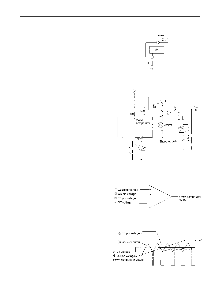
1. Oscillator (See block diagram)
The oscillator generates a triangular waveform by charging and
discharging a capacitor. CT pin voltage oscillates
between an upper limit of approx. 3.0V and a lower limit of
approx. 1.0V. The oscillation frequency is determined by a
external resistance and capacitance shown in figure 1, and
approximately given by the following equation:
The recommended oscillation range is between 5k and
600kHz.
The oscillator output is connected to a PWM comparator.
2. Feedback pin circuit
Figure 2 gives an example of connection in which an
optocoupler is used to couple the feedback signal to the FB pin.
It is designed to be strong against noise and will not create
parasitic oscillation so much, because the output impedance at
the FB pin is as low as 4k to 5k. If this circuit causes power
supply instability, the frequency gain can be decreased by
connecting R
4
and C
4
as shown in figure 2. R
4
should be
between several tens of ohms to several kiloohms and C
4
should be between several thousand picofarads to one
microfarads.
3. PWM comparator
The PWM comparator has four inputs as shown in Figure 3.
Oscillator output
x
is compared with CS pin voltage
, FB pin
voltage
, and DT voltage
{
. The lowest of three inputs
,
,
and
{
is compared with output
x
. If it is lower than the
oscillator output, the PWM comparator output is high, and if it is
higher than the oscillator output, the PWM comparator
output is low (see Fig. 4).
The IC output voltage is high during when the comparator
output is low, and the IC output voltage is low during when the
comparator output is high.
When the IC is powered up, CS pin voltage
controls soft start
operation. The output pulse then begins to widen gradually.
During normal operation, the output pulse width is determined
within the maximum duty cycle set by DT voltage
{
under the
condition set by feedback signal
, to stabilize the output
voltage.
f (kH
Z
) =
10
6
.........(1)
Fig. 1 Oscillator
Fig. 2 Configuration with optocoupler (FB pin input)
Fig. 3 PWM comparator
Fig. 4 PWM comparator timing chart
4R
T
(k
) ∑ C
T
(pF)
5
FA531X series
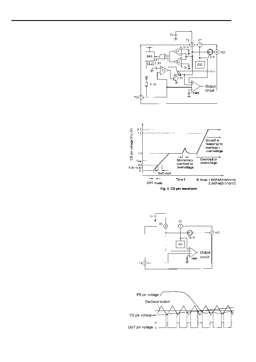
4. CS pin circuit
As shown in Figure 5 capacitor C
S
is connected to the CS pin.
When power is turned on, the constant current source (10
µ
A)
begins to charge capacitor C
S
. Accordingly, the CS pin
voltage rises as shown in Figure 6. The CS pin is connected to
an input of the PWM comparator. The device is in soft-start
mode while the CS pin voltage is between 0.9V and 1.9V
(FA5310/14/16) and between 0.9V and 2.3V(FA5311/15/17).
During normal operation, the CS pin is clamped at 3.6V by
internal zener diode Zn. If the output voltage drops due to an
overload, etc., the clamp voltage shifts from 3.6V to 8.0V. As a
result, the CS pin voltage rises to 8.0V. The CS pin is also
connected to latch comparator C2. If the pin voltage rises
above 7.0V, the output of comparator C2 goes high to turn off
the bias circuit, thereby shutting the output down. Comparator
C2 can be used not only for shutdown in response to an
overload, but also for shutdown in response to an overvoltage.
Comparator C1 is also connected to the CS pin, and the bias
circuit is turned off and the output is shut down if the CS pin
voltage drops below 0.42V. In this way, comparator C1 can
also be used for output on/off control.
As explained above, the CS pin can be used for soft-start
operation, overload and overvoltage output shutdown and
output on/off control.
Further details on the four functions of the CS pin are given
below.
4.1 Soft start function
Figure 7 shows the soft start circuit. Figure 8 is the soft-start
operation timing chart. The CS pin is connected to capacitor
C
S
. When power is turned on, a 10
µ
A constant-current source
begins to charge the capacitor. As shown in the timing chart,
the CS pin voltage rises slowly in response to the charging
current. The CS pin is connected internally to the PWM
comparator. The comparator output pulse slowly widens as
shown in the timing chart.
The soft start period can be approximately evaluated by the
period ts from the time the IC is activated to the time the output
pulse width widens to 30%. Period ts is given by the following
equation:
t
S
(m
S
)=160C
S
(
µ
F)...................................(2)
Fig. 5 CS pin circuit
Fig. 6 CS pin waveform
Fig. 7 Soft-start circuit
Fig. 8 Soft-start timing chart