 | –≠–ª–µ–∫—Ç—Ä–æ–Ω–Ω—ã–π –∫–æ–º–ø–æ–Ω–µ–Ω—Ç: FA5331PM | –°–∫–∞—á–∞—Ç—å:  PDF PDF  ZIP ZIP |

FA5331P(M)/FA5332P(M)
1
s
Description
FA5331P(M) and FA5332P(M) are control ICs for a power
factor correction system. These ICs use the average current
control system to ensure stable operation. With this system, a
power factor of 99% or better can be achieved.
FA5331P(M) is a 1st generation IC and FA5332P(M) is 2nd
generation IC which light-load characteristics are improved.
s
Features
∑ Drive circuit for connecting a power MOS-FET(Io =
±
1.5A)
∑ Pulse-by-pulse overcurrent and overvoltage limiting function
∑ Output ON/OFF control function by external signals
∑ External synchronizing signal terminal for synchronous
operation with other circuits
∑ Undervoltage malfunction prevention function
∑ Low standby current (90
µ
A typical) for simple start-up circuit
∑ 16-pin package (DIP/SOP)
∑
±
2% accuracy reference voltage for setting DC output and
overvoltage protection [FA5332P(M) only]
∑ When there is a possibility of light-load operation,
FA5332P(M) is suitable.
s
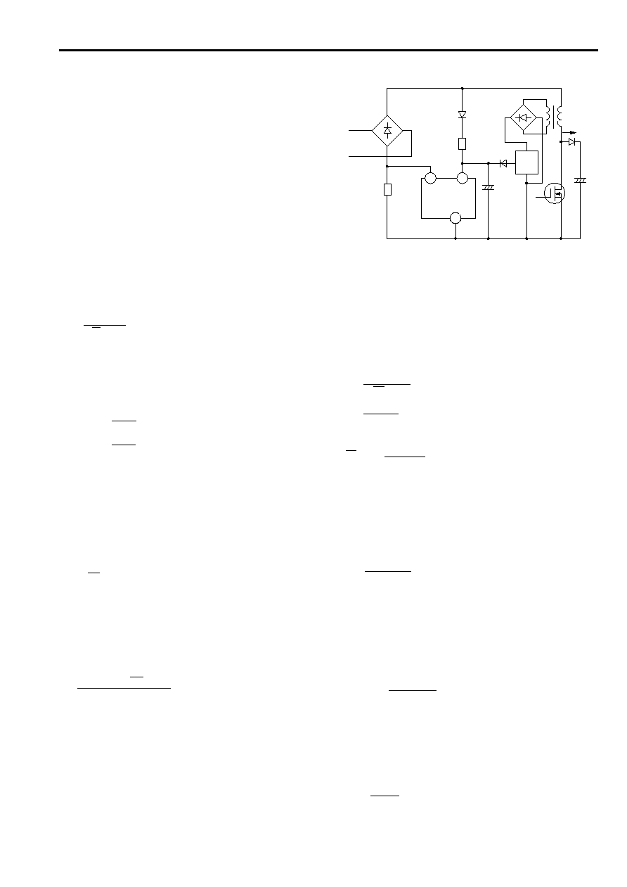
Block diagram
FA5331P(M)/FA5332P(M)
s
Dimensions, mm
SOP-16
1
10.06
8
9
16
5.5
0.7
2.0
0~10∞
1.27
±
0.2
7.8
±
0.3
0.40
±
0.1
0.20
+0.1
≠0.05
DIP-16
FA5331P
1
16
9
8
19.4
6.5
7.6
3.4
4.3max
1.5
0.81
3.1min
0.2min
0~15∞
0~15∞
0.5
±
0.1
2.54
±
0.25
0.3
+0.1
≠0.05
Bipolar IC
For Power Factor Correction
FA5332P
1
16
9
8
19.2
6.3
7.62
3.6
5.06max
1.3
0.71
2.54min
0.51min
0~15∞
0~15∞
0.48
±
0.1
2.54
±
0.25
0.25
+0.1
≠0.05
Pin
Pin
Description
No.
symbol
1
IFB
Current error amplifier output
2
IIN≠
Inverting input to current error amplifier
3
VDET
Multiplier input
4
OVP
Overvoltage protection input
5
VFB
Voltage error amplifier output
6
VIN≠
Inverting input to voltage error amplifier
7
GND
Ground
8
OUT
Output
9
VC
Power supply to output circuit
10
VCC
Power supply
11
CS
Soft-start
12
ON/OFF
Output ON/OFF control input
13
REF
Reference voltage
14
SYNC
Oscillator synchronization input
15
CT
Oscillator timing capacitor and resistor
16
IDET
Non-inverting input to current error amplifier

2
FA5331P(M)/FA5332P(M)
Notes:
*
1
Derating factor Ta > 25
∞
C: 6.8mW/
∞
C (on PC board)
*
2
Derating factor Ta > 25
∞
C: 5.2mW/
∞
C (on PC board)
Voltage error amplifier section
Item
Symbol
Test condition
FA5331P(M)
FA5332P(M)
Unit
Min.
Typ.
Max.
Min.
Typ.
Max.
Reference voltage
V
r
1.48
1.54
1.60
1.519 1.550 1.581 V
Input bias current
I
BE
≠500
≠50
≠500
≠50
nA
Open-loop voltage gain
A
VE
80
80
dB
Output voltage
V
OE+
No load
3.5
3.8
3.5
3.8
V
V
OE≠
50
200
50
200
mV
Output source current
I
OE+
V
OE
=0V
≠900
≠900
µ
A
s
Electrical characteristics (Ta=25
∞
C, C
T
=470pF, R
T
=22k
, V
CC
=V
C
=18V)
Oscillator section
Item
Symbol
Test condition
FA5331P(M)
FA5332P(M)
Unit
Min.
Typ.
Max.
Min.
Typ.
Max.
Oscillation frequency
f
OSC
C
T
=470pF
68
75
82
68
75
82
kHz
R
T
=22k
Frequency variation 1 (due to supply voltage change)
f
dV
V
CC
=10 to 30V
1
1
3
%
Frequency variation 1 (due to temperature change)
f
dT
Ta=≠30 to +85
∞
C
5
5
8
%
Output peak voltage
V
OSC
3.55
3.55
V
Synchronizing input peak voltage
V
SYNC
SYNC terminal voltage 1.5
1.5
V
s
Absolute maximum ratings
Item
Symbol
Rating
Unit
FA5331P(M)
FA5332P(M)
Supply voltage
V
CC
,
V
C
30
30
V
Output current
I
O
±
1.5
±
1.5
A
Input voltage
V
SYNC
,
V
ON/OFF
,
V
VIN≠
≠0.3 to +5.3
≠0.3 to +5.3
V
V
VDET
,
V
OVP
V
IDET
≠10.0 to +5.3
≠10.0 to +5.3
V
Total power dissipation
P
d
850 (DIP-16) *
1
850 (DIP-16) *
1
mW
(Ta=25
∞
C)
650 (SOP-16) *
2
650 (SOP-16) *
2
Operating temperature
T
opr
≠30 to +85
≠30 to +85
∞
C
Storage temperature
T
stg
≠40 to +150
≠40 to +150
∞
C
s
Recommended operating conditions
Item
Symbol
FA5331P(M)
FA5332P(M)
Unit
Min.
Max.
Min.
Max.
Supply voltage
V
CC
,
V
C
10
28
10
28
V
IDET terminal input voltage
V
IDET
≠1.0
0
≠1.0
0
V
VDET terminal input voltage
V
VDET
0
2.0
0
2.4
V
VDET terminal peak input voltage
V
PVDET
0.65
2.0
0.65
2.4
V
Oscillator timing capacitance
C
T
≠
≠
330
1000
pF
Oscillator timing resistance
R
T
≠
≠
10
75
k
Oscillation frequency
f
OSC
10
220
15
150
kHz
Noise filter resistance connected to IDET terminal
R
n
0
100
0
27
FA5331P(M)/FA5332P(M)
3
Current error amplifier section
Item
Symbol
Test condition
FA5331P(M)
FA5332P(M)
Unit
Min.
Typ.
Max.
Min.
Typ.
Max.
Input threshold voltage
V
TH IDET
V
DET
=0V
≠
≠
≠
0
30
60
mV
V
FB
=
V
r
,
R
n
=30
Input bias current
I
BC
I
DET
=0V
≠350
≠230
≠350
≠250
≠150
µ
A
Open-loop voltage gain
A
VC
80
80
dB
Output voltage
V
OC+
No load
3.5
3.8
3.5
3.8
V
V
OC≠
50
200
50
200
mV
Output source curent
I
OC+
V
IFB
=0V
≠900
≠900
µ
A
Reference voltage section
Item
Symbol
Test condition
FA5331P(M)
FA5332P(M)
Unit
Min.
Typ.
Max.
Min.
Typ.
Max.
Output voltage
V
REF
4.8
5.0
5.2
4.8
5.0
5.2
V
Voltage variation 1 (by supply voltage variation)
V
RDV
V
CC
=10 to 30V
25
25
mV
Voltage variation 2 (by load change)
V
RDT
I
OR
=0.1 to 2mA
2
2
5
mV
Multiplier section
Item
Symbol
Test condition
FA5331P(M)
FA5332P(M)
Unit
Min.
Typ.
Max.
Min.
Typ.
Max.
VDET terminal input voltage
V
MVDET
0
2.0
0
2.4
V
VFB terminal input voltage
V
MVFB
1.5
3.5
1.5
3.5
V
Output current
I
M
V
IIN≠
=0V
≠65
≠65
µ
A
Output voltage coefficient
K
≠1.0
≠1.0
≠
Pulse width modulation circuit section
Item
Symbol
Test condition
FA5331P(M)
FA5332P(M)
Unit
Min.
Typ.
Max.
Min.
Typ.
Max.
Maximum duty cycle
D
MAX
89
92
95
89
92
95
%
Soft-start circuit section
Item
Symbol
Test condition
FA5331P(M)
FA5332P(M)
Unit
Min.
Typ.
Max.
Min.
Typ.
Max.
Input threshold voltage
V
THCSO
Duty cycle=0%
0.1
0.1
V
V
THCSM
Duty cycle=D
MAX
3.55
3.55
V
Charge current
I
CHG
CS terminal=0V
≠10
≠10
µ
A
Output circuit section
Item
Symbol
Test condition
FA5331P(M)
FA5332P(M)
Unit
Min.
Typ.
Max.
Min.
Typ.
Max.
Output voltage
V
OL
I
O
=100mA
1.3
1.8
1.3
1.8
V
V
OH
I
O
=≠100mA
15.5
16.5
15.5
16.5
V
V
CC
=18V
Rise time
t
r
No load
300
300
ns
Fall time
t
r
No load
200
200
ns
4
FA5331P(M)/FA5332P(M)
Overvoltage protection circuit section
Item
Symbol
Test condition
FA5331P(M)
FA5332P(M)
Unit
Min.
Typ.
Max.
Min.
Typ.
Max.
Input threshold voltage
V
THOVP
OVP terminal
1.56
1.64
1.72
1.617 1.650 1.683 V
voltage
Input threshold voltage/reference voltage(V
THOVP
/ Vr)
≠
≠
≠
1.044 1.065 1.086 ≠
Delay time
T
PDOVP
200
200
ns
Output ON/OFF circuit section
Item
Symbol
Test condition
FA5331P(M)
FA5332P(M)
Unit
Min.
Typ.
Max.
Min.
Typ.
Max.
Threshold voltage
V
THONOFF
Ta=≠30
∞
C
≠
≠
≠
3.7
4.3
V
Ta=+25
∞
C
2.0
3.5
2.8
3.4
V
Ta=+85
∞
C
≠
≠
≠
1.5
2.8
V
Input current at ON
I
THON
ON/OFF terminal
60
120
≠
≠
µ
A
voltage=3.5V
ON/OFF terminal
≠
≠
10
40
µ
A
voltage=
V
THONOFF
Undervoltage lockout circuit section
Item
Symbol
Test condition
FA5331P(M)
FA5332P(M)
Unit
Min.
Typ.
Max.
Min.
Typ.
Max.
OFF to ON threshold voltage
V
THUON
14.3
15.3
16.3
14.6
15.3
16.0
V
ON to OFF threshold voltage
I
THUOFF
7.6
8.3
9.0
7.6
8.3
9.0
V
Voltage hysteresis
V
UHYS
7.0
7.0
V
Overall device
Item
Symbol
Test condition
FA5331P(M)
FA5332P(M)
Unit
Min.
Typ.
Max.
Min.
Typ.
Max.
Standby current
I
CCST
V
CC
=14V
90
140
90
140
µ
A
Operating-state supply current
I
CCOP
10
15
10
15
mA
OFF-state supply current
I
CCOFF
Pin 12=0V
1.1
1.8
1.1
1.8
mA
Overcurrent limiting circuit section
Item
Symbol
Test condition
FA5331P(M)
FA5332P(M)
Unit
Min.
Typ.
Max.
Min.
Typ.
Max.
Input threshold voltage
V
THOCP
IDET terminal
≠1.25 ≠1.15 ≠1.05 ≠1.20 ≠1.10 ≠1.00 V
voltage
Delay time
T
PDOCP
200
200
ns
5
FA5331P(M)/FA5332P(M)
s
Description of each circuit
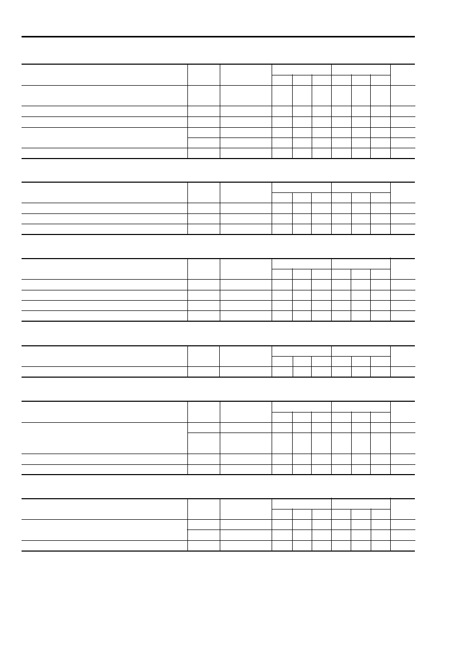
1. Oscillator section
This section outputs sawtooth waves oscillating between 0.15
and 3.55V using the capacitor charge and discharge
characteristics. Figure 1 shows how to connect the required
external components to this circuit. The oscillation frequency
is determined by the C
T
and R
T
values. The relationship
between the C
T
and R
T
values is shown in characteristic
curves. Pin 14 (SYNC) is a synchronizing input terminal
whose threshold voltage is about 1V. As Fig. 1 shows, input
rectangular synchronizing signal waves to pin 14 through an
RC circuit. Set the free-running frequency about 10% lower
than the synchronizing signal frequency. Connect a clamp
diode (D1) to prevent an unwanted current inside the IC.
2. Voltage error amplifier and overvoltage limiting circuit
The voltage error amplifier forms a voltage feedback loop to
keep the output voltage stable. The positive input terminal of
this amplifier is connected to the reference voltage (Vr). Fig. 2
shows how to connect the required external components to
this circuit.
The output voltage (Vo) is as follows:
............................................................................... (1)
FA5331: Vr=1.54V(typ.)
FA5332: Vr=1.55V(typ.)
Connect a resistor and a capacitor in parallel across error
amplifier output pin 5 and error amplifier negative input pin
6 to set the voltage gain (Av).
The Av value is as follows:
Av =
R4
R3 ( 1 + j
C1 ∑ R4 )
............................... (2)
Error amplifier cutoff frequency (fc) is as follows:
fc =
1
2
C1 ∑ R4
................................................. (3)
If 100 or 120Hz ripples appear at the error amplifier output, the
active filter does not operate stably. To ensure stable
operation, set the fc value to about 1Hz.
An overvoltage detection comparator (C1) is built in to limit the
voltage if the output voltage exceeds the design value. The
reference input voltage (Vp) is as follows:
Vp =
∑ Vr ............................................................. (4)
=1.065
The connections shown in Fig. 2 limit the output voltage to
times the design value.
15
R
OSC
CT
RT
CT
D1
Csy
SYNC
13 REF
14
Fig. 1 Oscillator
6
R2
R1
Vo
MUL
5
R3
C1
Vr
R4
_
+
A1
F.F
Vp
4
C1
ER.AMP
OVP
Fig. 2 Voltage error amplifier and overvoltage limiting circuit
Vo =
R1 + R2
R1
∑ Vr
6
FA5331P(M)/FA5332P(M)
3. Current error amplifier and overcurrent limiting circuit
The current error amplifier forms a current loop to change the
input circuit current into sinusoidal waves. As Fig. 3 shows, the
multiplier output is connected to pin 2 (IIN ≠) through a resistor
(RA) to input the reference current signal. Pin 16 (IDET) is a
current input terminal. Design the circuit so that the voltage at
pin 16 will be within the range from 0 (GND potential) to ≠1.0V.
Connect a phase correction resistor and capacitors across pin
1 (amplifier output) and pin 2. See Fig. 4 for the expected gain
characteristics of the circuit shown in Fig. 3.
Here,
Z =
1
2
R5 ∑ C3
.................................................. (5)
p =
1
2
R5 ∑ C
............................................. (6)
C =
C2 ∑ C3
C2 + C3
The voltage gain (G1) between Z and P of the circuit (gain
between pins 16 and 1) is given as follows:
G1 = 20 ∑ log
10
{ 0.75 ( R5
RA
+ 1) }
.................... (7)
Ensure an adequate phase margin by selecting C1 and C2 so
that the p/z ratio is about 10. The current error amplifier output
is used as an input to the comparator for PWM.
The overcurrent detection comparator (C2) limits an
overcurrent. The threshold voltage for overcurrent detection at
pin 16 is ≠1.15V for FA5331 and ≠1.10V for FA5332. Connect
noise filters Rn and Cn to prevent the voltage at pin 16 from
fluctuating due to noise, causing the comparator to malfunction.
For Rn, select a resistor of up to 100
for FA5331 and up to
27
for FA5332. (See P64, 4. No-load operation )
4. Comparator for PWM
Figure 5 shows the comparator for PWM. When the oscillator
output (Va) is smaller than the current error amplifier output
(Vc), the comparator output is high and the output ON signal is
generated at pin 8. Pin 11 (CS) is a terminal for soft start. This
terminal charges capacitor C4 with the internal constant current
(10
µ
A) for a soft start. Priority is given to Vb and Vc whichever
is lower.
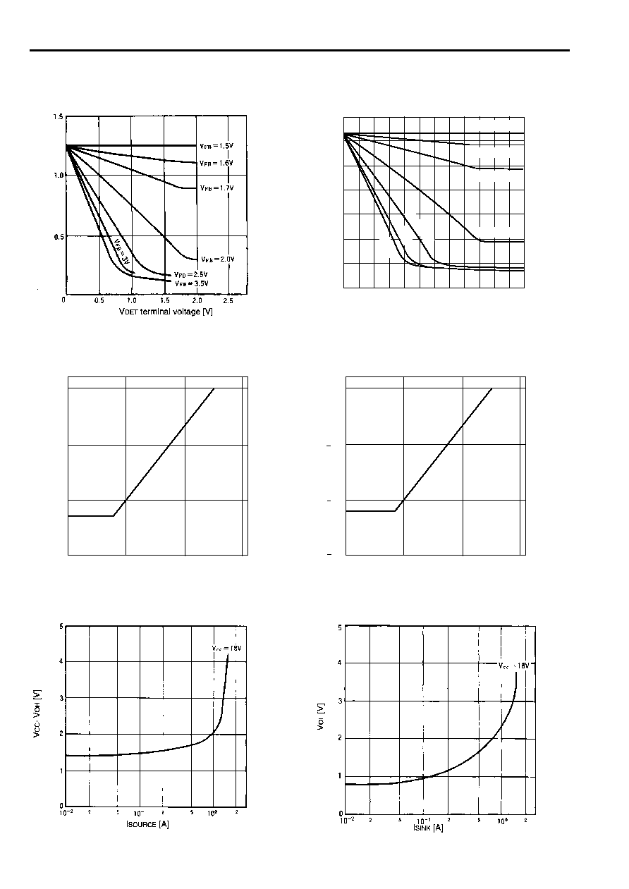
5. Multiplier
The multiplier generates a reference current signal. Input a
fully rectified sinusoidal signal voltage into pin 3 (VDET).
Design the circuit to keep the peak voltage at pin 3 within a
range from 0.65V to 2V for FA5331 and 0.65V to 2.4V for
FA5332. The multiplier output voltage (Vm) is roughly given as
follows (see Fig. 6):
Vm = 1.25 ≠ (Ve ≠1.55) ∑ Vs .................................... (8)
As Fig. 3 shows Vm is internally connected to pin 2 (IIN≠) of the
current error amplifier A2 through a 10k
resistor. (See the
characteristic curve, page 66 for the input and output
characteristics of the multiplier.)
Fig. 6 Multiplier
Fig. 4 Voltage gain-frequency
Fig. 3 Current error amplifier and overcurrent limiting circuit
Fig. 5 PWM comparator
PWM
VREF
_
+
A2
F.F
Vocp
2
1
4
16
Rn
Cn
RC
5k
RB
15k
5V
C2
C3
C2
Vm
RA
10k
R5
comparator
Current
detection
MUL
CURR.AMP
OPC
G1
(dB)
Voltage gain
Z
P
Frequency
R7
Ve
ER.AMP(A1) output
Vs
Vm
V
IN
R6
3
MUL
C4
Vb
10
µ
A
CS
C3
Oscillator output Va
PWM comparator
CURR.AMP(A2) output Vc
11

7
FA5331P(M)/FA5332P(M)
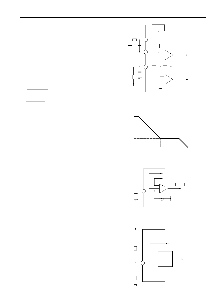
6. ON/OFF control input circuit
Figure 7 shows the ON/OFF control input circuit. If pin 12 is set
to the high level (enable), this IC outputs pulses from the OUT
pin. If pin 12 is set to the low level (disable), the internal bias
power (reference voltage) goes off and the IC current
consumption becomes about 1/10 that of its ON state. The
output level of pin 11 (CS for soft start) also goes low.
7. Output circuit
As Fig. 8 shows, pin 9 is configured as the high power terminal
(VC), independent of the IC power terminal (VCC). This pin
allows an independent drive resistance when the power
MOSFET is ON and OFF. If the drive resistances in the ON and
OFF states are Rg (on) and Rg (off), the following formulas can
be used to determine the total gate resistance
Rg:
Rg (on) = Rg1 + Rg2 ............................................. (9)
Rg (off) = Rg2 ..................................................... (10)
In the standby state, the output level of pin 8 is held low.
If the potential at the drain terminal of the power MOSFET
fluctuates, the gate-drain capacitance may drive the IC output
voltage at pin 8 to below 0. Once the voltage at pin 8 reaches
≠0.6V, an unwanted current flows in the IC and a large abnormal
current flows in the output circuit when the output transistor is
turned on. To prevent this, connect a Schottky diode across the
gate and source of the power MOSFET.
Fig. 7 ON/OFF control input circuit
Fig. 8 Output circuit
1k
100k
Vcc
12
ON/OFF
10
µ
A
Rg2
Rg1
GND
VCC
Cv
+
10
9
8
7
Pin7
Schottky
diode
8
FA5331P(M)/FA5332P(M)
s
Design advice
1. Start circuit
Figure 9 shows a sample start circuit. Since the IC current
while the Vcc pin voltage rises from 0V to V
THON
is as small as
90
µ
A (typ.), the power loss in resistor R
A
is small. If an
additional winding is prepared in the voltage step-up inductor
(L), power to the control circuit can be supplied from this
circuit. However, the voltage must be stabilized by a regulator
circuit (REG) to prevent an excess rise of the IC supply voltage
(Vcc). Use fast or ultra-fast rectifier diodes for the rectifier circuit
(DB1) of the winding for high-frequency operation.
2. Current sensing resistor
The current sensing resistor (Rs) detects the current in the
inductor. Rs is used to make the input current sinusoidal. The
current in the inductor produces a negative voltage across Rs.
The voltage is input to IC pin 16 (IDET). Determine the value
of Rs so that the peak voltage of the IDET pin is ≠1V.
Rs =
Vin
2 ∑ Pin
.................................................. (11)
Vin: Minimum AC input voltage (effective value) [V]
Pin: Maximum input power [W]
Since the threshold voltage of the overcurrent limiting circuit
(pin 16) is ≠1.15V for FA5311 for and ≠1.10V for FA5332, the
peak input current limit (ip) is determined by:
............................................................................. (12)
3. Voltage step-up type converter
Figure 9 shows the basic circuit of a voltage step-up type
converter which is used as a power factor correction.
(a) Output voltage
For stable operation, set the output voltage to be 10V or more
over the peak value of the maximum input voltage. When
using this IC for an active filter, set the output voltage (Vo) as
follows:
Vo
2 ∑ Vin + 10V ............................................ (13)
Vin: Maximum AC input voltage [V]
(effective value of sinusoidal wave)
(b) Voltage step-up inductor
When using a voltage step-up converter in continuous current
mode, the ratio of inductor current ripple to the input peak
current is set to about 20%. Determine the inductance as
follows:
L
Vin
2
( Vo ≠
2 ∑ Vin )
∑ fs ∑ Pin ∑ Vo
................................ (14)
Vin: Minimum AC input voltage (effective value) [V]
:
Ratio of inductor current ripple (peak to peak value) to the
input peak current (about 0.2)
fs:
Switching frequency [Hz]
Pin: Converter's maximum input power [W]
As the characteristic curves on page 66 show, the peak
voltage at pin 3 should be at least 0.65V, even when the AC
input voltage is minimal. Considering this, determine R6 and
R7 shown in Fig. 6.
Fig. 9 Start circuit
Example: FA5332
When Vin is 85V and Pin is 300W, the formulas of (11)
and (12) can be calculated as:
Rs =
85
2 ∑ 300
= 0.2 [
]
ip =
1.10
0.2
= 5.5 [ A ]
2 ∑ 85 ∑
R6
R6 + R7
= 0.65 [ V ]
And,
If R6 is set to 2.7k
to satisfy these formulas, R7 becomes
480k
.
Example:
When Vin is 85V, Vo is 385V, and
is 0.2, the formula of (14)
can be calculated as:
L
2.48
!
10
4
fs ∑ Pin
[ H ] ......................................... (15)
(c) Smoothing capacitor
When a voltage step-up converter is used in a power factor
correction circuit, the input current waveform is regulated to be
in-phase with the input voltage waveform. Therefore, ripple
noise of twice the input line frequency appears at the output.
The output voltage (
o
) is represented as:
o
= Vo ≠
Io
2 ∑
o
∑C
∑ Sin 2
o
t
................... (16)
Vo: Average output voltage
Io: Output current
o
: 2
fo (fo: Input power frequency, 50 or 60Hz)
C: Smoothing capacitor value
Therefore, the peak-to-peak value of the output ripple voltage
Vrp is given by:
Vrp =
Io
o
C
..................................................... (17)
Using formula (17), determine the necessary C value.
16
10
7
C
A
R
A
R
S
Vcc
AC input
DB1
L
REG
C
FA5331/FA5332
Io
1.15
Rs
FA5331: ip=
FA5332: ip= 1.10
Rs

FA5331P(M)/FA5332P(M)
9
4. No-load operation
The following condition should be meet to prevent from
overvoltage and audible noise during no-load or light-load
operation.
For FA5331 (Fig.10)
0.85∑
R
OFST
(k
)
where, =
and, R
n
100
and, R
X
: don't connect.
∑You must not connect R
X
which reduces DC gain of current
error amplifier.
∑You can connect R
5
which is series with capacitor C
3
.
For FA5332 (Fig.11)
R
n
27
and, R
X
: don't connect.
∑You must not connect R
X
which reduces DC gain of current
error amplifier.
∑You can connect R
5
which is series with capacitor C
3
.
∑If you connect R
OFST
, dead time of AC input current will
extend.
5. How to prevent from intermittent switching of low
frequency
An intermittent switching, which frequency is lower than 10Hz,
occurs in some applications.
In this case, it is possible to prevent from this intermittent
switching to reduce feedback gain by decreasing the
resistance of R4. (See Fig. 2)
You must check the effect thoroughly because this intermittent
switching depends on load, temperature and input condition.
Fig.10
Fig.11
(3.5∑10
3
≠0.26∑R
n
)∑12
42+0.26∑R
n
13 REF
IIN≠
IFB
C2
C3
R5
Rn
Cn
Current
detection
Rx
IDET
R
OFST
FA5331
2
1
16
Current
detection
13 REF
IIN≠
IFB
C2
C3
R5
Rn
Cn
Rx
IDET
R
OFST
FA5332
2
1
16

10
FA5331P(M)/FA5332P(M)
s
Characteristic curves (Ta = 25
∞
C)
Oscillation frequency (f
OSC
) vs.
timing resistor resistance (R
T
)
FA5331
FA5332
Oscillation frequency (f
OSC
) vs.
ambient temperature (Ta)
FA5331
FA5332
Output duty cycle vs. CS terminal voltage (V
CS
)
ON/OFF control terminal current vs.
ON/OFF control terminal voltage
R
T
[k
]
fosc [kHz]
10
20
50
100
200
10
50
20
100
C
T
=330pF
C
T
=470pF
C
T
=680pF
T
a
[∞C]
fosc [kHz]
68
70
69
71
73
74
75
76
77
78
72
≠40
60
0
≠20
20
40
80
100
Vcc=18V
C
T
=470pF
R
T
=22k
FA5331P(M)/FA5332P(M)
11
IIN≠ terminal voltage vs. VDET terminal voltage
Multiplier I/O
FA5331
FA5332
IDET terminal voltage vs. IIN≠ terminal voltage
Normal operation
FA5331
FA5332
H-level output voltage (V
OH
) vs.
L-level output voltage(V
OL
) vs.
output source current (I
SOURCE
)
output sink current (I
SINK
)
IDET
terminal voltage [V]
≠1.5
≠1.0
≠0.5
0
0
0.5
1.0
1.5
IIN≠ terminal voltage [V]
V
DET
terminal voltage [V]
0
0.4
0.2
0.6
1.0
1.2
1.4
0.8
0
2
0.8
0.4
1.2
1.6
2.4
VFB=1.5V
VFB=1.6V
VFB=1.7V
VFB=2.0V
VFB=2.5V
VFB=3.0V
VFB=3.5V
IIN≠ terminal voltage [V]
IDET
terminal voltage [V]
1.5
1.0
0.5
0
0
0.5
1.0
1.5
IIN≠ terminal voltage [V]
IIN≠ terminal voltage [V]
12
FA5331P(M)/FA5332P(M)
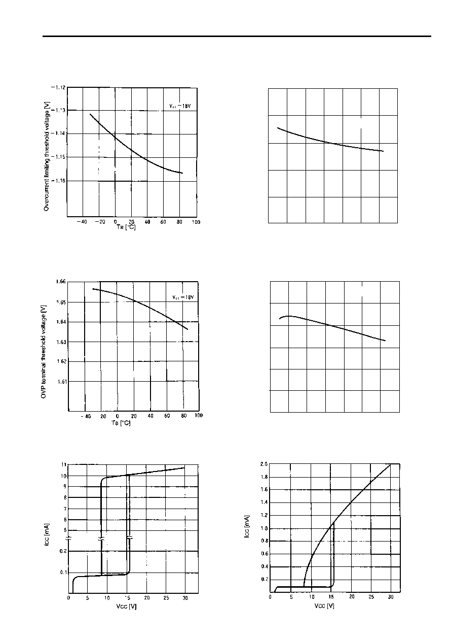
Overcurrent limiting threshold voltage vs.
ambient temperature (Ta)
FA5331
FA5332
OVP terminal threshold voltage vs.
ambient temperature (Ta)
FA5331
FA5332
Supply current (I
CC
) vs. supply voltage (V
CC
)
Supply current (I
CC
) vs. supply voltage (V
CC
)
Normal operation
OFF mode
≠1.13
≠1.12
≠1.11
≠1.1
≠1.09
≠1.08
≠40
60
0
≠20
20
40
80
100
Vcc=18V
Overcurrent limiting threshold voltage [V]
T
a
[∞C]
1.61
1.62
1.63
1.64
1.65
1.66
1.67
≠40
60
0
≠20
20
40
80
100
Vcc=18V
OVP
terminal threshold voltage [V]
T
a
[∞C]
FA5331P(M)/FA5332P(M)
13
s
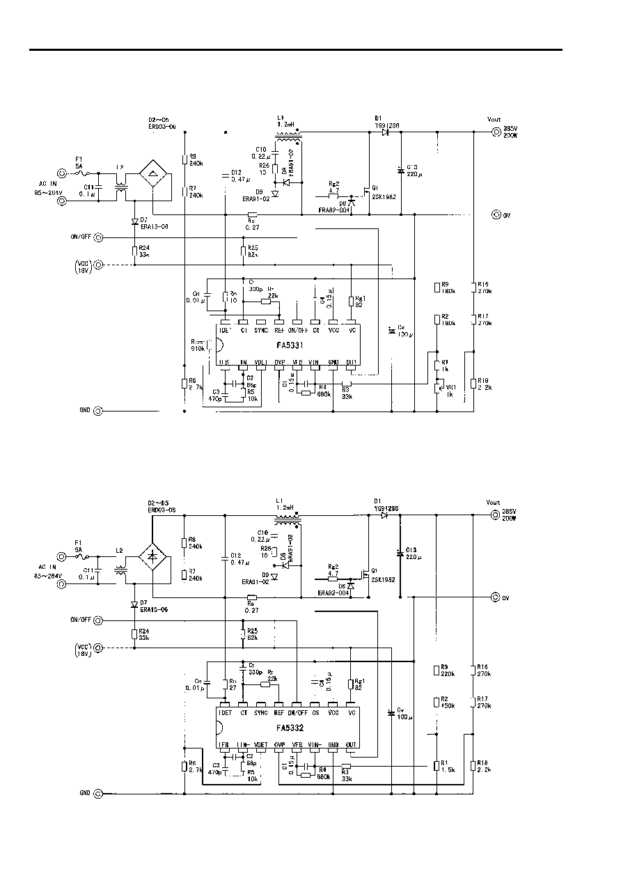
Application circuit
Example of FA5331 application circuit
Example of FA5332 application circuit
Parts tolerances characteristics are not defined in the circuit design sample shown above. When designing an actual circuit for a product, you
must determine parts tolerances and characteristics for safe and economical operation.