 | –≠–ª–µ–∫—Ç—Ä–æ–Ω–Ω—ã–π –∫–æ–º–ø–æ–Ω–µ–Ω—Ç: FA7610CP | –°–∫–∞—á–∞—Ç—å:  PDF PDF  ZIP ZIP |
FA7610CP(N)/FA7612CP(N)/FA7617CP(N)
1
s
Description
The FA7610CP(N), 7612CP(N) and 7617CP(N) are bipolar
ICs containing basic circuits necessary for PWM-type
switching power supply control.
To minimize the number of external discrete components, the
FA7610CP(N) is provided for a flyback or step-up power-
supply circuit, the FA7612CP(N) for a step-down power-supply
circuit and FA7617CP(N) for a flyback power supply circuit.
s
Features
FA7610CP(N)
∑ For flyback transformer-type or step-up power-supply circuit
(maximum output duty = 64% typical)
∑ Totem-pole predriver
∑ PWM-type switching power supply control
∑ Low-voltage operation (V
CC
= 3.6 to 22V)
∑ Latch-mode short-circuit protection function (no malfunction
by noise)
∑ Soft-start function
∑ Undervoltage lockout function
∑ One capacitor shared for short circuit protection and for soft-
start to minimize the number of external discrete components
FA7612CP(N)
∑ For step-down power-supply circuit
(maximum output duty = up to 100%)
∑ Open collector output
∑ PWM-type switching power supply control
∑ Low-voltage operation (V
CC
= 3.6 to 22V)
∑ Latch-mode short-circuit protection function (no malfunction
by noise)
∑ Soft-start function
∑ Undervoltage lockout function
∑ One capacitor shared for short circuit protection and for soft-
start to minimize the number of external discrete components
FA7617CP(N)
∑ For flyback transformer-type power-supply circuit (maximum
output duty = 67% typical)
∑ Open collector output
∑ PWM-type switching power supply control
∑ Low-voltage operation (V
CC
= 3.6 to 22V)
∑ Latch-mode short-circuit protection function (no malfunction
by noise)
∑ Soft-start function
∑ Undervoltage lockout function
∑ One capacitor shared for short circuit protection and for soft-
start to minimize the number of external discrete components
s
Applications
∑ Battery power supply for portable equipment
s
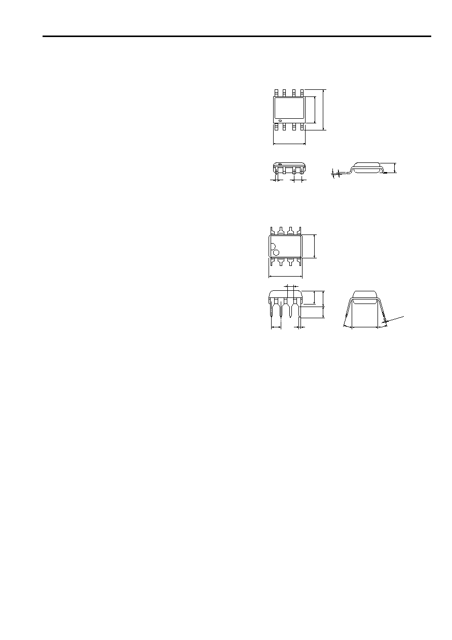
Dimensions, mm
SOP-8
4.9
3.9
6.0
±
0.2
0.4
±
0.1
1.27
±
0.2
0.20
+0.1
≠0.05
0~8
∞
1
4
8
5
1.7max
DIP-8
Bipolar IC
For Switching Power Supply Control
FA7610CP(N)/12CP(N)/17CP(N)
1
8
5
4
9.3
6.5
7.6
3.4
4.5max
1.5
3.0min
0~15∞
0~15∞
0.5
±
0.1
2.54
±
0.25
0.3
+0.1
≠0.05

FA7610CP(N)/FA7612CP(N)/FA7617CP(N)
2
s
Block diagram
FA7610CP(N)
FA7612CP(N)
FA7617CP(N)
Pin
Pin
Description
No.
symbol
1
IN (≠)
Inverting input to error amplifier
2
FB
Error amplifier output
3
GND
Ground
4
OUT
Output
5
VCC
Power supply
6
CS
Capacitor for soft-start, short-circuit protection and delay
7
CT
Oscillator timing capacitor
8
REF
Reference voltage output (2.5V)
Pin
Pin
Description
No.
symbol
1
IN (≠)
Inverting input to error amplifier
2
FB
Error amplifier output
3
GND
Ground
4
OUT
Output
5
VCC
Power supply
6
CS
Capacitor for soft-start, short-circuit protection and delay
7
CT
Oscillator timing capacitor
8
REF
Reference voltage output (2.5V)
Pin
Pin
Description
No.
symbol
1
IN (≠)
Inverting input to error amplifier
2
FB
Error amplifier output
3
GND
Ground
4
OUT
Output
5
VCC
Power supply
6
CS
Capacitor for soft-start, short-circuit protection and delay
7
CT
Oscillator timing capacitor
8
REF
Reference voltage output (2.5V)
FA7610CP(N)/FA7612CP(N)/FA7617CP(N)
3
s
Absolute maximum ratings (Ta = 25
∞
C)
Item
Symbol
Rating
Unit
FA7610C
FA7612C/17C
Supply voltage
V
CC
22
22
V
Reference voltage output current
I
OR
5
5
mA
Output current
I
O
±
50
80
mA
Total power dissipation
P
d
400
400
mW
Operating temperature
T
opr
≠20 to +85
≠20 to +85
∞
C
Storage temperature
T
stg
≠40 to +150
≠40 to +150
∞
C
s
Recommended operating conditions
Item
Symbol
FA7610C
FA7612/17C
Unit
Min.
Max.
Min.
Max.
Supply voltage
V
CC
3.6
20
3.6
20
V
Feedback resistance
R
NF
100
100
k
Oscillator timing capacitor
C
T
220
22,000
220
22,000
pF
Oscillator timing resistance
R
T
10
100
10
100
k
Oscillation frequency
f
OSC
5
200
5
500
kHz
s
Electrical characteristics (Ta = 25
∞
C, V
CC
= 6V, R
T
= 33k
, C
T
= 1000pF)
Reference voltage section Common to FA7610C/12C/17C
Item
Symbol
Test condition
Min.
Typ.
Max.
Unit
Output voltage
V
REF
I
OR
= 1mA
2.528
2.580
2.632
V
Line regulation
L
INE
V
CC
= 3.6 to 20V,
I
OR
= 1mA
4
12
mV
Load regulation
L
OAD
I
OR
= 0.1 to 1mA
1
6
mV
Output voltage variation due to temperature change
V
TC1
Ta = ≠20 to +25
∞
C
≠1
1
%
V
TC2
Ta = +25 to +85
∞
C
≠1
1
%
Oscillator section Common to FA7610C/12C/17C
Item
Symbol
Test condition
Min.
Typ.
Max.
Unit
Oscillation frequency
f
OSC
C
T
= 1000pF,
R
T
= 33k
100
111
122
kHz
Frequency variation 1 (due to supply voltage change)
f
dV
V
CC
= 3.6 to 20V
1
%
Frequency variation 2 (due to temperature change)
f
dT
Ta = ≠20 to +85
∞
C
5
%
Error amplifier section
Common to FA7610C/12C/17C
Item
Symbol
Test condition
Min.
Typ.
Max.
Unit
Reference voltage
V
B
0.515
0.525
0.535
V
Input bias current
I
B
5
100
nA
Open-loop voltage gain
A
V
70
dB
Unity-gain bandwidth
G
B
0.6
MHz
Maximam output voltage (Pin 2)
V
OM+
R
NF
= 100k
V
REF
≠0.2
V
V
OM≠
R
NF
= 100k
200
mV
Output source current (Pin 2)
I
OM+
V
OM
= 1V
40
85
200
µ
A
PWM comparator section
Item
Symbol Test condition
FA7610C
FA7612C
FA7617C
Unit
Min.
Typ.
Max.
Min.
Typ.
Max.
Min.
Typ.
Max.
Input threshold voltage (pin 2)
V
TH0
Duty cycle = 0%
0.85
0.95
0.85
0.95
0.85
0.95
V
Input threshold voltage (pin 2)
V
TH50
Duty cycle = 50%
1.1
1.1
1.1
V
Maximum duty cycle
M
(Pin 2 = 1.2V)
58
64
75
100
63
67
71
%
FA7610CP(N)/FA7612CP(N)/FA7617CP(N)
4
Soft-start circuit section
Common to FA7610C/12C/17C
Item
Symbol
Test condition
Min.
Typ.
Max.
Unit
Input bias current (Pin 6)
I
BCS
80
300
nA
Input threshold voltage (Pin 6)
V
TH CS0
Duty cycle = 0%
0.22
0.32
V
Input threshold voltage (Pin 6)
V
TH CS50
Duty cycle = 50%
0.46
V
Short-circuit protection circuit section
Common to FA7610C/12C/17C
Item
Symbol
Test condition
Min.
Typ.
Max.
Unit
Input threshold voltage (Pin 2)
V
TH PC
1.20
1.50
1.80
V
Charge current (Pin 6)
I
CHG
Pin 6 = 0V, Pin 2 = 2V
20
30
40
µ
A
Latch-mode threshold voltage (Pin 6)
V
TH LA
1.20
1.50
1.80
V
Undervoltage lockout circuit section
Common to FA7610C/12C/17C
Item
Symbol
Test condition
Min.
Typ.
Max.
Unit
OFF-to-ON threshold voltage
V
TH ON
2.70
V
ON-to-OFF threshold voltage
V
TH OFF
2.52
V
Voltage hysteresis
V
HYS
60
180
mV
Output section
Item
Symbol
Test condition
FA7610C
FA7612C/17C
Unit
Min.
Typ.
Max.
Min.
Typ.
Max.
H-level output voltage (Pin 4)
V
OH
R
L
= 10k
3.5
4.0
--
--
--
V
L-level output voltage (Pin 4)
V
OL
Output sink
0.25
0.65
0.9
1.5
V
current = 20mA
Output source current (Pin 4)
I
SOURCE
Pin 4 = 0V
8
11
14
--
--
--
mA
Overall device
Item
Symbol
Test condition
FA7610C
FA7612C/17C
Unit
Min.
Typ.
Max.
Min.
Typ.
Max.
Supply current
I
CC LA
Latch mode
1.6
2.2
1.5
2.2
mA
Operating-state supply current
I
CC AV
R
L
=
2.6
3.8
1.8
3.0
mA
Duty cycle = 50%
FA7610CP(N)/FA7612CP(N)/FA7617CP(N)
5
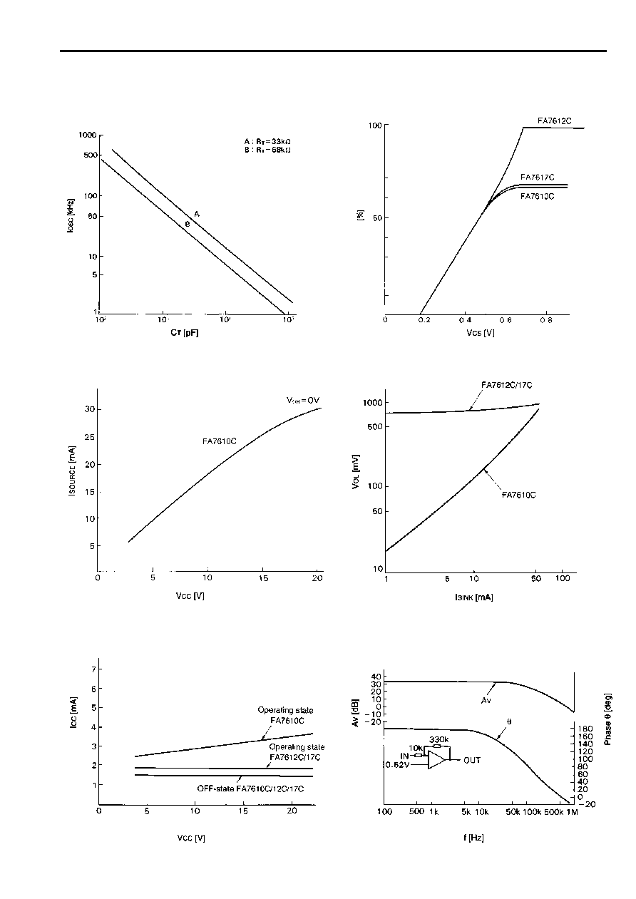
s
Characteristic curves (Ta = 25
∞
C)
Oscillation frequency(f
OSC
) vs.
Output duty cycle vs. CS terminal voltage(V
CS
)
timing capacitor capacitance(C
T
)
Output source current (I
source
) vs.
L-level output voltage(V
OL
) vs. output sink current
supply voltage(V
CC
)
(I
SINK
)
Supply current(I
CC
) vs. supply voltage(V
CC
)
Error amplifier frequency(f) vs. voltage gain(AV) / phase (
)