 | –≠–ª–µ–∫—Ç—Ä–æ–Ω–Ω—ã–π –∫–æ–º–ø–æ–Ω–µ–Ω—Ç: FA7615CPE | –°–∫–∞—á–∞—Ç—å:  PDF PDF  ZIP ZIP |
FA7615CP(E)
1
s
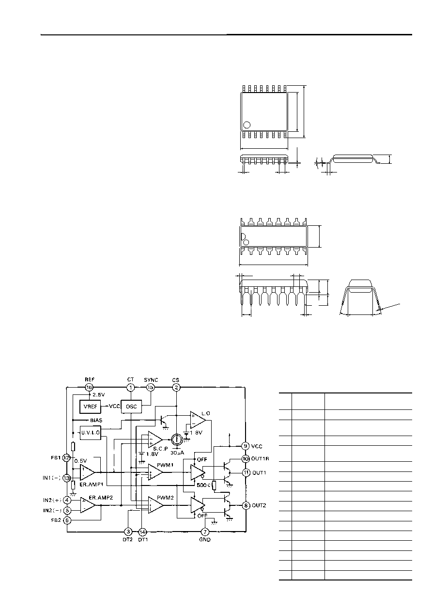
Description
The FA7615CP(E) is a bipolar IC containing basic circuit
necessary for PWM-type switching power supply control. This
IC can be operated by external synchronizing pulses.
s
Features
∑ External synchronization input terminal
∑ Low-voltage operation (V
CC
= 3.6 to 22V)
∑ Totem-pole predriver
∑ Latch-mode short-circuit protection function (no malfunction
due to electrical noise)
∑ One capacitor shared for short-circuit protection and for soft-
start to minimize the number of external discrete components
s
Applications
∑ Battery power supply for portable equipment
s
Dimensions, mm
SSOP-16
1
8
9
16
0.6
0~10∞
0.65
7.9
±
0.3
5.3
6.2
0.1
±
0.1
0.2
+0.1
≠0.05
0.3
2.1max
DIP-16
s
Block diagram
FA7615CP(E)
Bipolar IC
For Switching Power Supply Control
Pin
Pin
Description
No.
symbol
1
CT
Oscillator timing capacitor
2
CS
Capacitor for soft-start,
short-circuit protection and delay
3
DT2
Dead time adjustment
4
IN2 (+)
Non-inverting input to error
amplifier
5
IN2 (≠)
Inverting input to error amplifier
6
FB2
Error amplifier output
7
GND
Ground
8
OUT2
CH. 2 Output
9
VCC
Power supply
10
OUT1R
CH. 1 Current limiting resistor
11
OUT1
CH. 1 Output
12
FB1
Error amplifier output
13
IN1 (≠)
Inverting input to error amplifier
14
DT1
Dead time adjustment
15
SYNC
External synchronization input
16
REF
Reference voltage output (2.5V)
1
16
9
8
19.4
6.5
7.6
3.4
4.3max
1.5
0.81
3.1min
0.2min
0~15∞
0~15∞
0.5
±
0.1
2.54
±
0.25
0.3
+0.1
≠0.05
FA7615CP(E)
2
s
Electrical characteristics (Ta = 25
∞
C, V
CC
= 6V, R
T
= 47k
, C
T
= 1000pF)
Reference voltage section
Item
Symbol
Test condition
Min.
Typ.
Max.
Unit
Output voltage
V
REF
I
OR
= 1mA
2.383
2.432
2.481
V
Line regulation
L
INE
V
CC
= 3.6 to 20V, I
OR
= 1mA
4
12
mV
Load regulation
L
OAD
I
OR
= 0.1 to 1mA
1
6
mV
Output voltage variation due to temperature change
V
TC1
Ta = ≠20 to +25
∞
C
≠1
1
%
V
TC2
Ta = +25 to +85
∞
C
≠1
1
%
Oscillator section
Item
Symbol
Test condition
Min.
Typ.
Max.
Unit
Oscillation frequency
f
OSC
C
T
= 1000pF,
R
T
= 47k
17
20
23
kHz
Frequency variation 1 (due to supply voltage change)
f
dV
V
CC
= 3.6 to 20V
1
%
Frequency variation 2 (due to temperature change)
f
dT
Ta = ≠20 to +85
∞
C
5
%
Synchronizing terminal input current
I
SYNC
V
SYNC
= 2V
0.4
1.0
mA
Synchronizing terminal input voltage
V
SYNC
1
2.5
V
Error amplifier section
Item
Symbol
Test condition
Min.
Typ.
Max.
Unit
Reference voltage
V
B
0.484
0.494
0.504
V
Input bias current
I
B
5
100
nA
Open-loop voltage gain
A
V
70
dB
Unity-gain bandwidth
G
B
1.0
MHz
Maximum output voltage (Pin 6 and Pin 12)
V
OM+
R
NF
= 100k
V
REF
≠0.2
V
V
OM≠
R
NF
= 100k
200
mV
Output source current (Pin 6 and Pin 12)
I
OM+
V
OM
= 1V
40
85
200
µ
A
PWM comparator section
Item
Symbol
Test condition
Min.
Typ.
Max.
Unit
Input threshold voltage (Pin 6 and Pin 12)
V
TH0
Duty cycle = 0%
0.38
0.48
V
Input threshold voltage (Pin 6 and Pin 12)
V
TH50
Duty cycle = 50%
0.6
V
s
Absolute maximum ratings
Item
Symbol
Rating
Unit
Supply voltage
V
CC
22
V
Reference voltage output current
I
OR
5
mA
Output current
I
O
±
50
mA
Total power dissipation
P
d
400
mW
Operating temperature
T
opr
≠20 to +85
∞
C
Storage temperature
T
stg
≠40 to +150
∞
C
s
Recommended operating conditions
Item
Symbol
Min.
Max.
Unit
Supply voltage
V
CC
3.6
20
V
Feedback resistance
R
NF
100
k
Oscillator timing capacitor
C
T
220
22,000
pF
Oscillator timing resistance
R
T
10
100
k
Oscillation frequency
f
OSC
5
200
kHz
FA7615CP(E)
3
Dead time adjustment circuit section
Item
Symbol
Test condition
Min.
Typ.
Max.
Unit
Input bias current (Pin 3 and Pin 14)
I
BDT
80
300
nA
Input threshold voltage (Pin 3 and Pin 14)
V
TH DT0
Duty cycle = 0%
0.38
0.48
V
Input threshold voltage (Pin 3 and Pin 14)
V
TH DT50
Duty cycle = 50%
0.60
V
Short-circuit protection circuit section
Item
Symbol
Test condition
Min.
Typ.
Max.
Unit
Input threshold voltage (Pin 6 and Pin 12)
V
TH PC
1.60
1.80
2.00
V
Charge current (Pin 2)
I
CHG
Pin 2 = 0V, Pin 6, Pin 12 = 2V 18
30
42
µ
A
Latch-mode threshold voltage (Pin 2)
V
TH LA
1.60
1.80
2.00
V
Undervoltage lockout section
Item
Symbol
Test condition
Min.
Typ.
Max.
Unit
OFF-to-ON threshold voltage
V
TH ON
2.65
V
ON-to-OFF threshold voltage
V
TH OFF
2.60
V
Voltage hysteresis
V
HYS
50
mV
Output section
Item
Symbol
Test condition
Min.
Typ.
Max.
Unit
Output saturation voltage
H-level (CH.1)
V
O1H
Output source current = 20mA
0.3
0.8
V
L-level (Common to CH.1 and CH.2)
V
O1L/2L
Output sink current = 20mA
0.3
0.8
V
CH. 1 Output source current (Pin 11)
I
SOURCE1
Pin 11 = 0V
6
11
15
mA
CH. 2 Output source current (Pin 8)
I
SOURCE2
V
CC
= 16V, Pin 8 = 0V
19
27
36
mA
Overall device
Item
Symbol
Test condition
Min.
Typ.
Max.
Unit
Supply current
I
CC LA
Latch mode
2.0
3.0
mA
Operating-state supply current
I
CC AV
R
L
=
Duty cycle = 50%
3.5
6.0
mA
FA7615CP(E)
4
s
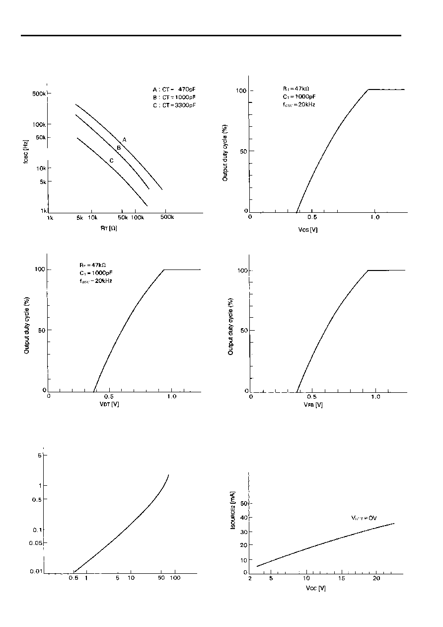
Characteristic curves (Ta = 25
∞
C)
Oscillation frequency (f
OSC
) vs.
Output duty cycle vs. CS terminal voltage (V
CS
)
timing resistor resistance (R
T
)
Output duty cycle vs. DT terminal voltage (V
DT
)
Output duty cycle vs. FB terminal voltage (V
FB
)
H-level output saturation voltage (V
O1H
)
CH-2 output source current (I
SOURCE2
)
vs. CH. 1 output source current (I
SOURCE1
)
vs. supply voltage (V
CC
)
V
O1H
[V]
I
SOURCE
[mA]
FA7615CP(E)
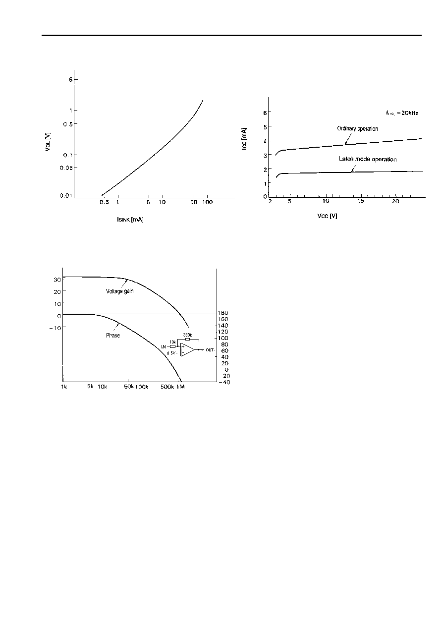
5
L-level output voltage (V
OL
) vs. output sink current (I
SINK
)
Supply current (I
CC
) vs. supply voltage (V
CC
)
Error amplifier frequency (f) vs. voltage gain (AV)/phase (
)
A
V
[dB]
f [Hz]
Phase
[deg]
FA7615CP(E)
6
s
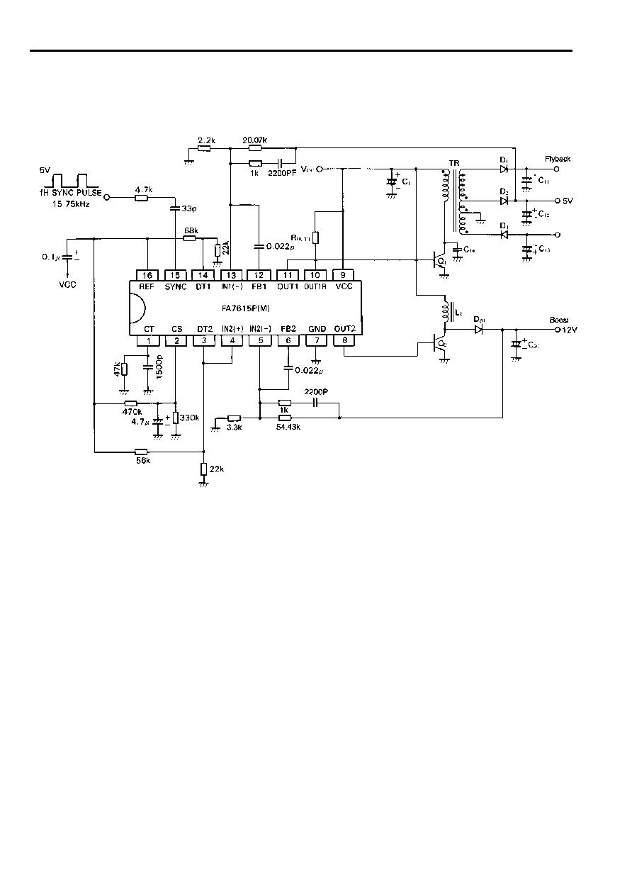
Application circuit
Flyback-transformer type and
chopper type boost converter circuit
Parts tolerances characteristics are not defined in the circuit design
sample shown above. When designing an actual circuit for a product,
you must determine parts tolerances and characteristics for safe and
economical operation.
Please connect a capacitor, which the value is about 0.01
µ
F to 0.1
µ
F,
between VCC
and REF terminals in order to prevent from irregular
output pulse at start-up.