 | –≠–ª–µ–∫—Ç—Ä–æ–Ω–Ω—ã–π –∫–æ–º–ø–æ–Ω–µ–Ω—Ç: FA7616CP | –°–∫–∞—á–∞—Ç—å:  PDF PDF  ZIP ZIP |
FA7616CP(E)(V)
1
s
Description
The FA7616CP(E)(V) is a bipolar control IC having two
channels of PWM-type switching regulator control circuits.
With this IC, a DC-to-DC converter can be easily implemented
for a minimum input voltage of 1.4V.
s
Features
∑ Input voltage from 1.4V (V
CC
= 1.4 to 12V)
∑ Open-collector output
∑ Wide operating frequency range (f
OSC
: 10 to 500kHz)
∑ Output ON/OFF control function
∑ Not many external discrete components are needed
s
Applications
∑ Battery power supply (two, 1.5V batteries) for portable
equipment
s
Dimensions, mm
TSSOP-16
1
8
9
16
0.6
0~10∞
0.65
6.4
±
0.2
4.4
±
0.1
5.0
±
0.1
0.1
±
0.1
0.15
+0.05
≠0.06
0.24
+0.08
≠0.07
1.2max
SSOP-16
1
8
9
16
0.6
0~10∞
0.65
7.9
±
0.3
5.3
6.2
0.1
±
0.1
0.2
+0.1
≠0.05
0.3
2.1max
DIP-16
1
16
9
8
19.4
6.5
7.6
3.4
4.3max
1.5
0.81
3.1min
0.2min
0~15∞
0~15∞
0.5
±
0.1
2.54
±
0.25
0.3
+0.1
≠0.05
s
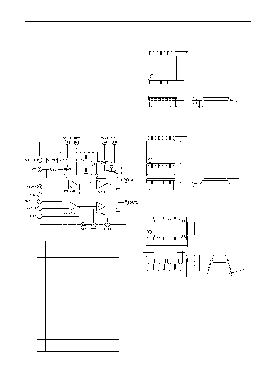
Block diagram
FA7616CP(E)(V)
Bipolar IC
For Switching Power Supply Control
Pin
Pin
Description
No.
symbol
1
VCC2
IC main power supply
2
CT
Oscillator timing capacitor
3
IN2 (+)
Non-inverting input to error
amplifier
4
IN2 (≠)
Inverting input to error amplifier
5
FB2
Error amplifier output
6
DT2
Dead time adjustment
7
OUT2
CH. 2 Output
8
GND
Ground
9
OUT1
CH. 1 Output
10
DT1
Dead time adjustment
11
FB1
Error amplifier output
12
IN1 (≠)
Inverting input to error amplifier
13
CST
Start-up circuit timing capacitor
14
VCC1
Start-up circuit power supply
15
ON/OFF
Output ON/OFF control
16
REF
Reference voltage output (1.20V)

FA7616CP(E)(V)
2
s
Electrical characteristics (Ta = 25
∞
C, V
CC1
= 1.6V, V
CC2
= 3V, V
15
= 2V, C
T
= 1000pF, R
T
= 10k
)
Reference voltage section
Item
Symbol
Test condition
Min.
Typ.
Max.
Unit
Output voltage
V
REF
I
OR
= 0.1mA
1.196
1.220
1.244
V
Line regulation
L
INE
V
CC
= 2.5 to 12V, V
15
= 2V fixed
1
8
mV
Load regulation
L
OAD
I
OR
= 0.1 to 1mA
1
8
mV
Output voltage variation due to temperature change
V
TC1
Ta = ≠20 to +25
∞
C
≠2
≠0.3
1
%
I
OR
= 0.1mA
V
TC2
Ta = +25 to +85
∞
C
≠2
≠0.6
1
%
I
OR
= 0.1mA
Oscillator section
Item
Symbol
Test condition
Min.
Typ.
Max.
Unit
Oscillation frequency
f
OSC
C
T
= 1000pF,
R
T
= 10k
80
92
110
kHz
Frequency variation 1 (due to supply voltage change)
f
dV
V
CC
= 2.5 to 12V
1
3
%
Frequency variation 2 (due to temperature change)
f
dT
Ta = ≠20 to +85
∞
C
2
%
Error amplifier section
Item
Symbol
Test condition
Min.
Typ.
Max.
Unit
Input offset voltage
V
IO
2
10
mV
Input bias current
I
B
1
µ
A
Common-mode input voltage
V
CM
0
V
CC2
≠1.7 V
Open-loop voltage gain
A
V
70
dB
Unity-gain bandwidth
G
B
1.0
MHz
Maximum output voltage
V
OM+
R
NF
= 100k
V
CC2
≠0.5
V
V
OM≠
R
NF
= 100k
200
mV
Output source current
I
OM+
V
OM
= 1V
40
85
170
µ
A
PWM comparator section
Item
Symbol
Test condition
Min.
Typ.
Max.
Unit
Input threshold voltage
V
TH0
Duty cycle = 0%
0.80
V
Input threshold voltage
V
TH100
Duty cycle = 100%
1.45
V
s
Absolute maximum ratings
Item
Symbol
Rating
Unit
Supply voltage
V
CC
12
V
Reference voltage output current
I
OR
5
mA
Output sink current
I
O
10
mA
Total power dissipation
P
d
300
mW
Operating temperature
T
opr
≠20 to +85
∞
C
Storage temperature
T
stg
≠40 to +150
∞
C
s
Recommended operating conditions
Item
Symbol
Min.
Max.
Unit
Supply voltage 1
V
CC1
1.4
12
V
Supply voltage 2
V
CC2
2.5
12
V
Output sink current (at start-up)
I
SINK
3
mA
Output sink current
I
SINK
5
mA
(at steady state)
Oscillation frequency
f
OSC
10
500
kHz
Oscillator timing capacitor
C
ST
47
10,000
pF
(start-up circuit)
Oscillator timing capacitor
C
T
220
10,000
pF
Oscillator timing resistance
R
T
4.7
47
k
Feedback resistance
R
NF
100
k
FA7616CP(E)(V)
3
Dead time adjustment circuit section
Item
Symbol
Test condition
Min.
Typ.
Max.
Unit
Input threshold voltage
V
TH DT0
Duty cycle = 0%
0.08
0.15
V
Input threshold voltage
V
TH DT100
Duty cycle = 100%
0.80
0.95
V
Output ON/OFF circuit section
Item
Symbol
Test condition
Min.
Typ.
Max.
Unit
ON/OFF threshold voltage
V
TH ON
0.5
0.9
1.2
V
Input current
I
I ON
Pin 15 = 2V
650
850
µ
A
Start-up circuit section
Item
Symbol
Test condition
Min.
Typ.
Max.
Unit
Oscillation frequency
f
SC
C
ST
= 1000pF,
V
CC2
= 0.5V
70
95
115
kHz
ON duty cycle
D
ST
C
ST
= 1000pF,
V
CC2
= 0.5V
40
50
60
%
Threshold voltage to stop
V
CC2 TH
ON-to-OFF threshold voltage 2.15
2.30
2.45
V
at start-up circuit
Output section
Item
Symbol
Test condition
Min.
Typ.
Max.
Unit
Output leakage current
I
LEAK
V
O
= 12V
5
µ
A
L-level output voltage
V
OL
Output sink current =5mA
0.25
0.55
V
Overall device
Item
Symbol
Test condition
Min.
Typ.
Max.
Unit
Standby current 1
I
CC ST1
Pin 15 = 0V or
V
CC2
> 2.45V
0.1
10
µ
A
Standby current
I
CC STAR
Pin 15 = 2V,
V
CC2
< 2.15V
400
800
µ
A
Standby current 2
I
CC ST2
Pin 15 = 0V,
V
CC2
= 3V
0.4
0.7
mA
Operating-state supply current
I
CC AV
Pin 15 = 2V,
V
CC2
= 3V
2.2
3.2
mA
s
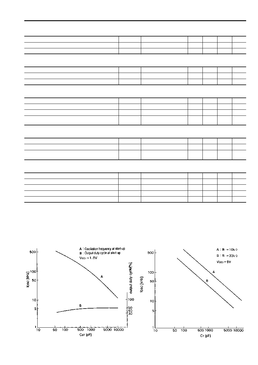
Characteristic curves (Ta = 25
∞
C)
Oscillation frequency (f
OSC
) vs.
Oscillation frequency (f
OSC
) vs. timing capacitor capacitance (C
T
)
timing capacitor capacitance (C
ST
) and output duty cycle
At steady state
At strat-up state
FA7616CP(E)(V)
4
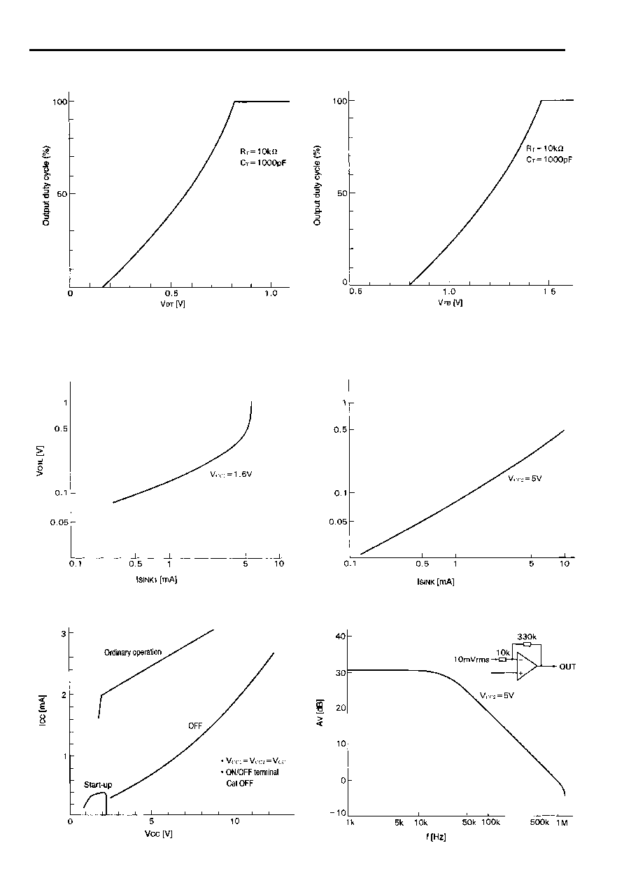
Output duty cycle vs. DT terminal voltage (V
DT
)
Output duty cycle vs. FB terminal voltage (V
FB
)
L-level output voltage (V
O1L
) vs. CH. 1 output sink current
L-level output voltage (V
OL
) vs. output sink current
(I
SINK1
)
(I
SINK
)
At start-up state
At steady state
Supply current (I
CC
) vs. supply voltage (V
CC
)
Error amplifier frequency (f) vs. voltage gain (A
V
)
V
OL
[V]
FA7616CP(E)(V)
5
s
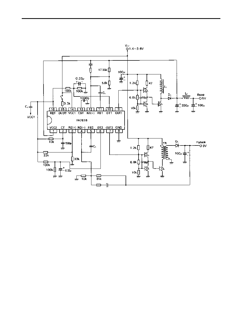
Application circuit
Flyback-transformer type and chopper type boost converter circuit
Parts tolerances characteristics are not defined in the circuit design
sample shown above. When designing an actual circuit for a product,
you must determine parts tolerances and characteristics for safe and
economical operation.
Please connect a capacitor, which the value is about 0.01
µ
F to 0.1
µ
F,
between VCC
and REF terminals in order to prevent from irregular
output pulse at start-up.