 | –≠–ª–µ–∫—Ç—Ä–æ–Ω–Ω—ã–π –∫–æ–º–ø–æ–Ω–µ–Ω—Ç: FA7700V | –°–∫–∞—á–∞—Ç—å:  PDF PDF  ZIP ZIP |
FA7700V, FA7701V
1
s
Block diagram
FA7700V
FA7701V
FA7700V, FA7701V
s
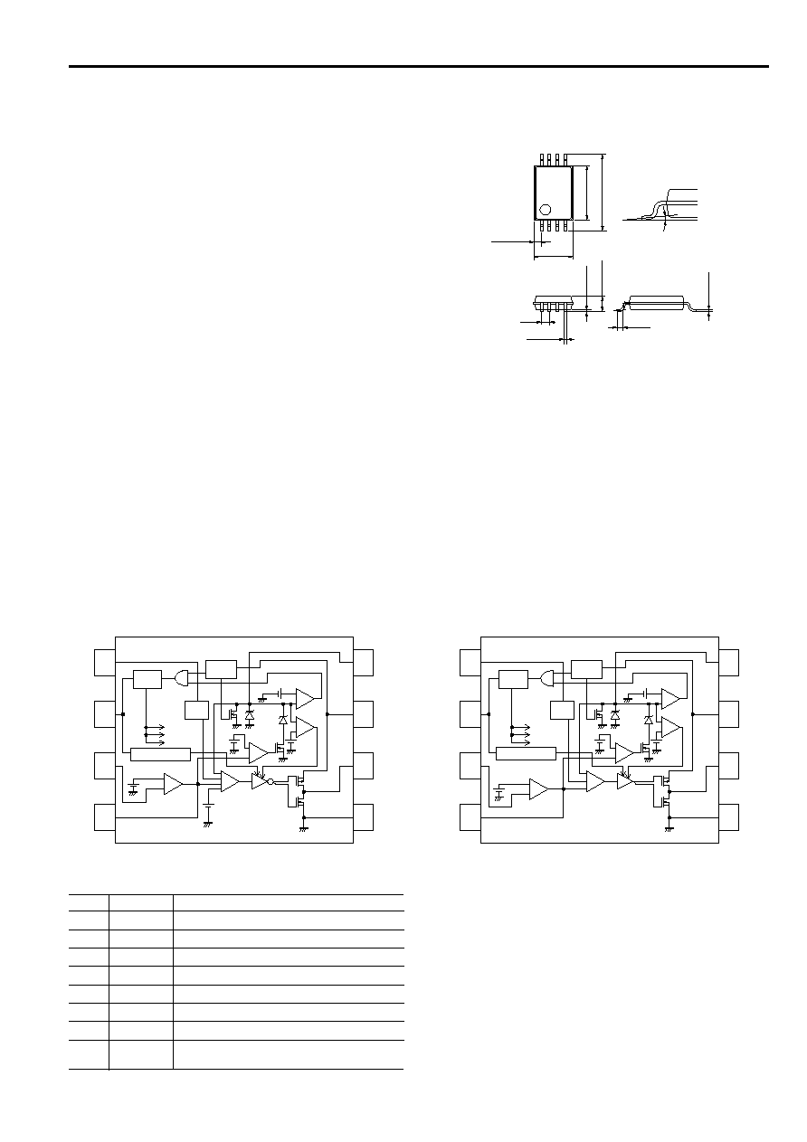
Dimensions, mm
TSSOP-8
±
0.2
4.4
±
0.3
6.4
1
0
t
o
0
∞
±
0.3
3.1
±
0.1
0.15
±
0.05
0.1
1.30 max
±
0.1
0.22
±
0.2
0.5
0.65
0.575 typ
s
Description
FA7700V/FA7701V are the PWM type DC to DC converter
control ICs with 1ch output that can directly drive power
MOSFETs. CMOS devices with high breakdown voltage are
used in these ICs and low power consumption is achieved.
These ICs have not only the functions equivalent to those of
FA76XX series but also the functions of directly driving Nch/Pch
MOSFETs, lower power consumption, higher frequency
operation, and less external components.
s
Features
∑ Wide range of supply voltage: V
CC
=2.5 to 20V
∑ FA7700V: For boost, flyback converter
(Maximum output duty cycle is 80%)
∑ FA7701V: For buck converter
(Maximum output duty cycle is 100%)
∑ Output stage consist of CMOS push-pull circuit, and achieves
a high speed switching of external MOSFETs. (FA7700V: For
Nch-MOSFET driving, FA7701V: For Pch-MOSFET driving)
∑ High accuracy reference voltage (Error amplifier): 0.88V
±
2%
∑ Soft start function
∑ Adjustable built-in timer latch for short-circuit protection
∑ Output ON/OFF control function
∑ Less external discrete components needed (2 components
less than conventional version of the equivalent products)
∑ Low power consumption
Stand-by current: 40
µ
A typ.
Operating current: 1.2mA typ. (Including error amplifier output
current and oscillator current)
∑ High frequency operation: 50kHz to 1MHz
∑ Package: TSSOP-8, thin and small
Pin No. Pin symbol Description
1
RT
Oscillator timing resistor
2
REF
Internal bias voltage
3
IN (≠)
Error amplifier inverting input
4
FB
Error amplifier output
5
GND
Ground
6
OUT
Output for driving switching device
7
VCC
Power supply
8
CS
ON/OFF, soft start, timer latched short
circuit protection
RT
REF
V R E F
O S C
BIAS
U V L O
5.5V
≠
+
OFF
4
FB
IN≠
+
≠
+
P W M
≠
+
ON/OFF
S.C.DET
0.3V
1.5V
1.5V
≠
+
S.C.P
2.2V
VREF
Power Good Signal
ON/OFF
1
2
3
8
7
6
5
CS
VCC
OUT
GND
≠
+
0.88V
E R . A M P
+
2.2V
+
≠
+
P W M
≠
+
E R . A M P
ON/OFF
V R E F
O S C
BIAS
U V L O
5.5V
≠
+
≠
+
ON/OFF
S.C.DET
0.3V
1.5V
1.5V
≠
+
S.C.P
2.2V
OFF
RT
REF
4
FB
IN≠
1
2
3
8
7
6
5
CS
VCC
OUT
GND
0.88V
Power Good Signal
VREF
2.2V
CMOS IC
For Switching Power Supply Control
FA7700V, FA7701V
2
s
Absolute maximum ratings
Maximum power dissipation curve
I
tem
Symbol
Rating
Unit
Power supply voltage
Vcc
20
V
REF terminal output current
I
REF
2
mA
OUT terminal source current
I
SO peak
≠400 (peak)
mA
I
SO cont
≠50 (continuos)
OUT terminal sink current
I
SI peak
+150 (peak)
mA
I
SI cont
+50 (continuos)
RT, REF, IN≠, FB terminal voltage
V
RT
, V
REF
+2.5 (max.)
V
V
IN≠
, V
FB
≠0.3 (min.)
CS terminal voltage
V
CS
Self limiting 5.5 (max.)
V
≠0.3 (min.)
CS terminal sink current
I
CS
200
µ
A
Power dissipation
Pd
250 (Ta 25∞C)
mW
Operating ambient temperature
Ta
≠30 to +85
∞C
Operating junction temperature
Tj
+125
∞C
Storage temperature
T
stg
≠40 to +150
∞C
≠30
30
90
60
0
125
150
0
Ambient temperature [∞C]
Max.
po
w
e
r
dissipation [mW]
50
100
150
200
250
300
s
Recommended operating condition
Item
Symbol
Min.
Typ.
Max.
Unit
Supply voltage
V
CC
2.5
6
18
V
DC feedback resistor of error amplifier
R
NF
100
k
VCC terminal capacitance
C
VCC
0.1
µ
F
REF terminal capacitance
C
REF
0.047
0.1
1
µ
F
CS terminal capacitance
C
S
0.01
10
µ
F
CS terminal sink current
I
csin
1*
50
µ
A
Oscillation frequency
f
osc
50
1000
kHz
* Lower limit of I
CSIN
does not include leak current "I
L
" for capacitor Cs. Set a
resistor "R
CS
[M
]" connected between VCC terminal and CS terminal to
satisfy the equation.
V
CC
≠ 1.5
R
CS
[M
]
V
CC
≠ 1.5
50
µ
A + I
L
1
µ
A + I
L
FA7700V, FA7701V
3
Pulse width modulation (PWM) section (FB terminal voltage and duty cycle)
Item
Symbol
Test condition
Min.
Typ.
Max.
Unit
FB 0% threshold
V
FB0
Duty cycle = 0%
0.560
0.660
0.760
V
FB 50% threshold
V
FB50
Duty cycle = 50%
0.880
V
Maximum duty cycle
FA7700
D
MAX1
R
T
=100k
, f=50kHz
85
90
95
%
D
MAX2
R
T
=22k
, f 185kHz
83
88
93
%
D
MAX3
R
T
=3k
, f 1MHz
80
86
92
%
FA7701
D
MAX
100
%
Error amplifier section (IN- terminal, FB terminal)
Item
Symbol
Test condition
Min.
Typ.
Max.
Unit
Reference voltage
V
B
IN- terminal, FB terminal:
0.863
0.880
0.897
V
Shorted (voltage follower)
Input current
I
IN≠
-500
+500
nA
V
B
line regulation
V
BLINE
Vcc=2.5 to 20V
±
1
±
5
mV
V
B
variation with temperature
V
BTC1
Ta=≠30 to 25
∞
C
±
0.3
%
V
BTC2
Ta=25 to 85
∞
C
±
0.3
%
Open loop gain
A
VO
70
dB
Unity gain bandwidth
f
T
1.5
MHz
Output current
Source
I
OHE
FB terminal=V
REF
≠ 0.5V
≠220
≠160
≠100
µ
A
Sink
I
OLE
FB terminal=0.5V
3
6
12
mA
Oscillator section (Frequency set by R
T
terminal)
Item
Symbol
Test condition
Min.
Typ.
Max.
Unit
Oscillation frequency
f
osc
R
T
=22k
155
185
215
kHz
Line regulation
f
LINE
Vcc=2.5 to 20V
±
0.1
%
Variation with temperature
f
TC1
Ta=≠30 to 25
∞
C, 50k to 1MHz
±
2
%
f
TC2
Ta=25 to 85
∞
C, 50k to 1MHz
±
3
%
s
Electrical characteristics (Ta=25∞C, V
CC
=6V, R
T
=22k
)
Internal bias section (REF terminal voltage)
Item
Symbol
Test condition
Min.
Typ.
Max.
Unit
Output voltage
V
REF
REF terminal source current
2.16
2.23
2.30
V
I
REF
=0mA
Line regulation
V
LINE
Vcc=2.5 to 20V, I
REF
=0mA
±
2
±
14
mV
Load regulation
V
LOAD
I
REF
=0 to 2mA
±
2
±
12
mV
Variation with temperature
V
TC1
Ta=≠30 to 25
∞
C
±
0.3
%
V
TC2
Ta=25 to 85
∞
C
±
0.3
%
Undervoltage lock-out section (V
CC
terminal voltage)
Item
Symbol
Test condition
Min.
Typ.
Max.
Unit
ON threshold
V
CCON
2.07
2.30
V
OFF threshold
V
CCOF
1.60
1.93
V
Hysteresis voltage
V
CCHY
0.04
0.14
0.24
V
Variation with temperature
V
CCHY
Ta= ≠30 to 25
∞
C
+0.2
mV/
∞
C
Ta= 25 to 85
∞
C
≠0.2
mV/
∞
C
FA7700V, FA7701V
4
Soft start section (CS terminal voltage)
Item
Symbol
Test condition
Min.
Typ.
Max.
Unit
Threshold voltage 1
V
CS0
Duty cycle=0%
0.560
0.660
0.760
V
Threshold voltage 2
V
CS50
Duty cycle=50%
0.880
V
ON/OFF section (CS terminal voltage)
Item
Symbol
Test condition
Min.
Typ.
Max.
Unit
ON/OFF threshold
V
ONOF
0.150
0.300
0.450
V
Threshold variation with temperature
V
ONTC
Ta = ≠30 to 85
∞
C
+0.5
mV/
∞
C
Timer latched short circuit protection section (FB terminal, CS terminal)
Item
Symbol
Test condition
Min.
Typ.
Max.
Unit
Short detection threshold voltage
V
FBTH
FB terminal voltage
1.350
1.500
1.650
V
Latched mode threshold voltage
V
CSTH
CS terminal voltage
2.050
2.200
2.350
V
Latched mode reset voltage
V
CSRE
CS terminal voltage
1.700
2.030
2.300
V
Latched mode hysteresis
V
CSHY
CS terminal voltage
50
170
350
mV
CS terminal clamped voltage
V
CSCL1
FB terminal<1.35V, CS sink current= +1
µ
A
1.400
1.500
1.600
V
V
CSCL2
FB terminal>1.65V, CS sink current= +150
µ
A
4.500
5.500
6.500
V
Overall section (Supply current to VCC terminal)
Item
Symbol
Test condition
Min.
Typ.
Max.
Unit
OFF mode supply current
I
CCST1
CS terminal=0V
40
100
µ
A
Operating mode supply current
I
CC0
Duty cycle=0%, OUT:Open, IN≠=0V, FB:Open
0.9
1.5
mA
I
CC1
Duty cycle=50%, OUT:Open, IN≠, FB:Shorted
1.2
2.0
mA
Latched mode supply current
I
CCLAT
CS terminal >2.35V, IN≠=0V, FB:Open
0.9
1.5
mA
Output stage section (OUT terminal)
Item
Symbol
Test condition
Min.
Typ.
Max.
Unit
High side on resistance
R
ONH
VCC=6V, source current= ≠50mA
10
20
R
ONH
VCC=2.5V, source current= ≠50mA
18
36
Low side on resistance
R
ONL
VCC=6V, sink current= +50mA
5
10
R
ONL
VCC=2.5V, sink current= +50mA
5
10
Rise time
FA7700
tr
330pF load to GND terminal
20
ns
FA7701
330pF load to VCC terminal
25
ns
Fall time
FA7700
tf
330pF load to GND terminal
45
ns
FA7701
330pF load to VCC terminal
40
ns
FA7700V, FA7701V
5
s
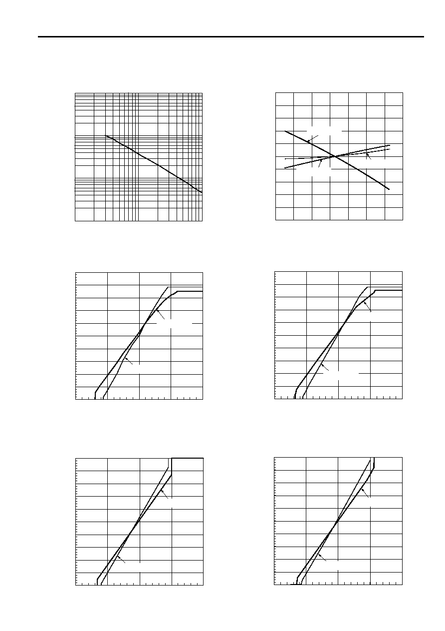
Characteristic curves
Oscillation frequency (f
OSC
) vs.
Oscillation frequency (f
OSC
) vs. ambient temperature
timing resistor resistance (R
T
)
Duty cycle vs. FB terminal voltage
Duty cycle vs. CS terminal voltage
FA7700
FA7700
Duty cycle vs. FB terminal voltage
Duty cycle vs. CS terminal voltage
FA7701
FA7701
1
10
100
10
100
1000
10000
Timing resisitor R
T
[k
]
Oscillation frequency [kHz]
Ambient temperature Ta [∞C]
Oscillation frequency v
a
r
i
ation [%]
≠40
≠20
0
20
40
60
80
100
≠5
≠4
≠3
≠2
≠1
0
1
2
3
4
5
fosc=1MHz
fosc=50kHz
fosc=185kHz
FB terminal voltage [V]
Duty cycle [%]
0.5
0.7
0.9
1.1
1.3
100
90
80
70
60
50
40
30
20
10
0
fosc=1MHz
fosc=185kHz
CS terminal voltage [V]
Duty cycle [%]
0.5
0.7
0.9
1.1
1.3
100
90
80
70
60
50
40
30
20
10
0
fosc=1MHz
fosc=185kHz
Duty cycle [%]
0.5
0.7
0.9
1.1
1.3
100
90
80
70
60
50
40
30
20
10
0
FB terminal voltage [V]
fosc=1MHz
fosc=185kHz
Duty cycle [%]
0.5
0.7
0.9
1.1
1.3
100
90
80
70
60
50
40
30
20
10
0
CS terminal voltage [V]
fosc=1MHz
fosc=185kHz
FA7700V, FA7701V
6
Maximum duty cycle vs. ambient temperature
Error amp. reference voltage vs. ambient temperature
FA7700
Internal bias voltage vs. ambient temperature
Undervoltage lock-out vs. ambient temperarure
CS terminal ON/OFF threshold vs.
CS terminal voltage vs. CS terminal sink current
ambient temperature
≠40
≠20
0
20
40
60
80
100
94
92
90
88
86
84
82
80
Ambient temperature Ta [∞C]
Max.
duty cycle [%]
fosc=1MHz
fosc=50kHz
fosc=185kHz
0.86
≠40
≠20
0
20
40
60
80
100
Ambient temperature Ta [∞C]
Ref
erence v
o
ltage [V]
0.87
0.88
0.89
0.90
2.18
≠20
≠40
0
20
40
60
80
100
Ambient temperature Ta [∞C]
Inter
nal bias v
o
ltage [V]
2.20
2.22
2.24
2.26
2.28
Vcc
ON
Vcc
OFF
1.80
≠20
≠40
0
20
40
60
80
100
Ambient temperature Ta [∞C]
Vcc ter
m
inal ON/OFF threshold
1.85
1.90
1.95
2.00
2.20
2.15
2.10
2.05
0.15
≠20
≠40
0
20
40
60
80
100
Ambient temperature Ta [∞C]
CS ter
m
inal ON/OFF threshold
0.20
0.25
0.30
0.35
0.40
20
0
1
2
3
4
5
6
7
CS terminal voltage [V]
40
60
80
100
120
0
140
160
180
200
CS ter
m
inal sink current [ A]
≠30∞C
Ta=≠30∞C
Ta=25∞C
Ta=25∞C
85∞C
Ta=85∞C
FB
>
1.65V
FB
<
1.35V
FA7700V, FA7701V
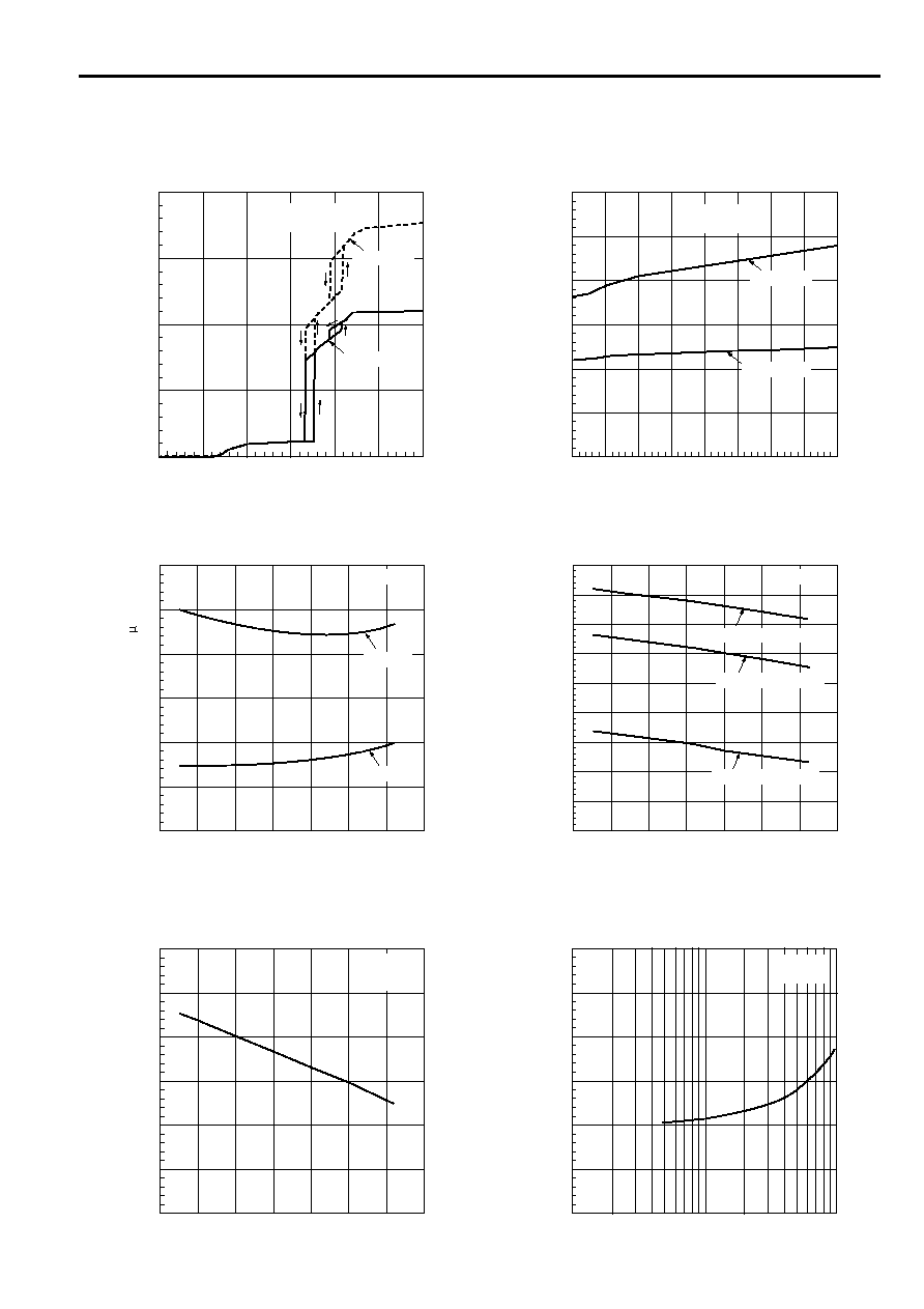
7
Operating mode supply current vs. V
CC
Operating mode supply current vs. V
CC
OFF mode supply current vs. temperature
Operating mode supply current vs. temperature
Latched mode supply current vs. temperature
Oscillation frequency vs. operating mode supply current
0
Vcc [V]
2
Oper
ating mode supply current [mA]
fosc=185kHz
fosc=1MHz
Duty=50%
IN(≠)≠FB:shorted
0.5
1
1.5
2
2.5
3
1.5
1
0.5
0
fosc=185kHz
fosc=1MHz
Duty=50%
IN(≠)≠FB:shorted
4
Vcc [V]
3
Oper
ating mode supply current [mA]
6
8
10
12
14
16
2.5
2
1.5
0
18
20
1
0.5
CS=0V
Vcc=20V
Vcc=6V
≠40
Temperature Ta [∞C]
60
≠20
0
20
40
60
80
55
50
45
40
35
30
100
OFF mode supply current [ A]
R
T
=22k
Vcc=20V (Duty=50%)
Vcc=6V (Duty=50%)
Vcc=6V (Duty=0%)
1.2
Oper
ating mode supply current [mA]
1.1
1
0.9
0.6
0.8
0.7
≠40
Temperature Ta [∞C]
≠20
0
20
40
60
80
100
1.3
1.4
1.5
Vcc=6V
R
T
=22k
CS
>
2.35V
0.85
Oper
ating mode supply current [mA]
0.8
0.75
0.7
≠40
Temperature Ta [∞C]
≠20
0
20
40
60
80
100
0.9
0.95
1
Vcc=6V
Duty=50%
1.5
Oper
ating mode supply current [mA]
1
0.5
0
Oscillation frequency [kHz]
10
100
1000
2
2.5
3
FA7700V, FA7701V
8
OUT terminal source current vs. OUT terminal voltage
OUT terminal sink current vs. OUT terminal voltage
Error amplifier gain and phase vs. frequency
0
OUT terminal voltage [V]
300
5
10
15
20
25
250
200
150
100
50
0
OUT ter
m
inal source current [mA]
350
400
450
Vcc=12V
Vcc=20V
Vcc=6V
Vcc=2.5V
0
OUT terminal voltage [V]
0.5
1
1.5
OUT ter
m
inal source current [mA]
100
50
0
150
200
1M
390
+
≠
+
0
Frequency [Hz]
1k
10k
100k
1M
10M
80
180
60
40
20
0
≠20
Gain [dB]
Gain
Phase
Phase [deg]
3
6
3
6
3
6
3
6
3
6
160
140
120
100
80
60
40
20
0
FA7700V, FA7701V
9
s
Description of each circuit
1. Reference voltage circuit
This circuit consists of the reference voltage circuit using band
gap reference, and also serves as the power supply of the
internal circuit. The precision of output is 2.23V
±
3%.
It is stabilized under the supply voltage of 2.5V or over.
The precision of reference voltage of error amplifier circuit is
0.88V
±
2%, and the reference voltage circuit is connected to the
non-inverting input of the error amplifier circuit.
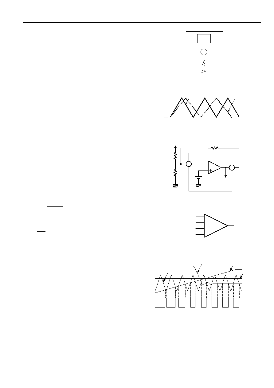
2. Oscillator
The oscillator generates a triangular waveform by charging and
discharging the built-in capacitor. A desired oscillation
frequency can be determined by the value of the resistor "R
T
"
connected to the RT terminal (Fig. 1).
The built-in capacitor voltage oscillates between approximately
0.66V and 1.1V with almost the same charging and discharging
gradients. You can set the desired oscillation frequency by
changing the gradients using the resistor connected to the RT
terminal. (Large R
T
: Low frequency, small R
T
: High frequency)
The oscillator waveform cannot be observed from the outside
because a terminal for this purpose is not provided. The
oscillator output is connected to the PWM comparator.
3. Error amplifier circuit
The IN(≠) terminal (Pin 3) is an inverting input terminal.
The non-inverting input is internally connected to the reference
voltage (0.88V
±
2%; 25∞C). The FB terminal (Pin 4) is the
output of the error amplifier. Gain setting and phase
compensation setting is done by connecting a capacitance and
a resistor between the FB terminal and the IN(≠) terminal. Vout
which is the output voltage of DC to DC converter can be
calculated by:
Gain A
V
between the Vout and the FB terminal can be
calculated by:
Vout = V
B
R1 + R2
R2
AV = ≠
R
NF
R1
Fig. 1
Fig. 2
OSC
R
T
0.66V
1.1V
RT value: small
RT value: large
≠
+
+
+
PMW output
Oscillation output
CS terminal voltage
Error amplifier output
DT voltage
V
B
R
NF
Vout
R2
R1
IN(≠)
PWM
FB
Er. AMP
3
4
(0.88V)
Fig. 3
Fig. 4
Fig. 5
PWM
output pulse
Oscillation output
Error amplifier output
CS terminal voltage
DT voltage
4. PWM comparator
The PWM comparator has 4 input terminals. (Fig. 4)
The oscillator output is compared with the CS terminal voltage ,
and the error amplifier voltage , then, the lower voltage between
and is preferred.
While the preferred voltage is lower than the oscillator output, the
PWM comparator output is Low. While the preferred voltage is higher
than the oscillator output, the PWM comparator output is High (Fig.
5). When the IC starts, the capacitor connected to the CS terminal is
charged through the resistor connected to the power supply, and
then the output pulses begin to widen gradually as the operation of
soft start.
In steady operation, the pulse width is determined based on the
voltage of the error amplifier , and then the output voltage is
stabilized. The Dead Time control voltage (
DT voltage) of FA7700
and FA7701 has different characteristics to adjust the ICs to various
types of power supply circuits being controlled and also to reduce
external discrete components as many as possible. FA7700 is
developed for fly-back circuits, and boost circuits, and the DT voltage
is set in the IC so that the maximum output duty cycle is fixed to 80%
min.. (Maximum output duty cycle changes according to operation
frequencies. ≠≠See page 6 "Maximum output duty vs. temperature".)
It prevents magnetic saturation of the transformer or the like when a
short-circuit in the output circuit occurs. FA7701 is developed for
buck circuits, and it is designed for the maximum output duty cycle of
100%. The timing chart of PWM comparator is described in Fig. 5.
FA7700V, FA7701V
10
tp [ms] Cs R
CS
1n
Vcc ≠ 1.5
Vcc ≠ 2.2
(
)
Fig. 8
0
1
2
3
4
5
6
Time
tp
Soft start
Start-up
Lower value of either 5.5V or Vcc terminal voltage
CS terminal voltage [V]
Momentary short circuit
Short circuit protection
Short circuit
2.2V
1.5V
Vcc ≠ 1.5
Rcs [M
]
Vcc ≠ 1.5
50
µ
A + I
L
1
µ
A + I
L
V
CC
V
CC
≠ 0.88
(
)
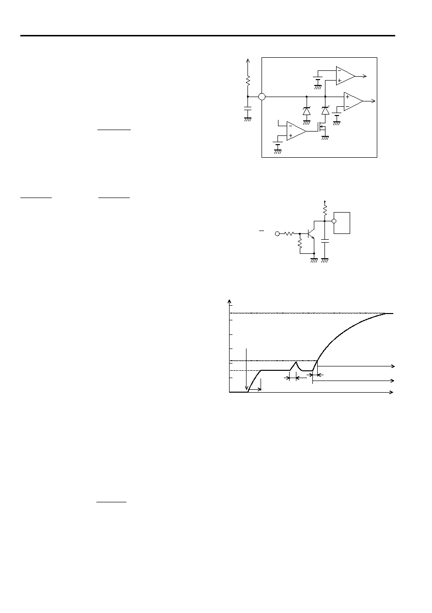
5. Soft start function
As described in Fig. 6, R
CS
is connected between CS terminal
and VCC terminal, and Cs is connected between CS terminal
and GND. The voltage of CS terminal rises when starting the
power supply, because Cs is charged by Vcc through Rcs. The
soft start function starts by charging a capacitor Cs connected
to PWM comparator. To estimate the soft start period, the time
(ts) between the start and the moment when the width of output
pulse reaches 50% is calculated by:
ts [ms] Cs R
CS
1n
Cs : Capacity of Cs [
µ
F]
Rcs : Resistance of Rcs [k
]
Vcc : Supply voltage [V]
The maximum current flowing in Rcs should be within the
recommended value (50
µ
A max.).
(I
L
: leak current of capacitor Cs)
Note: This IC operates ON/OFF function by the CS terminal (CS < 0.3V
typ. : OFF), then it turns off the internal bias voltage V
REF
(off
mode). Therefore, you can not connect the resistor "Rcs" between
CS terminal and REF terminal, and can connect the resistor only
to VCC terminal.
6. ON/OFF circuit
The ON/OFF function can be controlled by external signal to
the CS terminal, the IC becomes off mode. When the CS
terminal voltage is below 0.30V(typ.), the output of ON/OFF
comparator C3 is set to LOW, and the internal power source
V
REF
is shut off, then the IC is switched to the off mode.
The power consumption in the off mode is 40
µ
A(typ.). A
sample circuit is given in Fig. 7.
7. Timer latch short-circuit protection circuit
The short-circuit protection circuit consists of two comparators
C1, C2 (Fig. 6). In steady operation, the output of S.C.DET
comparator C2 is set to High, and the CS terminal is clamped
by the 1.5V Zener diode, because the output of error amplifier
is about 1V. If the converter output voltage drops due to a
short-circuit, when the output voltage of error amplifier rises
excesses 1.5V, the output of S.C.DET comparator C2 is set to
low, and then the clamp of Zener diode is turned off.
As a result, the voltage of CS terminal rises up to the lower
value of either 5.5 V or the voltage of VCC terminal.
If the voltage of CS terminal excesses 2.2V, the output of S.C.P
comparator C1 is set to high, and the circuit shuts down the
output circuit of the IC. When it occurs, the current
consumption of the IC is 0.9mA (typ.) because the IC is set to
OFF latch mode. The period (tp) between the occurrence of a
short-circuit in the converter output and the triggering of the
short-circuit protection function can be calculated by the
following expression:
Cs : Capacitance of Cs [
µ
F]
Rcs : Resistance of Rcs [k
]
Vcc : Supply voltage [V]
Note: When the IC is used in a product with low VCC voltage, the
period (tp) of the triggering of the short-circuit protection
described above fluctuates significantly. Therefore, sufficient
care should be taken in such cases.
Example
When Rcs=750k
, Cs=0.1
µ
F: Vcc=2.5V: tp 90ms
Vcc=3.6V: tp 30ms
Fig. 7
+
+
Output
off
FB
1.5V
2.2V
1.5V
5.5V
CS
R
CC
Cs
Rcs
S.C.P
S.C.DET
C1
C2
+
0.3 V
REF OFF
ON/OFF
C3
8
Fig. 6
CS
Cs
ON/OFF
Vcc

FA7700V, FA7701V
11
You can reset the off latch mode operation of the short-circuit
protection by either of the following ways: lowering the CS
voltage below 2.03V (typ.); lowering the Vcc voltage below the
Off threshold voltage of undervoltage lock out; 1.93V (typ.);
lowering the voltage of FB terminal below 1.5V (typ.)
The off latch mode action cannot be triggered by externally
applying voltage of over 2.2V forcibly to the CS terminal (1.5V,
ZD clamped). Characteristics of the current and the voltage of
CS terminal is shown in the characteristic curve (CS terminal
voltage vs. CS terminal sink current) on page 6. Be sure to use
the IC up to the recommended CS terminal current of 50
µ
A.
8. Output circuit
The IC contains a push-pull output stage and can directly drive
MOSFETs (FA7700: N ch, FA7701: P ch). The maximum peak
current of the output stage is a sink current of +150mA, and a
source current of ≠400mA. The IC can also drive NPN, and
PNP transistors. The maximum peak current in such cases is
±
50mA. Be sure to design the output current considering the
rating of power dissipation.
9. Power good signal circuit/ Undervoltage lockout circuit
The IC contains a protection circuit against undervoltage
malfunctions to protect the circuit from the damage caused by
malfunctions when the supply voltage drops. When the supply
voltage rises from 0V, the circuit starts to operate at VCC of
2.07V (typ.) and outputs generate pulses. If a drop of the
supply voltage occurs, it stops output at VCC of 1.93V (typ.).
when it occurs, the CS terminal is turned to Low level and then
it is reset. The power good signal circuit monitors the voltage of
REF terminal, and stops output until the voltage of REF
terminal excesses approximately 2V to prevent malfunctions.
s
Design advice
1. Setting the oscillation frequency
As described in item 2 "Oscillator" of "Description of each
circuit", a desired oscillation frequency can be determined by
the value of the resistor connected to the RT terminal. When
designing an oscillation frequency, you can set any frequency
between 50kHz and 1MHz. You can roughly obtain the
oscillation frequency from the characteristic curve "Oscillation
frequency (fosc) vs. timing resistor resistance(R
T
)" or the value
can be calculated by the following expression.
f
OSC
: Oscillation frequency [kHz]
R
T
:
Timing resistor [k
]
This expression, however, can be used for rough calculation,
the value obtained is not guaranteed. The operation frequency
varies due to the conditions such as tolerance of the
characteristics of the ICs, influence of noises, or external
discrete components. When determining the values, be sure to
verify the effectiveness of the values of the components in an
actual circuit.
2. Operation around the maximum or the minimum output
duties
As described in characteristic curves on page 5, "output duty
cycle vs. FB terminal voltage (V
FB
)" and "output duty cycle vs.
CS terminal voltage (Vcs)", the linearity of the output duty of
this IC drops around the minimum output duty and the
maximum output duty (FA7701 only). This phenomena are
conspicuous when operating in a high frequency (when the
pulse width is narrow). Therefore be careful when using high
frequency.
3. Restriction of external discrete components
To achieve a stable operation of the ICs, the value of external
discrete components connected to Vcc, R
EF
, CS, FB terminals
should be within the recommended operational conditions.
4. Loss calculation
Since it is difficult to measure IC loss directly, the calculation to
obtain the approximate loss of the IC connected directly to a
MOSFET is described below.
When the supply voltage is Vcc, the current consumption of the
IC is Icc, the total input gate charge of the driven MOSFET is
Qg, the switching frequency is fsw, the total loss Pd of the IC
can be calculated by:
Pd Vcc (Icc + Qg fsw).
The values in this expression is influenced by the effects of the
dependency of supply voltage, the characteristics of
temperature, or tolerance. Therefore, be sure to verify
appropriateness of the value considering the factors above
under all applicable conditions.
Example:
When V
CC
= 6V, in the case of a typical IC, from the
characteristic curve, Icc=1.2mA. When operating in Qg = 6nC,
fsw = 500kHz, Pd should be:
Pd 6 (1.2mA + 6nC 500kHz) 25.2mW
f
OSC
= 3000 R
T
≠0.9
R
T
=
3000
1.11
f
OSC
(
)
FA7700V, FA7701V
12
s
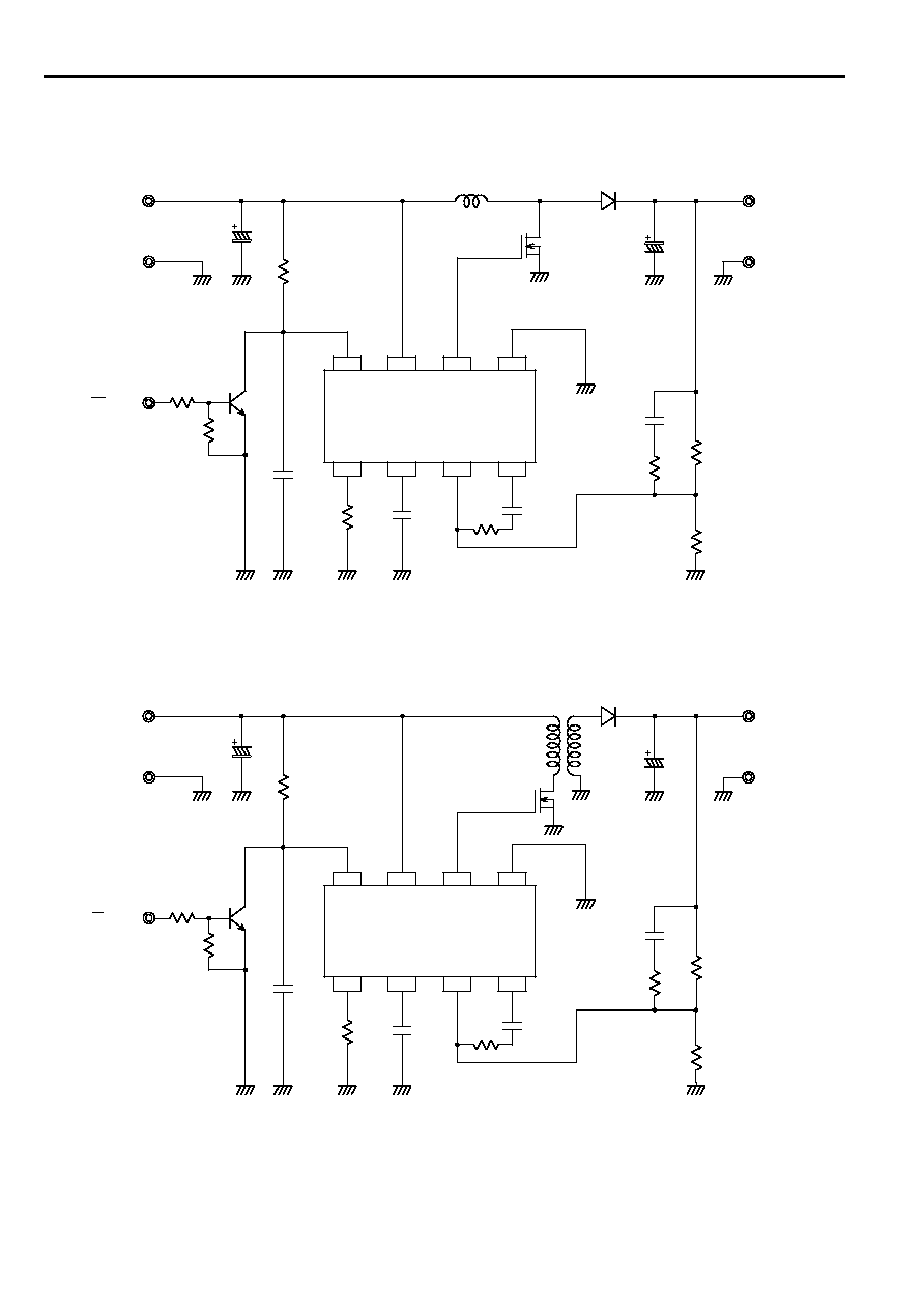
Application circuit
FA7700
ON /OFF
FA7700
RT
REF
IN-
FB
1
2
3
4
8
7
6
5
GND
OUT
VCC
CS
Vout
12V/0.2A
Vin
2.5~11V
ON /OFF
FA7700
RT
REF
IN-
FB
1
2
3
4
8
7
6
5
GND
OUT
VCC
CS
Vout
Vin
FA7700V, FA7701V
13
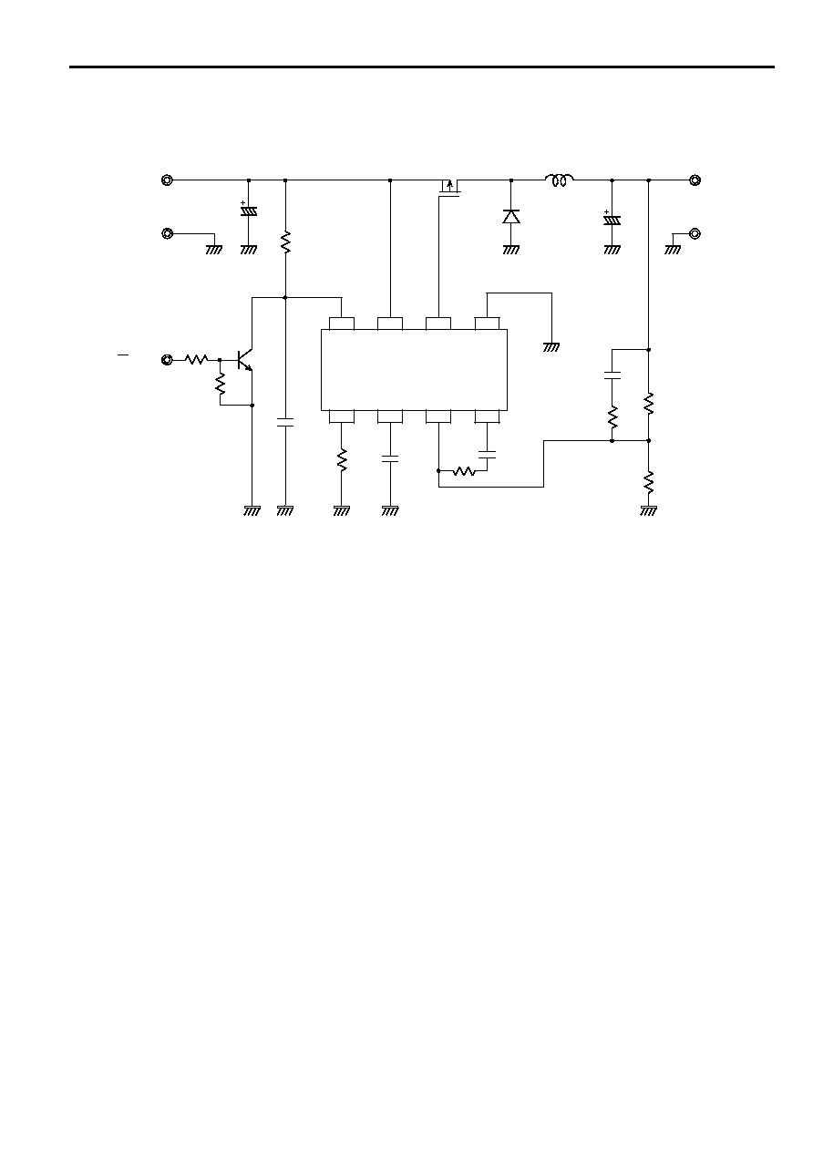
s
Application circuit
FA7701
Parts tolerances characteristics are not defined in the circuit design
sample shown above. When designing an actual circuit for a
product, you must determine parts tolerances and characteristics for
safe and economical operation.
FA7701
RT
REF
IN-
FB
1
2
3
4
8
7
6
5
GND
OUT
VCC
CS
ON /OFF
Vin
7~18V
Vout
5V/0.5A