 | –≠–ª–µ–∫—Ç—Ä–æ–Ω–Ω—ã–π –∫–æ–º–ø–æ–Ω–µ–Ω—Ç: FA7704M | –°–∫–∞—á–∞—Ç—å:  PDF PDF  ZIP ZIP |

1
Quality is our message
Quality is our message
Quality is our message
Quality is our message
FA7703/04
FUJI Power Supply Control IC
FA7703/04
Application Note
June -2002
Fuji Electric Co., Ltd.
Matsumoto Factory

2
Quality is our message
Quality is our message
Quality is our message
Quality is our message
FA7703/04
1.This Data Book contains the product specifications, characteristics, data, materials, and structures as of
June 2002. The contents are subject to change without notice for specification changes or other
reasons. When using a product listed in this Data Book, be sure to obtain the latest specifications.
2. All applications described in this Data Book exemplify the use of Fuji's products for your reference only.
No right or license, either express or implied, under any patent, copyright, trade secret or other
intellectual property right owned by Fuji Electric Co., Ltd. is (or shall be deemed) granted. Fuji makes
no representation or warranty, whether express or implied, relating to the infringement or alleged
infringement of other's intellectual property rights, which may arise from the use of the applications,
described herein.
3. Although Fuji Electric is enhancing product quality and reliability, a small percentage of semiconductor
products may become faulty. When using Fuji Electric semiconductor products in your equipment, you
are requested to take adequate safety measures to prevent the equipment from causing a physical
injury, fire, or other problem if any of the products become faulty. It is recommended to make your
design fail-safe, flame retardant, and free of malfunction.
4.The products introduced in this Data Book are intended for use in the following electronic and electrical
equipment, which has normal reliability requirements.
∑ Computers ∑ OA equipment ∑ Communications equipment (terminal devices)
∑ Measurement equipment ∑ Machine tools ∑ Audiovisual equipment ∑ Electrical home appliances
∑ Personal equipment ∑ Industrial robots etc.
5.If you need to use a product in this Data Book for equipment requiring higher reliability than normal,
such as for the equipment listed below, it is imperative to contact Fuji Electric to obtain prior approval.
When using these products for such equipment, take adequate measures such as a backup system to
prevent the equipment from malfunctioning even if a Fuji's product incorporated in the equipment
becomes faulty.
∑ Transportation equipment (mounted on cars and ships) ∑ Trunk communications
equipment
∑ Traffic-signal control equipment ∑ Gas leakage detectors with an auto-shut-off feature
∑ Emergency equipment for responding to disasters and anti-burglary devices ∑ Safety devices
6. Do not use products in this Data Book for the equipment requiring strict reliability such as (without
limitation)
∑ Space equipment ∑ Aeronautic equipment ∑ Atomic control equipment
∑ Submarine repeater equipment ∑ Medical equipment
7. Copyright © 1995 by Fuji Electric Co., Ltd. All rights reserved. No part of this Data Book may be
reproduced in any form or by any means without the express permission of Fuji Electric.
8. If you have any question about any portion in this Data Book, ask Fuji Electric or its sales agents
before using the product. Neither Fuji nor its agents shall be liable for any injury caused by any use of
the products not in accordance with instructions set forth herein.
WARNING

3
Quality is our message
Quality is our message
Quality is our message
Quality is our message
FA7703/04
CONTENTS
Page
1. Description ......................................................... 4
2. Features ............................................................. 4
3. Outline ................................................................ 4
4. Block diagram ..................................................... 5
5. Selection Guide.................................................... 5
6. Pin assignment ................................................... 5
7. Ratings and characteristics ................................ 6
8. Characteristics curves.......................................... 9
9. Description of each circuit .................................. 13
10. Design advice ..................................................... 16
11. Application circuit ............................................... 21
Note
∑ Parts tolerance and characteristics are not defined in all application described in this Data book. When
design an actual circuit for a product, you must determine parts tolerances and characteristics for safe and
stable operation.

4
Quality is our message
Quality is our message
Quality is our message
Quality is our message
FA7703/04
Description
FA7703/04 are the PWM type DC-DC converter control ICs with 2ch output that can directly drive power
MOSFETs. FA7703/04 feature CMOS devices with high breakdown voltage and also low power
consumption are achieved. By means of their small and thin package (1.1mm max.), and high frequency
operation (to 1MHz), FA7703/04 are completely suitable for the use of very small DC-DC converters.
Besides, you can select a Pch or Nch type of MOSFET directly driven by FA7703/04, and also you can
practically design any kind of DC-DC converter circuit like a boost converter, a buck converter, a inverting
converter, a fly-back converter, and so on.
1. Features
Wide range of supply voltage: VCC=2.5 to 20V
Direct driving of MOSFET
Switching Pch/Nch driving is available (channel 1 only)
Low current consumption is achieved by CMOS process:
1.8mA (typ.) in operation
2ch PWM control IC
High frequency operation is available: 50kHz to 1MHz
Simple setting of operation frequency with a timing resistor
Soft start setting is available
Setting of the limitation of maximum output duty cycle is available in each channel
Built-in protection function for undervoltage lockout
Highly accurate reference voltage:
VREF: 1.00V
±
1%, VB: 1.00V
±
2%, VREG: 2.20V
±
2%
Built-in output timer latched short-circuit protection circuit
Thin and small package: TSSOP-16, SOP-16
2. Outline
TSSOP-16 (V) SOP-16 (M)
0.
7
1
±
0
.
1
5.
3
±
0
.
3
0.4 ±0.05
1.27
7.
8
±
0
.
2
1.
9
±
0.
2
10.2 ±0.3
4.
4
0
±
0
.
0
5
0.65
6.
4
±
0
.
1
5.0 ±0.1
1.
10
M
A
X
units:mm

5
Quality is our message
Quality is our message
Quality is our message
Quality is our message
FA7703/04
3.Block diagram
4. Selection Gide
Ch.1(OUT1)
Buck, Boost, Fly-back
FA7703
Ch.2(OUT2)
Buck, Inverting (Pch driven)
Ch.1(OUT1)
Buck, Boost, Fly-back
FA7704
Ch.2(OUT2)
Boost, Fly-back (Nch driven)
5. Pin assignment
Pin No
Pin
symbol
Description
1
RT
Oscillator timing resistor
2
CS
Soft start, Timer latched short circuit protection, ON/OFF control
3 DT2
Ch.2
Dead Time Adjustment
4
IN2+
Ch.2 non-inverting input to error amplifier
5
IN2-
Ch.2 inverting input to error amplifier
6
FB2
Ch.2 output o error amplifier
7 GND
Ground
8 OUT2
Ch.2
output
9 VCC
Power
supply
10 OUT1
Ch.1
output
11
SEL
Selection of type of driven MOSFET (OUT1)
12
FB1
Ch.1 output o error amplifier
13
IN1-
Ch.1 inverting input to error amplifier
14 REF
Reference
voltage
15 DT1
Ch.1
Dead Time Adjustment
16 REG
Regulated
voltage
output
16
15
14
13
12
11
10
9
1
2
3
4
5
6
7
8
REG
DT1
REF
IN1-
FB1
SEL1
OUT1
VCC
RT
CS
DT2
IN2+
IN2-
FB2
GND
OUT2
+
-
+
+
+
-
+
+
OSC
Power G ood Signal
Reference
voltage
+
-
-
UVLO
BIAS
1V
Er.Am p1
Er.Am p2
PW M.Com p1
PW M.Com p2
1.5V
2.0V
1.3V
S.C.DET
S.C.P
O N/O FF
O N/O FF
BIAS
2.2V
I
CS
FA7704

6
Quality is our message
Quality is our message
Quality is our message
Quality is our message
FA7703/04
6.Ratings and characteristics
The contents are subject to change without notice. When using a product, be sure to obtain the latest
specifications.
(1)Absolute maximum ratings
Item Symbol
Ratings
Units
Power supply voltage
V
CC
20 V
REF Terminal output current
I
REF
1 mA
REG Terminal output current
I
REG
2 mA
I
SOpeak
-400(peak) mA
OUT1, OUT2 Terminal source current
I
SOcont
-50(continuos) mA
I
SIpeak
+150(peak) mA
OUT1, OUT2 Terminal sink current
I
SIcont
+50(continuos) mA
RT,CS,REG,REF,IN1-,IN2+,IN2-,FB1,
FB2,DT1,DT2,SEL1 Terminal voltage
V
LOGIC
+2.5(max.)
-0.3(min.)
V
TSSOP 300
Power dissipation
(Ta25
∞
C)*
SOP
P
d
400
mW
Operating ambient temperature
T
a
-30 to +85
∞C
Operating junction temperature
T
j
+125 ∞C
Storage temperature
T
stg
-40 to +150
∞C
*:Maximum dissipation curve at Ta25
∞
C is shown under figure.
(2)Recommended operating conditions
Item Symbol
MIN.
TYP.
MAX.
Units
Supply voltage
V
cc
2.5 6 18 V
DC feedback resistor of
error amplifier
R
NF
100
k
VCC terminal capacitance*
C
VCC
0.1
µ
F
REG terminal capacitance
C
REG
0.047 0.1
1
µ
F
CS terminal capacitance
C
CS
0.01
10
µ
F
Oscillation frequency
f
OSC
50 1000 kHz
Pch,PNP driving
V
SEL1L
Connect
to
GND
SEL1 terminal
voltage
Nch,NPN driving
V
SEL1H
Connect to REG terminal
*Please select the proper value by input-output conditions of power supply.
Maximum power dissipation curve
0
100
200
300
400
500
-30
0
30
60
90
120
150
Ambient temperature Ta[∞C]
Maximum power dissipation Pd[mW]
TSSO
SOP

7
Quality is our message
Quality is our message
Quality is our message
Quality is our message
FA7703/04
(3)Electrical characteristics
[Unless otherwise standard,Ta=25
∞
C,Vcc=6V,R
T
=22k
]
(1) Internal Bias Section (REF terminal voltage)
Item Symbol Conditions MIN.
TYP.
MAX.
Units
Output Voltage
V
REF
REF terminal load current
I
REF
=0mA
0.990 1.000 1.010 V
Line Regulation
V
LINEF
Vcc=2.5
to
18V,I
REF
=0mA
±1
±5
mV
Load Regulation
V
LDF
IREF=0
to
1mA
-10
-3
mV
Variation
with temperature
V
TCF
Ta=-30 to +85
∞
C
Change rate for value at 25
∞
C
-0.8 to
+0.2
%
(2) Regulated Voltage for Internal Control Blocks Section (REG terminal voltage)
Item Symbol Conditions MIN.
TYP.
MAX.
Units
Output Voltage
V
REG
REG terminal load current
I
REG
=0mA
2.156 2.200 2.244 V
Line Regulation
V
LINEG
Vcc=2.5
to
18V,I
REG
=0mA
±4
±14
mV
Load Regulation
V
LDG
I
REG
=0 to 2mA
-12
-2
mV
Variation
with temperature
V
TCG
Ta=-30 to +85
∞
C
Change rate for value at 25
∞
C
-0.8 to
+0.2
%
(3) Oscillator Section
Item Symbol Conditions MIN.
TYP.
MAX.
Units
Oscillation frequency
f
OSC
R
T
=22k
160 190 220 kHz
Line Regulation
f
LINE
Vcc=2.5
to
18V
±0.1
%
f
TC1
Ta=+25 to -30
∞
C
, f=50k to 1MHz
±2 %
Variation
With temperature
f
TC2
Ta=+25 to +85
∞
C
, f=50k to1MHz
±3 %
(4) Error Amplifier Section (Input:IN1-,IN2+,IN2-,Output:FB1,FB2 terminal)
Item Symbol Conditions MIN.
TYP.
MAX.
Units
Reference Voltage
(ch1)
V
B
IN1- terminal threshold voltage
0.980
1.000
1.020
V
Input offset (ch2)
V
OFST
(IN2+) - (IN2-)
-
-
±10
mV
Common mode input
voltage
V
IN
0.3 1.4 V
Input Current
I
IN
-100 0 +100 nA
Open Loop Gain
A
VO
70
dB
Unity Gain Bandwidth
f
T
1.5 MHz
Output Source Current
I
OHE
FB1,2
terminal voltage=V
REF
-0.5V
-220 -160 -100
µ
A
Output sink Current
I
OLE
FB1,2
terminal
voltage=0.5V
3
6
12 mA
(5) Pulse Width Modulation Section (FB1,FB2 terminal)
Item Symbol Conditions MIN.
TYP.
MAX.
Units
Input threshold voltage
V
FB0
Duty
Cycle=0%
0.550 0.650 0.750 V
Input threshold voltage
V
FB100
Duty
Cycle=100%
1.000 1.100 1.200
V
(6) Dead Time Adjustment Circuit Section (DT1, DT2 terminal)
Item Symbol Conditions MIN.
TYP.
MAX.
Units
Input threshold voltage
V
DT0
Duty
Cycle=0%
0.550 0.650 0.750 V
Input threshold voltage
V
DT100
Duty
Cycle=100%
1.000 1.100 1.200
V

8
Quality is our message
Quality is our message
Quality is our message
Quality is our message
FA7703/04
(7) Under Voltage Lock-Out Section (VCC terminal)
Item Symbol Conditions MIN.
TYP.
MAX.
Units
ON threshold
V
CCON
2.00 2.25
V
OFF threshold
V
CCOF
1.40 1.85
V
Hysteresis Voltage
V
CCHY
0.05 0.15 0.35
V
Ta=-30 to +25
∞
C
+0.3 mV/∞C
Variation
with temperature
V
CCHY
Ta=+25to +85
∞
C
-0.1
mV/
∞
C
(8) Soft Start Section (CS terminal)
Item Symbol Conditions MIN.
TYP.
MAX.
Units
Output source current
I
CS
CS=0V -2.8
-2.2
-1.6
µ
A
Threshold Voltage1
V
CS0
Duty
Cycle=0%
0.550 0.650 0.750 V
Threshold Voltage2
V
CS50
Duty
Cycle=50%
0.880
V
(9) Short circuit Protection Section (FB terminal, CS terminal)
Item Symbol Conditions MIN.
TYP.
MAX.
Units
Short Detection
Threshold Voltage
V
FBTH
FB terminal voltage
1.350
1.500
1.650
V
Latched Mode
Threshold Voltage
V
CSTH
CS terminal voltage
1.900
2.000
2.100
V
Latched Mode
Reset Voltage
V
CSRE
CS terminal voltage
1.830
V
Latched Mode
Hysteresis
V
CSHY
CS terminal voltage
30
170
300
mV
V
CSCL1
FB terminal voltage<1.35V
1.200
1.270
1.340
V
CS terminal
Clamped Voltage
V
CSCL2
FB terminal voltage>1.65V
2.120
2.200
2.280
V
(10) Output Stage Section (OUT1,OUT2 terminal,SEL1 terminal)
Item Symbol Conditions MIN.
TYP.
MAX.
Units
High side on resistance
R
ONH
V
CC
=6V,Source Current=-50mA
10
20
High side on resistance
R
ONH
V
CC
=2.5V,Source
Current=-50mA
18 36
Low side on resistance
R
ONL
V
CC
=6V,Sink Current=+50mA
5
10
Low side on resistance
R
ONL
V
CC
=2.5V,Sink
Current=+50mA 5 10
trn
330pF Load to GND terminal
20
ns
Rise Time
trp
330pF Load to VCC terminal
20
ns
tfn
330pF Load to GND terminal
35
ns
Fall Time
tfp
330pF Load to VCC terminal
35
ns
V
SEL1L
Pch-MOSFET,
PNP transistor driving
0 0.2
V
SEL1 terminal Input
Voltage
V
SEL1H
Nch-MOSFET,
NPN transistor driving
V
REG
-
0.2
V
REG
V
(11) Overall Section (VCC terminal)
Item Symbol Conditions MIN.
TYP.
MAX.
Units
I
CC0
Duty Cycle=0%,OUT1/2:open
CS=0V, FB1,FB2
V
REG
R
T
=22k
,f
190kHz
1.3
1.9
mA
I
CC1
Duty Cycle=80%,OUT1/2:open
R
T
=22k
,f
190kHz
1.8
2.7
mA
Operating mode
Supply Current
I
CC2
Duty Cycle=80%,OUT1/2:open
R
T
=3k
,f
1MHz
3.1
4.7
mA
Latched mode
Supply Current
I
CCLAT
CS>2.1V,FB1,FB2
V
REG
,
R
T
=22k
,f
190kHz
1.3
1.9
mA
9
Quality is our message
Quality is our message
Quality is our message
Quality is our message
FA7703/04
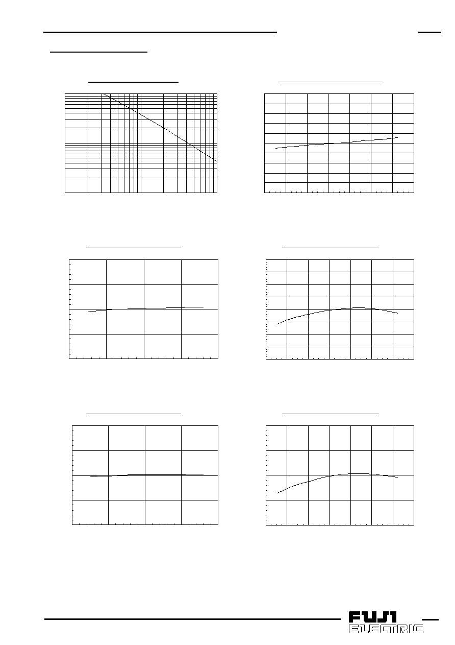
7. Characteristics curves
Timing resistor vs.Oscillation frequency
10
100
1000
1
10
100
Timing resistor RT[k
]
Oscillation frequency [kHz]
Vcc=6V
Regulated voltage vs.Supply voltage VCC
2.18
2.19
2.20
2.21
2.22
0
5
10
15
20
Supply voltage Vcc[V]
Regulated voltage VREG[V
]
IREG=0A,RT=22k
Reference voltage vs.Supply voltage VCC
0.990
0.995
1.000
1.005
1.010
0
5
10
15
20
Supply voltage Vcc[V]
Reference voltage VREF[V
]
IREF=0A,RT=22k
Oscillation frequency vs.ambient temperature
185
186
187
188
189
190
191
192
193
194
195
-40
-20
0
20
40
60
80
100
Ambient temperature Ta[∞C]
Oscillation frequency [kHz]
Vcc=6V,RT=22k
Regulated voltage vs.Ambient temperature
2.16
2.17
2.18
2.19
2.20
2.21
2.22
2.23
2.24
-40
-20
0
20
40
60
80
100
Ambient temperature Ta[∞C]
Regulated voltage VREG[V
]
IREG=0A,RT=22k
Reference voltage vs.Ambient temperature
0.98
0.99
1.00
1.01
1.02
-40
-20
0
20
40
60
80
100
Ambient temperature Ta[∞C]
Reference voltage VREF[V
]
IREF=0A,RT=22k

10
Quality is our message
Quality is our message
Quality is our message
Quality is our message
FA7703/04
FB terminal voltage vs.Duty cycle
0
10
20
30
40
50
60
70
80
90
100
0.5
0.6
0.7
0.8
0.9
1.0
1.1
1.2
FB terminal voltage [V]
Duty cycle [%]
FA7703/04:OUT1 Nch driven (SEL1=REG)
FA7704:OUT2
fosc=1MHz
fosc=190kHz
DT terminal voltage vs.Duty cycle
0
10
20
30
40
50
60
70
80
90
100
0.5
0.6
0.7
0.8
0.9
1.0
1.1
1.2
DT terminal voltage [V]
Duty cycle [%]
fosc=1MHz
fosc=190kHz
FA7703/04:OUT1 Nch driven (SEL1=REG)
FA7704:OUT2
CS terminal voltage vs.Duty cycle
0
10
20
30
40
50
60
70
80
90
100
0.5
0.6
0.7
0.8
0.9
1.0
1.1
1.2
CS terminal voltage [V]
Duty cycle [%]
fosc=1MHz
fosc=190kHz
FA7703/04:OUT1 Nch driven (SEL1=REG)
FA7704:OUT2
FB terminal voltage vs.Duty cycle
0
10
20
30
40
50
60
70
80
90
100
0.5
0.6
0.7
0.8
0.9
1.0
1.1
1.2
FB terminal voltage [V]
Duty cycle [%]
fosc=1MHz
fosc=190kHz
FA7703/04:OUT1 Pch driven (SEL1=GND)
FA7703:OUT2
DT terminal voltage vs.Duty cycle
0
10
20
30
40
50
60
70
80
90
100
0.5
0.6
0.7
0.8
0.9
1.0
1.1
1.2
DT terminal voltage [V]
Duty cycle [%]
fosc=1MHz
fosc=190kHz
FA7703/04:OUT1 Pch driven (SEL1=GND)
FA7703:OUT2
CS terminal voltage vs.Duty cycle
0
10
20
30
40
50
60
70
80
90
100
0.5
0.6
0.7
0.8
0.9
1.0
1.1
1.2
CS terminal voltage [V]
Duty cycle [%]
fosc=1MHz
fosc=190kHz
FA7703/04:OUT1 Pch drivenb (SEL1=GND)
FA7703:OUT2

11
Quality is our message
Quality is our message
Quality is our message
Quality is our message
FA7703/04
Duty cycle vs. Ambient temperature
78
80
82
84
86
88
90
92
94
-40
-20
0
20
40
60
80
100
Ambient temperature Ta[∞C]
duty cycle [%]
DT terminal voltage
1.05V
fosc=190kHz
fosc=1MHz
FA7703/04:OUT1 Nch drive (SEL1=REG)
FA7704:OUT2
Operating mode supply current vs.Supply voltage
0.0
0.5
1.0
1.5
2.0
2.5
3.0
0.0
0.5
1.0
1.5
2.0
2.5
3.0
3.5
Supply voltage Vcc[V]
Operating mode supply current [mA
]
Duty=80%,
IN(-)-FB:shorted
fosc=190kHz
fosc=1MHz
Operating supply current vs.Ambient temperature
1.0
1.5
2.0
2.5
-40
-20
0
20
40
60
80
100
Ambient temperature Ta[∞C]
Operating supply current [mA]
Duty=80%
RT=22k
Vcc=6V
Duty cycle vs. Ambient temperature
78
80
82
84
86
88
90
92
94
-40
-20
0
20
40
60
80
100
Ambient temperature Ta[∞C]
duty cycle [%]
DT terminal voltage
1.05V
fosc=190kHz
fosc=1MHz
FA7703/04:OUT1 Pch drive (SEL1=GND)
FA7703:OUT2
CS terminal voltage vs.Ambient temperature
1.21
1.23
1.25
1.27
1.29
1.31
1.33
-40
-20
0
20
40
60
80
100
Ambient temperature Ta[∞C]
CS terminal voltage [V
]
FB1,FB2<1.35V

12
Quality is our message
Quality is our message
Quality is our message
Quality is our message
FA7703/04
OUT terminal High side voltage vs.
Source current
0
50
100
150
200
250
300
350
400
450
0
5
10
15
20
25
OUT terminal voltage [V]
OUT terminal source urrent [mA
]
OUT1/2
Vcc=20V
Vcc=2.5V
Vcc=4.5V
Vcc=6.0V
Error Amplifier gain and Phase vs.frequency
-20
-10
0
10
20
30
40
50
60
70
80
Frequency [Hz]
GAIN [dB]
-20
0
20
40
60
80
100
120
140
160
180
PHASE [deg]
GAIN
PHASE
1
1k
10k
100k
1M
10M
10
OUT terminal Low side voltage vs.Sink current
0
20
40
60
80
100
120
140
160
180
200
0.0
0.5
1.0
1.5
2.0
2.5
OUT terminal voltage [V]
OUT terminal sink current [mA
]
OUT1/2
CS terminal source current vs.Ambient temperature
-2.40
-2.35
-2.30
-2.25
-2.20
-2.15
-2.10
-2.05
-2.00
-40
-20
0
20
40
60
80
100
Ambient temperature Ta[∞C]
CS terminal source current [
A]
1M
390

13
Quality is our message
Quality is our message
Quality is our message
Quality is our message
FA7703/04
8. Description of each circuit
(1)Reference Voltage Circuit
The reference voltage circuit of FA7703/04
generates the reference voltage (VREF) of
1.00V±1% compensated in temperature from
VCC voltage, and the regulated voltage (VREG)
of 2.2V ±2% for internal controlling. These
voltages start to output when the undervoltage
lockout protection (UVLO) is cancelled, and
they stabilize after the supply voltage (VCC)
reaches up to approx. 2.4V or higher. The
reference voltage (VREF) is connected to the
non-inverting input of Error Amplifier 1 and
serves as the reference voltage of Error
Amplifier 1. Because of Error Amplifiers have
offset voltage then, the precision of voltage in
practical use is 1.00V±2%. The voltage (VREF)
outputs externally from REF terminal, therefore,
it can serve as a stabilized power source. When
using it, be sure to set the output current 1mA
or below.
The regulated voltage (VREG) for internal
controlling serves as the stabilized power
source for maximum output duty setting or the
like. Be sure to set the output current 2mA or
below in operation in this case. This voltage
also serves as the control power source of all
the internal circuits of FA7703/04. A capacitor
for stabilization (CREG) is needed to be
connected to the VREG terminal. See
recommended operating conditions to
determine capacitance.
(2)Oscillator
The oscillator of FA7703/04 generates
triangular waveforms by charging and
discharging the built-in capacitor. Any desired
oscillation frequency can be obtained by setting
the value of the resistor connected to RT
terminal (Fig. 1).
The voltage oscillates between approximately
0.65V and 1.10V in charging and discharging
with almost the same gradients (Fig. 2). Your
desired oscillation frequency can be determined
by changing the gradient using the resistor (RT)
connected to RT terminal. (Large RT: Low
frequency, small RT: High frequency) The
waveforms of oscillator cannot be observed from
the outside because a terminal for this purpose
is not provided.
Approximately DC 1V is output to RT terminal.
The oscillator output is connected to PWM
comparator.
(3)Error Amplifier Circuit
Error Amplifier 1 of FA7703/04 has the inverting
input IN1(-) terminal (Pin13). The non-Inverting
input is internally connected to the reference
voltage (VB) of 1.00V±2% at 25∞C. Because
error Amplifier 2 of FA7703/04 has the inverting
input IN2(-) terminal (Pin5) and non-inverted
input IN2(+) terminal (Pin4) outputting externally,
various circuit can be designed by kinds of
external circuit structures. FB terminals (Pin6,
Pin12) are the outputs of Error Amplifiers.
Voltage Gain and phase compensation can be
set by connecting a capacitor (C) and a resistor
(R) between FB terminal and IN(-) terminal.(Fig.
3) For more information about the connection for
each output voltage of power supply, refer to
Design Advice.
Fig.2
R
T
value: large
R
T
value: small
0.65V
1.10V
Fig.3
12
13
4
5
6
14
Com p
Com p
V
B
(1.0V)
Er.Am p.1
Er.Am p.2
IN1-
REF
FB1
FB2
IN2-
IN2+
Vout1
Vout2
R
NF
1
R
NF2
R1
R2
R3
R4
1
OSC
RT
R
T
Fig.1

14
Quality is our message
Quality is our message
Quality is our message
Quality is our message
FA7703/04
(4)PWM comparator
PWM comparator of FA7703/04 has 4 input
terminals. (Fig. 4) The oscillator output
2
is
compared with the CS terminal voltage
1
, the
DT terminal voltage
3
, and the Error Amplifier
output
4
. Among those 3 inputs of
1
,
3
, and
4
, the one with the lowest voltage is chosen and
given priority. While the value of the chosen
voltage is lower than the value of the waveform
of oscillator output, PWM comparator output is
set to LOW. Similarly, while the value of the
chosen voltage is higher than the waveform of
oscillator output, PWM comparator output is set
to HIGH. (Fig. 5)
When FA7703/04 are turning ON, the soft start
function starts according to the CS terminal
voltage
1
, then the output pulses begin to widen
gradually. The maximum pulse width is adjusted
by changing the DT terminal voltage. In steady
operation, the pulse width is determined with the
condition of the Error Amplifier output
4
, and
then the output voltage of DC-DC converter is
stabilized. The operation flow chart of PWM
comparator and OUT terminal is shown in Fig. 5.
The output polarity of OUT1 terminal changes
according to the condition of SEL1 terminal. The
polarity of OUT 2 terminal is different between
FA7703 and FA7704; accordingly, select the type
for your desired circuit design.
(5)Soft start function
As described in Fig. 6, a capacitor C
CS
is
connected to CS terminal. When the power
supply of FA7703/04 starts and the undervoltage
lockout protection circuit (UVLO) is cancelled,
the capacitor C
CS
is charged by the internal
current source (2.2
µ
A. typ.), and the voltage of
CS terminal rises gradually. Since the voltage of
CS terminal is connected to PWM comparator,
the output pulses begin to widen gradually, and
then the soft start function starts as a result. (Fig.
5)
(6)Timer latch short-circuit protection circuit
The short-circuit protection circuit of FA7703/04
consists of two comparators. (S.C. DET
comparator, S.C.P comparator) In steady
operation, the output of Error Amplifier is
approximately 1V, accordingly, the output of
S.C.DET comparator is set to High, and the
voltage of CS terminal is clamped at 1.27V. If the
output voltage drops due to a short-circuit or the
like, the output voltage of Error Amplifiers rises.
When the output voltage of Error Amplifiers
exceeds 1.5V(typ.), the output of S.C.DET
comparator is set to Low, and the clamp action
at the CS terminal voltage of 1.27V is cancelled,
then the voltage of CS terminal rises up to the
VREG voltage. When the voltage of CS terminal
exceeds 2.0V(typ.), the output of S.C.P
comparator is set to High, accordingly, the
output of FA7703/04 is shut off. In this case,
FA7703/04 operate in OFF latch mode and the
current consumption in this mode is 1.3mA(typ.).
The operating waveform of the voltage of CS
terminal is shown in Fig. 7.
The approximate time (tp) between the
occurrence of a short-circuit in the output and
the triggering of the short-circuit protection
+
-
+
+
Oscillation voltage
CS term inal voltage
DT term inal voltage
Error Am plifier output
PW M output
1
2
3
4
Fig.4
+
-
-
1.5V
2.0V
1.27V
S .C .D E T
S .C .P
FB
U V LO
output off
2
2.2
µ
A
C
CS
C S
V C C
Fig.6
Fig.5
PW M
output
O UT1
Nch driv en
(SEL1:REG )
O UT1
Pch driv en
(SEL1:G ND)
O UT2
FA7703
O UT2
FA7704
Oscillation voltage
CS term inal voltage
DT term inal voltage
Error Am plifier output
4
3
1
2

15
Quality is our message
Quality is our message
Quality is our message
Quality is our message
FA7703/04
function can be calculated with
CS
CS
I
C
0.7
tp[s]
◊
where, C
CS
: Capacitance of CS terminal [
µ
F]
I
CS
: Output source current of CS terminal [
µ
A]
(2.
2µ
, typ.)
You can reset the timer latch action for the
short-circuit protection function by changing the
voltage of either VCC terminal or CS terminal to
the following values.
VCC terminal: below UVLO voltage (1.85V typ.)
CS terminal: below 1.83V(typ.)
(7)Output circuit
FA7703/04 contain a push-pull output stage
and can directly drive MOSFETs. The peak
current of OUT terminal is the maximum sink
current of +150mA, and the source current of
-400mA. FA7703/04 can also drive both NPN
and PNP type transistors. And in such cases,
the maximum continuous current is ±50mA.
When designing the value of output current, be
sure to consider the allowable loss accordingly.
(See Design advice)
Ch1 of FA7703/04 is available for driving both
types of MOSFETs and you can determine the
type of MOSFET, which is connected externally
by selecting the connection of SEL1 terminal
(Pin11). If SEL terminal is connected to GND
terminal, FA7703/04 can drive a Pch MOSFET. If
SEL terminal is connected to REG terminal, they
can drive Nch MOSFET.
You can accordingly design a buck converter
circuit by Pch MOSFET driving, and a boost
circuit or a fly-back converter circuit by Nch
MOSFET driving.
DO NOT leave SEL1 terminal open in operation,
and be sure to connect it to either GND terminal
or REG terminal.
(8)Power good signal/Undervoltage lockout
protection circuit (UVLO)
To protect FA7703/04 from malfunction when
the supply voltage drops, there is built-in
undervoltage lockout as a protection circuit.
When the supply voltage rises from 0V, the
UVLO circuit is canceled at VCC of 2.0V(typ.).
When the supply voltage drops, the UVLO circuit
shuts off the output at VCC of 1.85V(typ.). In this
case, CS terminal is reset to Low level.
Power good signal circuit monitors the voltage
of REG terminal, and it stops the output of
FA7703/04 until the voltage of REG terminal
exceeds approximately 1.9V in order to protect
the ICs from malfunction.
Fig.7
0.5
1.5
1.0
2.0
Start-up
soft start
momentary short circuit
short circuit
short circuit
protection
tp
Time
CS terminal voltage [V]
1.27V
2.2V
0

16
Quality is our message
Quality is our message
Quality is our message
Quality is our message
FA7703/04
9. Design advice
(1)Setting oscillation frequency
As described in "(2) Oscillator" of "Description
of each circuit", any desired oscillation frequency
can be obtained by setting the value of the
resistor connected to RT terminal. (Fig. 1) The
desired oscillation frequency should be set
between 50kHz and 1MHz. The oscillation
frequency to RT can be obtained from the chart
of "Oscillation frequency vs. timing resistor"
characteristic curves or by calculating with the
formulas below.
1
.
1
3
-0.907
3
10
3
10
3
◊
=
◊
◊
=
fosc
R
R
fosc
T
T
where, fosc: Oscillation frequency [kHz]
R
T
: Timing resistor [k
]
These formulas can only be used for rough
calculation; accordingly, be careful when
designing, because the value obtained is not
guaranteed. The operation frequency varies due
to the conditions of the tolerance of IC influence
for noises, or external discrete components etc.
When determining the values, be sure to verify
the effectiveness of the values you calculated in
an actual circuit operation.
Because it is easily affected by noises by the
high impedance, the resistor R
T
should be
connected as shortly as possible near RT
terminal and GND terminal,
(2)Operation around the maximum or the
minimum output duty cycle
As described in the charts of "FB terminal
voltage vs. output duty cycle", "DT terminal
voltage vs. output duty cycle", "CS terminal
voltage vs. output duty cycle" characteristic
curves, the output duty of FA7703/04 changes
sharply around the minimum and the maximum
output duty. This phenomenon occurs more
conspicuously when operating in a high
frequency (i.e. when the pulse width is narrow).
Cautious care must be taken when using high
frequency.
(3)Determining soft start period
The time from the start of charging CS terminal
to n% output duty cycle can be roughly
calculated by the following expression.
CS
CS
CSn
I
C
V
s
ts
◊
=
]
[
where, V
CSn
: CS terminal voltage in the output
duty of n% [V]
C
CS
: Capacitance of capacitor of CS terminal
[
µ
F]
I
CS
: Output source current of CS terminal [
µ
A]
2.2
µ
(typ.)
V
CSn
represents the voltage of CS terminal in
the output duty of n%, and it changes according
to the operation frequency. The value is obtained
simply from the chart of "CS terminal voltage vs.
output duty cycle" characteristic curves.
Since the output source current of CS terminal
is 2.2
µ
, which it is rather small, if the capacitor
has leak current, then the period of soft start (ts)
is easily affected. Therefore, cautious care must
be taken when determining the value.
Charging of CS terminal begins after UVLO is
cancelled. Note that the time from power-on of
Power supply to start of charging Ccs is t0 which
is not zero as described in Fig. 8. be careful.
To reset the soft start function, the voltage of
CS terminal is discharged with FA7703/04's
internal switch triggered by lowering the voltage
of Power supply below the voltage of UVLO
(1.85V, typ.). If Power supply restarts before the
voltage is sufficiently discharged, the soft start
function might not properly operate. accordingly,
cautious care must be taken about it.
Vcc
CS terminal voltage
V
CSn
Threshold
voltage
t
0
ts
Fig.8
t0 : Time from power-on of VCC to reaching
unlock voltage of UVLO

17
Quality is our message
Quality is our message
Quality is our message
Quality is our message
FA7703/04
(4)Setting the maximum output duty
If you need to control the maximum output duty
in the DC-DC converter circuit, you can control
pulse width by connecting REG terminal to DT
terminal divided with resistors R5 and R6, as
described in Fig. 9. The output duty of the
voltage of DT terminal in this case changes
according to the operation frequency, as
described in the chart of "DT terminal voltage vs.
output duty cycle" characteristic curves. Set the
output duty accordingly based on your required
operation frequency. If the maximum output duty
setting is not needed, be sure to connect DT
terminal directly to REG terminal. In this case,
the pulse width widens up to the output duty of
100%.
The voltage of DT terminal should be set in the
range of 0.65V to 1.1V(typ.). There is a
possibility of distortion of the output pulses if
strong noises or the like are applied to DT
terminal. When conducting pattern wiring, do it
as close to each terminal of the IC as possible.
Besides, it is strongly recommended to connect
a capacitor C
DT
for a filter of noise prevention.
(5)Pull-up/Pull-down resistor at the output
section
The power source of FA7703/04 to control the
output section is supplied from the voltage of
VREG, the voltage of this power source is
accordingly not stationary below the UVLO
voltage. On the other hand, OUT terminal
becomes unsteady condition while Power supply
voltage is below UVLO voltage. Be sure to
connect a pull-up resistor/pull-down resistor
according to Fig. 10. (See Fig. 10)
(6)Restriction of external discrete
components/Recommended operating
conditions
To achieve a stable operation of FA7703/04, the
values of external discrete components
connected to VCC, REF, and CS terminals of
this IC should be within the range of
recommended operating conditions. And also
the voltage and the current applied to each
terminal should be within the recommended
operating conditions.
A Pch MOSFET is installed between VCC
terminal and OUT1 terminal, and between VCC
terminal and OUT2 terminal. Since the Pch
MOSFET has a parasitic diode, if the voltage of
OUT1 and OUT2 terminals becomes higher than
the VCC terminal voltage, the current flows from
each terminal to VCC terminal. Cautious care
must be taken accordingly when designing.
10
9
7
Vcc
GND
OUT1
V
IN
8
9
7
Vcc
GND
OUT2
V
IN
Fig.10
Fig.9
3 15
16
7
REG
DT1 or DT2
GND
R5
R6
C
DT
3 15
16
7
REG
DT1 or DT2
GND
setting
m axim um
Duty cycle
Not needed
m axim um Duty
cycle

18
Quality is our message
Quality is our message
Quality is our message
Quality is our message
FA7703/04
(7)Loss Calculation
Since it is difficult to measure IC loss directly,
the calculation to obtain the approximate loss of
the IC connected directly to a MOSFET is
described below.
When the supply voltage is VCC, the current
consumption of the IC is I
CC1
, the total input
gate charge of the driven MOSFET is Qg and
the switching frequency is fsw, the total loss Pd
of the IC can be calculated by:
Pd
VCC
◊
(I
CC1
+Qg
◊
fsw).
The value in this expression is influenced by
the effects of the dependency of supply voltage,
the characteristics of temperature, or the
tolerance of parameter. Therefore, evaluate the
appropriateness of IC loss sufficiently
considering the range of values of above
parameters under all conditions.
Example)
I
CC1
=1.8mA for VCC=6.0V in the case of a
typical IC from the characteristics curve.
Qg=6nC, fsw=190kHz, the IC loss "Pd" is as
follows.
Pd
6.0
◊
(1.6mA+6nC
◊
190kHz)
17.6mW
if two MOSFETs are driven under the same
condition for 2 channels, Pd is as follows:
Pd
6.0
◊
{1.8mA+2
◊
(6nC
◊
190kHz)}=24.5mW
(8)Performance of output stage
The performance of the output stage of
FA7703/04 is the maximum sink current of
150mA and the maximum source current of
400mA. The switching element externally
attached to FA7703/04 might affect switching
speed of the ICs. Cautious care must be taken
about it especially in high frequency operation. If
the performance of the ICs is not sufficient for
your design, consider adding a buffer circuit to
improve the performance.
(9)In the case of bipolar driving
If using a bipolar transistor as the switching
element, there is a possibility of the damage
from burnout due to excessive current flow
because the ICs doesn't contain an internal
limiter resistance. Therefore, be sure to install a
base resistor. (Fig. 11) In the case of driving a
bipolar transistor, control the output current of
OUT terminal within 50mA(continuous) in
operation. If you want to speed up the switching
speed, it is quite effective to install a capacitor
C
B
in addition.
(10)ON/OFF control
FA7703/04 can be turned ON/OFF at CS
terminal by external signal. The way to conduct
ON/OFF control is also shown in Fig. 12. When
the voltage of CS terminal is below the threshold
voltage, the duty becomes 0% and the output
turns OFF. The current consumption in this case
is 1.3mA(typ.). To switch the ICs ON, just turning
CS terminal open, then the soft start function
restarts, and the output turns back ON. ON/OFF
control at CS terminal is used for both channel,
and the control of each channel is not allowed.
10 8
9
7
Vcc
GND
OUT1
2
power supply
R
B
C
B
Fig.11
+
-
+
+
PW M.Com p
O scillation
output
CS term inal
voltage
DT term inal
voltage
Error Am plifier
output
output
12
7
2
+
-
+
+
DT term inal
voltage
6
Error Am plifier
output
output
O N/O FF
Fig.12

19
Quality is our message
Quality is our message
Quality is our message
Quality is our message
FA7703/04
(11)Setting of the output voltage of DC-DC
converter
Figure 13 shows the ways to set each channel
of the output voltage of DC-DC converter. The
precision of output voltage based on
FA7703/04's characteristics depends on the
variation of the voltage of VB (±2%) and VREF
(±1%), and also on offset voltage, and
temperature characteristics.
selection Guide
Ch1 Buck, Boost, Fly-back
FA7703
Ch2 Buck, Inverting (Pch driven)
Ch1 Buck, Boost, Fly-back
FA7704
Ch2 Boost, Fly-back (Nch driven)
If using FA7703/04, and building:
In the case of a boost, a buck, or a fly-back circuit
in ch1, the output voltage can be calculated with:
B
V
R
R
R
Vout
◊
+
=
2
2
1
1
If using FA7703, and building:
A buck circuit in ch2, the output voltage can be
calculated with:
REF
V
R
R
R
Vout
◊
+
=
3
4
3
2
A inverting circuit in ch2, the output voltage can
be calculated
with the following formula. (the output voltage is
negative.)
REF
V
R
R
V
R
R
R
Vout
◊
-
◊
+
=
3
4
1
3
4
3
2
,where
REF
R
R
R
V
V
8
7
8
1
◊
+
=
The ratio of resistance can be calculated with:
1
2
1
4
3
V
Vout
V
V
R
R
REF
+
-
=
(Use the absolute value of Vout2 voltage)
If setting R7=R8, then,
-
◊
=
3
2
4
3
2
R
R
R
V
Vout
REF
If using FA7704, and building:
A boost, or fly-back circuit in ch2, the output
voltage can be calculated with:
REF
V
R
R
R
Vout
◊
+
=
3
4
3
2
13
12
11
7
10
+
-
V out1
V out1
R 1
R 2
V
B
(1.0V)
IN1-
FB1
OUT1
SEL1
C h1:B uck(FA 7703/04)
13
12
11
7
16
10
+
-
V out1
V out1
R 1
R 2
V
B
(1.0V)
IN1-
FB1
OUT1
SEL1
REG
C h1:B oost(F A 7703/04)
4
14
8
6
5
7
+
-
V out2
V out2
R 3
R 4
IN2-
FB2
OUT2
IN2+
REF
C h2:B uck(FA 7703)
4
14
8
6
5
7
+
-
Vout2
Vout2
R3
R4
IN2-
FB2
OUT2
IN2+
REF
R7
R8
Ch2:Inverting(FA7703)
V1
4
14
8
6
5
7
+
-
V out2
V out2
R 3
R 4
IN2-
FB2
OUT2
IN2+
REF
C h2:B oost(FA 7704)
Please note that DO NOT leave SEL1 terminal
open in operation, and be sure to connect it to
GND or VREG terminal.
Fig.13

20
Quality is our message
Quality is our message
Quality is our message
Quality is our message
FA7703/04
(12)To protect FA7703/04 from application of
negative voltage
If rather large negative voltage is applied to any
terminal of FA7703/04, then internal parasitic
elements start operating, and they may cause
malfunctions. Accordingly, the negative voltage,
which is applied to each terminal of the ICs,
must be kept above -0.3V.
In the case of OUT terminal, in particular, the
oscillation of voltage occurring after MOSFET's
turning off can be applied to OUT terminal
through MOSFET's parasitic capacitance. As a
result, there is a possibility that the negative
voltage is applied to OUT terminal. If this
negative voltage reaches -0.3V or below,
connect an Schottky barrier diode between OUT
terminal and GND terminal as shown in Fig. 14.
The Schottky barrier diode's forward direction
voltage clamps the voltage applied to OUT
terminal. In this case, use the Schottky barrier
diode with low voltage drop in forward direction.
Other terminals should be kept above -0.3 V
also based on the same reasons.
(13)Forbidden use of external forcible
latched operation for CS terminal
If the external voltage of 2.0V or more is
forcibly applied to CS terminal in normal
operation (clamped at 1.2V), the IC may be
seriously damaged because the clamp circuit is
not equipped with any resistor for limiter.
Therefore, DO NOT apply external high voltage
to CS terminal.
10 8
9
7
Vcc
GND
OUT1
2
SBD
Fig.14
21
Quality is our message
Quality is our message
Quality is our message
Quality is our message
FA7703/04
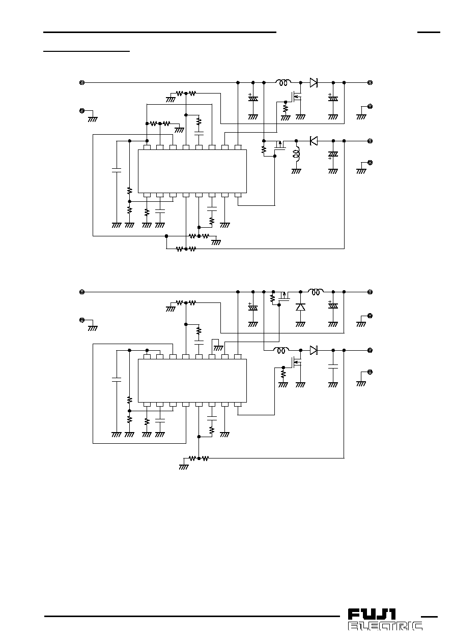
10.Application circuit
FA7703
16
15
14
13
12
11
10
9
1
2
3
4
5
6
7
8
RT
CS
DT 2
IN2+
IN2-
FB2
G ND
O UT 2
REG
DT 1
REF
IN1-
FB1
SEL1
O UT 1
VCC
Vin
2.5 to 8.0V
10V/100mA
-7.5V/100mA
9k
1k
1k
11k
10k
2200pF
0.1
µ
F
11k
10k
10k
1
µ
F
1k
16k
10k
10k
22k
4700pF
Vin
8 to 18V
5V/500mA
30V/20mA
FA7704
16
15
14
13
12
11
10
9
1
2
3
4
5
6
7
8
RT
CS
DT 2
IN2+
IN2-
FB2
G ND
O UT 2
REG
DT 1
REF
IN1-
FB1
SEL1
O UT 1
VCC
4k
1k
10k
4700pF
0.1
µ
F
10k
11k
10k
1.5k
0.1
µ
F
43k
10k
4700pF