DS04-27241-1E
FUJITSU SEMICONDUCTOR
DATA SHEET
ASSP for Power Supply Applications (Secondary battery)
DC/DC Converter IC for Charging
Li-ion Battery
MB39A114
s
s
s
s
DESCRIPTION
The MB39A114 is a DC/DC converter IC of pulse width modulation (PWM) type for charging, capable of inde-
pendently controlling the output voltage and output current. It is suitable for down conversion.
MB39A114 can dynamically control the secondary battery's charge current by detecting a voltage drop in an AC
adapter to keep its power constant (dynamically-controlled charging) .
This IC can easily set the charge current value, making it ideal for use as a built-in charging device in products
such as notebook PC.
s
s
s
s
FEATURES
∑ Built-in constant current control circuit in 2-system.
∑ Analog control of charge current value is possible. (
+
INE1 terminal and
+
INE2 terminal)
∑ Built-in AC adapter detection function (When V
CC
is lower than the battery voltage
+
0.2 V, output is fixed in the off.)
∑ Constant voltage control state detection function (CVM terminal) enables prevention of mis-detection for full
charge.
∑ Built-in overvoltage detection function (OVP terminal) of charge voltage
(Continued)
s
s
s
s
PACKAGE
24-pin plastic SSOP
(FPT-24P-M03)

MB39A114
2
(Continued)
∑ Wide range of operating power-supply voltage range : 8 V to 25 V
∑ Built-in output setting resistor
∑ Built-in switching function (SEL terminal) of output setting voltage 16.8 V or 12.6 V
∑ Output voltage setting accuracy
:
±
0.74
%
(Ta
=
-
10
∞
C to
+
85
∞
C)
∑ Built-in high accuracy current detection amplifier :
±
5
%
(At the input voltage difference of 100 mV) ,
±
15% (At the input voltage difference of 20 mV)
∑ Output voltage setting resistor is open to enable prevention of invalidity current at IC standby (I
CC
=
0
µ
A Typ).
∑ Oscillation frequency range
: 100 kHz to 500 kHz
∑ Built-in current detection Amp with wide in-phase input voltage range : 0 V to V
CC
∑ Built-in soft-start function independent of loads
∑ Built-in standby current function
: 0
µ
A (Typ)
∑ Built-in totem-pole type output stage supporting Pch MOS FET devices.

MB39A114
4
s
s
s
s
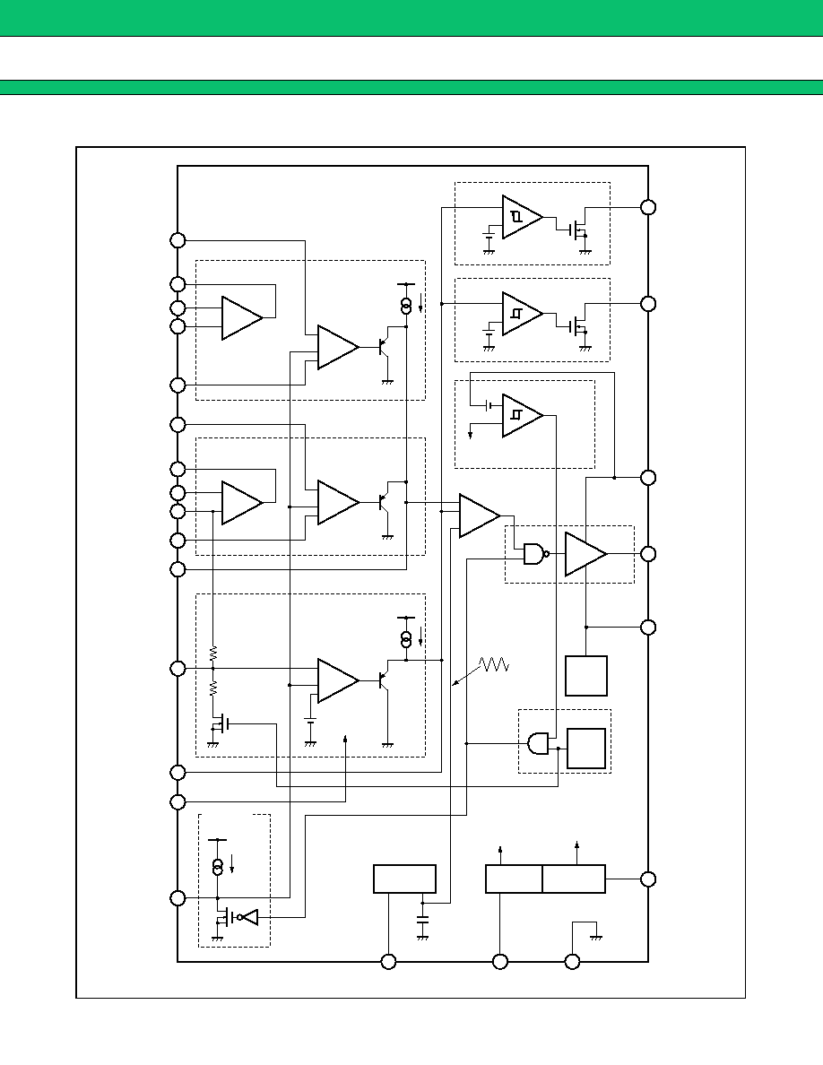
PIN DESCRIPTION
Pin No.
Symbol
I/O
Description
1
-
INC2
I
Current detection amplifier (Current Amp2) inverted input terminal
2
OUTC2
O
Current detection amplifier (Current Amp2) output terminal
3
+
INE2
I
Error amplifier (Error Amp2) non-inverted input terminal
4
-
INE2
I
Error amplifier (Error Amp2) inverted input terminal
5
CVM
O
Open drain type output terminal of constant voltage control state detec-
tion comparator (CV Comp.)
6
VREF
O
Reference voltage output terminal
7
FB12
O
Error amplifier (Error Amp1, Error Amp2) output terminal
8
-
INE1
I
Error amplifier (Error Amp1) inverted input terminal
9
+
INE1
I
Error amplifier (Error Amp1) non-inverted input terminal
10
OUTC1
O
Current detection amplifier (Current Amp1) output terminal
11
SEL
O
Charge voltage setting switch terminal (3 cell or 4 cell)
"H" level in SEL terminal : charge voltage setting 16.8 V (4 Cell)
"L" level in SEL terminal : charge voltage setting 12.6 V (3 Cell)
12
-
INC1
I
Current detection amplifier (Current Amp1) inverted input terminal
13
+
INC1
I
Current detection amplifier (Current Amp1) non-inverted input terminal
14
CTL
I
Power-supply control terminal
Setting the CTL terminal at "L" level places the IC in the standby mode.
15
FB3
O
Error amplifier (Error Amp3) output terminal
16
-
INE3
I
Error amplifier (Error Amp3) inverted input terminal
17
RT
Triangular wave oscillation frequency setting resistor connection
terminal
18
OVP
O
Open drain type output terminal overvoltage detection comparator (OV
Comp.)
19
VH
O
Power supply terminal for FET drive circuit (VH
=
V
CC
-
6 V)
20
OUT
O
External FET gate drive terminal
21
VCC
Power supply terminal for reference power supply, control circuit and
output circuit
22
CS
Soft-start capacitor connection terminal
23
GND
Ground terminal
24
+
INC2
I
Current detection amplifier (Current Amp2) non-inverted input terminal