DS07-16502-3E
FUJITSU SEMICONDUCTOR
DATA SHEET
32-Bit Proprietary Microcontroller
CMOS
FR60 MB91301 Series
MB91302A/V301A
DESCRIPTION
The MB91301 series are a line of microcontrollers based on a 32-bit RISC CPU core (FR family) , incorporating
a variety of I/O resources and a bus control mechanism for embedded control that requires the processing of a
high-performance, fast CPU as well as an SDRAM interface that can connect SDRAM directly to the chip.
The large address space supported by the 32-bit CPU addressing means that operation is primarily based on
external bus access although instruction cache memory of 4 Kbytes and RAM of 4 Kbytes( for data) are included
for high-speed execution of CPU instructions.
The MB91302A and MB91V301A are FR60 products based on the FR30/40 CPU with enhanced bus access for
higher speed operation. The device specifications include a D/A converter to facilitate motor control and are ideal
for use in DVD players that support fly-by transfer.
FEATURES
The MB91301 series is a line of ICs with various programs embedded in internal ROM.
(Continued)
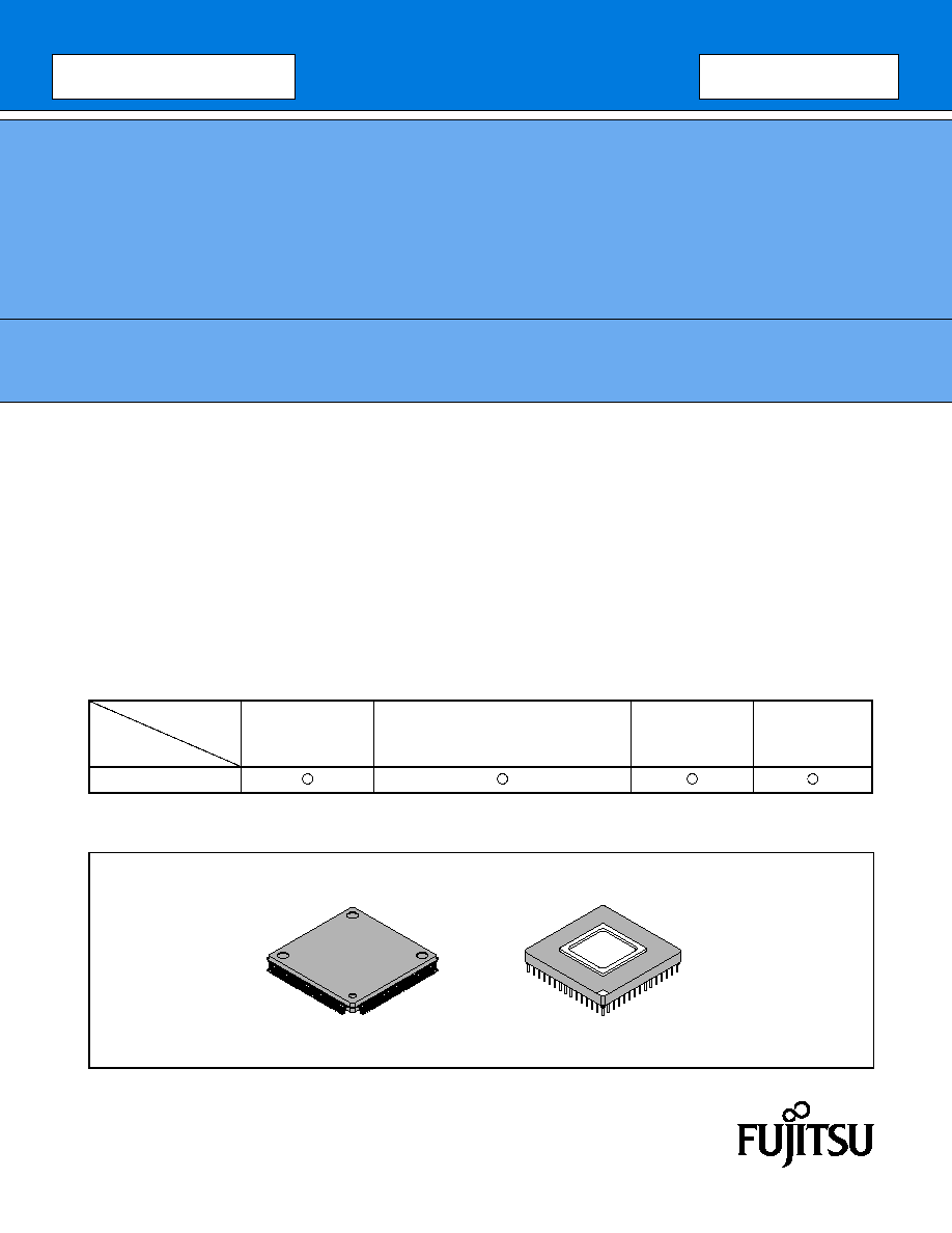
PACKAGES
Built-in the real
time OS version
Built-in IPL
(Internal Program Loader) version
User ROM
version
Without ROM
version
MB91302A
ROM variation
Product name
144-pin, Plastic LQFP
179-pin, Ceramic PGA
(FPT-144P-M12)
(PGA-179C-A03)

MB91301 Series
2
1.
FR CPU
� 32-bit RISC, load/store architecture, 5-stage pipeline
� 68 MHz internal operating frequency (Max) [external (Max) 68 MHz] (when using PLL with base frequency
(Max)
=
17 MHz)
� General purpose registers : 32 bits
�
16
� 16-bit fixed length instructions (basic instructions) , 1 instruction per cycle
� Instruction set optimized for embedded applications: Memory-to-memory transfer, bit manipulation, barrel shift
etc.
� Instructions adapted for high-level languages : Function entry/exit instructions, multiple-register load/store
instructions
� Easier assembler coding : Register interlock function
� Branch instructions with delay slots : Reduced overhead time in branch executions
� Built-in multiplier with instruction-level support
Signed 32-bit multiplication : 5 cycles
Signed 16-bit multiplication : 3 cycles
� Interrupt (PC, PS save) : 6 cycles, 16 priority levels
2.
Bus interface
� Operating frequency : Max 68 MHz (when using SDRAM)
� Full 24-bit address output (16 Mbytes memory space)
� 8-bit, 16-bit or 32-bit data input/output
� Built-in pre-fetch buffer
� Unused data and address pins can be used as general-purpose input/output ports.
� Eight fully independent chip select outputs, can be set in minimum 64 Kbytes units.
� Supports the following memory interfaces
Asynchronous SRAM, asynchronous ROM/Flash
Page mode ROM/Flash ROM (selectable page size
=
1, 2, 4, or 8)
Burst mode ROM/Flash ROM (MBM29BL160D/161D/162D)
� SDRAM (FCRAM Type, CAS Latency 1 to 8, 2/4 bank products.)
� Address/Data multiplex bus (only 8/16-bit width)
� Basic bus cycle : 2 cycles
� Automatic wait cycle generation function can insert wait cycles, independently programmable for each memory
area.
� RDY input for external wait cycles
� Endian setting of byte ordering (Big/Little)
CS0 area only for big endian
� Prohibition setting of write (only for Read)
� Permission/prohibition setting of fetch into built-in cache
� Permission/prohibition setting of prefetch function
� DMA supports fly-by transfer with independent I/O wait control
� External bus arbitration can be used using BRQ and BGRNT.
3.
Built-in memory
� 4 Kbytes DATA RAM
� 4 Kbytes RAM (MB91302A)
(Continued)

MB91301 Series
3
4.
Instruction cache
� Size : 4 Kbytes
� 2-way set associative
� 128 blocks/way, 4 entries/block
� Lock function enables program code to be made cache-resident
� Areas not used for instruction cache can be used as instruction RAM
5.
DMAC (DMA Controller)
� 5-channel (2-channel external-to-external)
� 3 transfer triggers : External pin, internal peripheral, software
� Capable of selecting an internal peripheral as a transfer source freely for each channel
� Addressing using 32-bit full addressing mode (increment, decrement, fixed)
� Transfer modes : Demand transfer, burst transfer, step transfer, or block transfer
� Supports fly-by transfer (between external I/O and memory)
� Selectable transfer data size : 8, 16, or 32-bit
6.
Bit search module
� Searches words from MSB for position of first 1/0 bit value change
7.
Reload Timers
� 16-bit timer : 3 channels
� Internal clock : 2 clock cycle resolution, divide by 2/8/32 selective
8.
UART
� Full duplex, double buffer UART
� Independent 3 channels
� Data length : 7 bits to 9 bits (without parity) , 6 bits to 8 bits (with parity)
� Asynchronous (start-stop synchronized) or CLK-synchronous communications selectable
Multi-processor mode
� Built-in 16-bit timer (U-TIMER) as a baud rate generator to generate arbitrary baud rates
� External clock can be used as transfer clock
� Variety of error detection functions (parity, frame, overrun)
9.
Interrupt controller
� External interrupt input : 1 non-maskable interrupt pin and 8 normal interrupt pins (INT0 to INT7)
� Internal internal resources : UART, DMAC, A/D, U-TIMER, Delay interrupt, I
2
C, Free-run timer, Input capture
� Programmable priorities (16 levels) for all interrupts except the non-maskable interrupt
10. A/D converter
� 10-bit resolution, 4 channels
� Successive approximation type, conversion time : 4.1
�
s at 34 MHz
� Built-in sample and hold circuit
� Conversion modes : Single conversion mode, scan conversion mode and repeat conversion mode selectable
� Conversion triggers : Software, external trigger and built-in timer selectable
11. I
2
C* interface
� Internal 2-channels master/slave transmit/receive
� Internal arbitration function, clock synch function
12. Free-run timer
� 16 bit : 1channel
(Continued)

MB91301 Series
4
(Continued)
13. Input capture
� 4 channels
14. Other interval timers
� 16-bit timer : 3 channels (U-TIMER)
� PPG timer : 4 channels
� Watchdog timer : 1 channel
15. Other features
� Reset resources : watchdog timer/software reset/external reset (INIT pin)
� Power-saving modes : Stop mode, sleep mode
� Clock control
Gear function : Allows arbitrary different operating clock frequencies to be set for the CPU and peripherals.
You can select one of the 16 gear clock factors of 1/1 to 1/16. PLL multiplication can also be selected. Note,
however, that peripherals operate at a maximum of 34 MHz.
� CMOS technology : 0.25
�
m
� Power supply (analog power supply): 3.3 V
�
0.3 V (internal regulator used)
* : Purchase of Fujitsu I
2
C components conveys a license under the Philips I
2
C Patent Rights to use, these
components in an I
2
C system provided that the system conforms to the I
2
C Standard Specification as defined
by Philips.
PRODUCT LINEUP
*1 : The Fujitsu product of real time OS REALOS/FR by conforming to the
�
ITRON 3.0 is stored and optimized
with the MB91302A.
*2 : The ROM stores the IPL (Internal Program Loader) . Loading various programs can be executed from the
external system by the internal UART/SIO. Using this function, for example, writing on board to the Flash
memory connected to the external can be executed.
MB91302A
MB91V301A
Type
Mask ROM product
(for volume production)
Evaluation version
(For evaluation and develop-
ment)
RAM
4 Kbytes
(only for data)
16 Kbytes
(data 8 KB
+
8 KB)
ROM
4 Kbytes
ROM has non-ROM model, the optimal real time
OS internal model*
1
, and the IPL (Internal Program
Loader) internal model*
2
by adding the user ROM
model.
8 Kbytes (RAM)
DSU
DSU4
Package
LQFP-144
(0.4 mm pitch)
PGA-179

MB91301 Series
5
PIN ASSIGNMENTS
� MB91302A
(TOP VIEW)
(FPT-144P-M12)
1
2
3
4
5
6
7
8
9
10
11
12
13
14
15
16
17
18
19
20
21
22
23
24
25
26
27
28
29
30
31
32
33
34
35
36
37
38
39
40
41
42
43
44
45
46
47
48
49
50
51
52
53
54
55
56
57
58
59
60
61
62
63
64
65
66
67
68
69
70
71
72
108
107
106
105
104
103
102
101
100
99
98
97
96
95
94
93
92
91
90
89
88
87
86
85
84
83
82
81
80
79
78
77
76
75
74
73
144
143
142
141
140
139
138
137
136
135
134
133
132
131
130
129
128
127
126
125
124
123
122
121
120
119
118
117
116
115
114
113
112
111
110
109
P13/D11
P14/D12
P15/D13
P16/D14
P17/D15
V
SS
V
CC
P20/D16
P21/D17
P22/D18
P23/D19
P24/D20
P25/D21
P26/D22
P27/D23
V
SS
V
CC
D24
D25
D26
D27
D28
D29
D30
D31
V
SS
V
CC
P80/RDY
P81/BGRNT
P82/BRQ
RD
DQMUU/WR0(UUB)
P85/DQMUL/WR1(ULB)
P86/DQMLU/WR2(LUB)
P87/DQMLL/WR3(LLB)
P90/SYSCLK
D10/P12
D09/P11
D08/P10
V
CC
V
SS
D07/P07
D06/P06
D05/P05
D04/P04
D03/P03
D02/P02
D01/P01
D00/P00
V
CC
V
SS
CS7/PA7
CS6/PA6
CS5/PPG2/PA
5
CS4/TRG2/PA
4
CS3/PA3
CS2/PA2
CS1/PA1
CS0/PA0
V
CC
NMI
INIT
MD2
MD1
MD0
V
CC
V
SS
X1
X0
V
CC
IORD/PB7
IOWR/PB6
DEOP1/PPG1/PB5
DACK1/TRG1/PB4
DREQ1/PB3
DEOP0/PB2
DACK0/PB1
DREQ0/PB0
C
V
SS
TIN2/TRG3/PH2
TIN1/PPG3/PH1
TIN0/PH0
TRG0/PJ7
PPG0/PJ6
SCK1/PJ5
SOT1/PJ4
SIN1/PJ3
SCK0/PJ2
SOT0/PJ1
SIN0/PJ0
V
CC
INT7/SCK2/PG7
INT6/SOT2/PG6
INT5/SIN2/PG5
INT4/ATG/PG4/FRCK
INT3/PG3/ICU3
INT2/PG2/ICU2
INT1/PG1/ICU1
INT0/PG0/ICU0
AV
SS
/AVRL
AN0
AN1
AN2
AN3
AVR
AVRH
AV
CC
P91/MCLKE
P92/MCLK
P93
P
94/SRAS/LBA/AS
P95/SCAS/BAA
P96/SWE/WR
V
SS
V
CC
A00
A01
A02
A03
A04
A05
A06
A07
V
SS
V
CC
A08
A09
A10
A11
A12
A13
A14
A15
V
SS
P60/A16
P61/A17
P62/A18
P63/A19
P64/A20/SDA0
P65/A21/SCL0
P66/A22/SDA1
P67/A23/SCL1
V
CC