SD833-06
(3A)
(60V / 3A )
Features
Low V
F
High voltage 60V
Low height : 1.2mm max.
Small mounting area
Good heat radiation
characteristic
Applications
High frequency operation
DC-DC converters
AC adapter
Reverse battery protection
Oring diode for redundant
power system
Maximum ratings and characteristics
Absolute maximum ratings
Item
Repetitive peak surge reverse voltage
Repetitive peak reverse voltage
Average output current
Non-repetitive surge current
Operating junction temperature
Storage temperature
Symbol
V
RSM
V
RRM
I
o
I
FSM
T
j
T
stg
Conditions
Sine wave
10ms, 1shot
-40 to +150
Unit
V
V
A
A
∞C
∞C
Electrical characteristics (Tc=25∞C Unless otherwise specified )
Item
Forward voltage drop
Reverse current
Symbol
V
F
I
R
Conditions
I
FM
=2.5A
V
R
=V
RRM
Max.
0.58
1.0
Unit
V
mA
Square wave, duty=
1/2
Tl=121∞C
Rating
60
60
3
60
+150
Schottky barrier diode
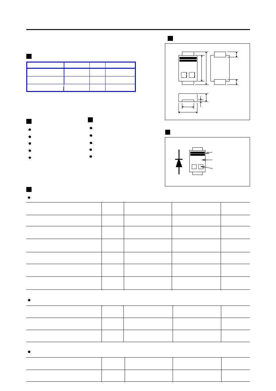
Outline drawings, mm
Electrical characteristics (Tc=25∞C Unless otherwise specified )
Major characteristics
Item
Thermal resistance
Symbol
Rth(j-c)
Condition
Junction to case
Max.
12.0
Unit
∞C/W
Characteristics
SD833-06
Units Condition
V
RRM
60
V
V
F
0.5
V
Tj=125∞C, typ
I
O
3
A
tw=500ns, duty=1/40
Marking
1.5
2.5
1.2
max.
0.2
4.0
5.0
0.8
0.8
B C
Type No
Cathode mark
Lot. No
B C

SD833-06 (3A)
Characteristics
(60V / 3A )
0.01
0.1
1
10
0.0
0.1
0.2
0.3
0.4
0.5
0.6
0.7
0.8
0.9
1.0
Tj=100∞C
Tj=25∞C
Tj=125∞C
Tj=150∞C
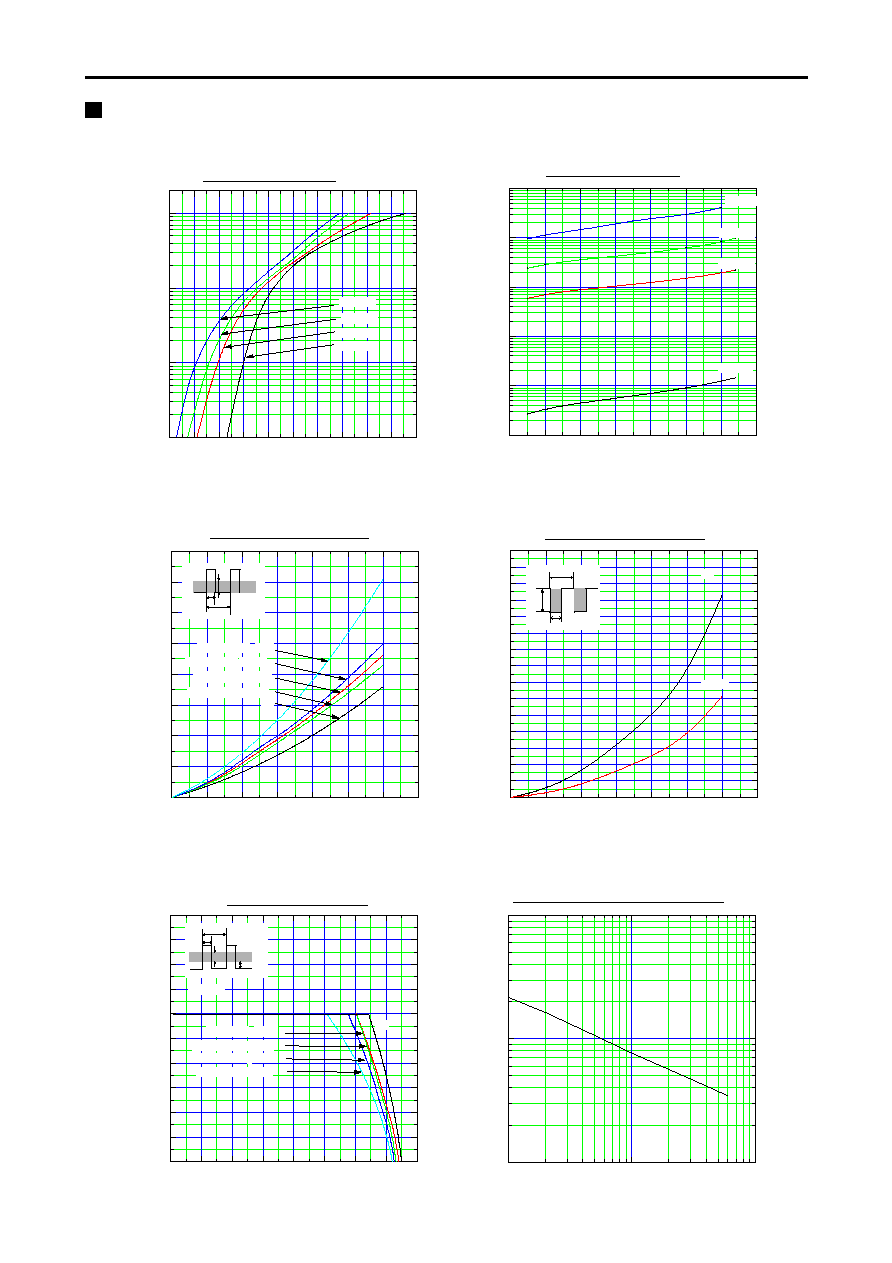
Forward Characteristic (typ.)
IF Forward Current (A)
VF Forward Voltage (V)
0
10
20
30
40
50
60
70
10
-3
10
-2
10
-1
10
0
10
1
10
2
Reverse Characteristic (typ.)
Tj= 25∞C
Tj=100∞C
Tj=125∞C
Tj=150∞C
IR Reverse Current (mA)
VR Reverse Voltage (V)
0.0
0.5
1.0
1.5
2.0
2.5
3.0
3.5
0.0
0.5
1.0
1.5
2.0
2.5
3.0
3.5
4.0
Square wave
=180∞
Sine wave
=180∞
Square wave
=120∞
DC
Square wave
=60∞
Forward Power Dissipation
WF Forward Power Dissipation (W)
Io Average Forward Current (A)
0
10
20
30
40
50
60
70
0.0
0.2
0.4
0.6
0.8
1.0
1.2
1.4
1.6
1.8
2.0
2.2
2.4
2.6
2.8
3.0
Reverse Power Dissipation
=180∞
DC
PR Reverse Power Dissipation (W)
VR Reverse Voltage (V)
0.0
0.5
1.0
1.5
2.0
2.5
3.0
3.5
4.0
4.5
5.0
0
20
40
60
80
100
120
140
160
VR=30V
Square wave
=60∞
Square wave
=120∞
Square wave
=180∞
Sine wave
=180∞
DC
Current Derating (Io-Tl)
Tl Lead Temperature (∞C)
Io Average Output Current (A)
1
10
100
10
100
1000
Junction Capacitance Characteristic(typ.)
Cj Junction Capacitance (pF)
VR Reverse Voltage (V)
360∞
Io
360∞
V
R
VR=30V
360∞
Io

SD833-06 (3A)
(60V / 3A )
1
10
1
10
100
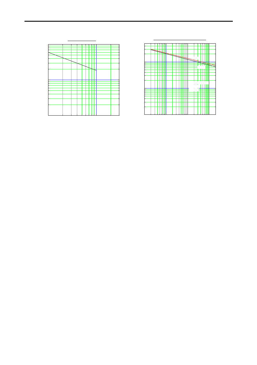
Surge Capability
I FSM Peak Half - Wave Current (A)
Number of Cycles at 50Hz
1
10
100
1000
1
10
100
With Glass Epoxy
P.C Board
t=0.8mm
Rth(l-a)
Rth(j-a)
Thermal Resistance Print Land
Thermal Resistance (∞C/W)
Print Land Area (mm≤)
