±
0.5
±
0.3
±
0.3
±
0.2
±
0.2
+0.2
--0.1
4.5
1.32
2.7
5.08
1.2
10
0.4
0.8
0.9
9.3
1.5
3.0
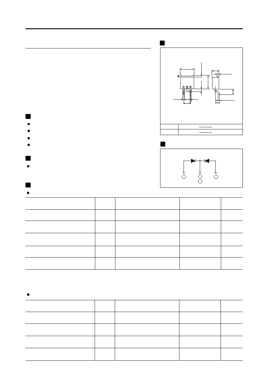
1. Gate
2, 4. Drain
3. Source
+0.5
+0.2
Max
TS902C3
(10A)
( 300V / 10A )
LOW LOSS SUPER HIGH SPEED RECTIFIER
Outline drawings, mm
Features
Surface-mount device
Low V
F
Super high speed switching
High reliability by planer design
Applications
High speed power switching
Maximum ratings and characteristics
Absolute maximum ratings
Item
Repetitive peak reverse voltage
Average output current
Surge current
Operating junction temperature
Storage temperature
Symbol
V
RRM
I
O
I
FSM
T
j
T
stg
Conditions
40
-40 to +150
-40 to +150
Unit
V
A
A
∞C
∞C
Electrical characteristics (Ta=25∞C Unless otherwise specified )
Item
Forward voltage drop
Reverse current
Reverse recovery time
Thermal resistance
Symbol
V
FM
I
RRM
t
rr
R
th(j-c)
Conditions
I
FM
=5.0A
V
R
=V
RRM
I
F
=0.1A, I
R
=0.2A, I
rec
=0.05A
Junction to case
Max.
1.2
100
35
2.5*
Unit
V
µA
ns
∞C/W
Square wave, duty=1/2, Tc=125∞C
Sine wave 10ms
Rating
300
10*
Connection diagram
*
Average forward current of centertap full wave connection
1
3
JEDEC
EIAJ
2
4

TS902C3 (10A)
(300V / 10A )
Characteristics
Forward characteristics
V
F
[V]
Reverse characteristics
V
R
[V]
I
F
[A]
I
R
[
µ
A]
Forward power dissipation
I
o
[A]
W
F
[W]
0 2 4 6
Junction capacitance characteristics
C
j
[pF]
V
R
[V]
Output current-case temperature
T
c
[∞C]
I
o
[A]
0 0.5 1.0 1.5
10
5
3
1
0.5
0.3
0.1
1000
300
100
30
10
3
1
6
4
2
0
30
10
5
3
1
0 100 200 300
Reverse power dissipation
V
R
[V]
W
R
[W]
0 100 200 300
1.0
0.5
0
150
100
50
0
0 2 4 6 8 10 12 14
5 10 30 50 100


