
YG233C2,N2,D2
(8A)
(200V / 8A)
FAST RECOVERY DIODE
Outline drawings, mm
Item
Repetitive peak reverse voltage
Non-repetitive peak reverse voltage
Isolating voltage
Average output current
Surge current
Operating junction temperature
Storage temperature
Symbol
V
RRM
V
RSM
V
iso
I
O
I
FSM
T
j
T
stg
Conditions
30
+150
-40 to +150
Unit
V
V
V
A
A
∞C
∞C
Electrical characteristics (Ta=25∞C Unless otherwise specified )
Item
Forward voltage drop **
Reverse current **
Reverse recovery time
Thermal resistance
Symbol
V
FM
I
RRM
t
rr
R
th(j-c)
Conditions
I
FM
=2.0A
V
R
=V
RRM
I
F
=0.1A, I
R
=0.1A
Junction to case
Max.
1.4
500
0.1
3.5
Unit
V
µA
µs
∞C/W
Square wave, duty=1/2, Tc=95∞C
Sine wave 10ms
Rating
200
200
1500
8*
Connection diagram
*
Average forward current of centertap full wave connection
JEDEC
EIAJ
SC-67
10
±0.5
2.54
±0.2
0.7
±0.2
1.2
±0.2
2.7
±0.2
0.6
2.7
±0.2
4.5
±0.2
3.7
±0.2
15
±0.3
2.7
±0.2
13
Min
6.3
¯3.2
+0.2
-0.1
+0.2
-0
Applications
High speed switching
Maximum ratings and characteristics
Absolute maximum ratings
Features
Insulated package by fully molding
High voltage by mesa design
High reliability
Mechanical characteristics
Mounting torque
Approximate weight
N∑m
g
0.3 to 0.5
2.3
Recommended torque
**
Rating per element
Terminals-to-Case, AC.1min
YG233C2
YG233N2
YG233D2
1
1
1
2
2
2
3
3
3
1
2
3
YG233C2,N2,D2 (8A)
(200V / 8A )
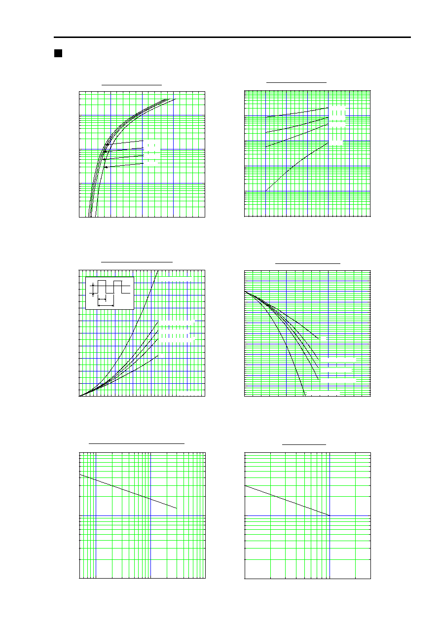
Characteristics
0.01
0.1
1
10
0
1
2
3
4
Tj=100∞C
Tj=25∞C
Tj=125∞C
Tj=150∞C
Forward Characteristic (typ.)
IF Forward Current (A)
VF Forward Voltage (V)
0
50
100
150
200
250
300
10
-3
10
-2
10
-1
10
0
10
1
10
2
Tj=25∞C
Tj=100∞C
Tj=125∞C
Tj=150∞C
Reverse Characteristic (typ.)
IR Reverse Current (
µ
A)
VR Reverse Voltage (V)
0
1
2
3
4
5
6
7
0
2
4
6
8
10
12
14
16
18
20
Per 1element
DC
Square wave
=180
o
Sine wave
=180
o
Square wave
=120
o
Square wave
=60
o
Forward Power Dissipation
WF Forward Power Dissipation (W)
Io Average Forward Current (A)
12345678901234567
12345678901234567
12345678901234567
12345678901234567
360
o
Io
0
5
10
15
50
60
70
80
90
100
110
120
130
140
150
160
170
Square wave
=60∞
Square wave
=120∞
Square wave
=180∞
Sine wave
=180∞
:Conduction angle of forward current for each rectifier element
Io:Output current of center-tap full wave connection
DC
Current Derating (Io-Tc)
Tc Case Temperature (∞C)
Io Average Output Current (A)
10
100
1000
1
10
100
Junction Capacitance Characteristic (typ.)
Cj Junction Capacitance (pF)
VR Reverse Voltage (V)
1
10
1
10
100
Surge Capability
I FSM Peak Half - Wave Current (A)
Number of Cycles at 50Hz
