YG901C3R
LLD
(300V / 5A TO-22OF15)
LOW LOSS SUPER HIGH SPEED DIODE
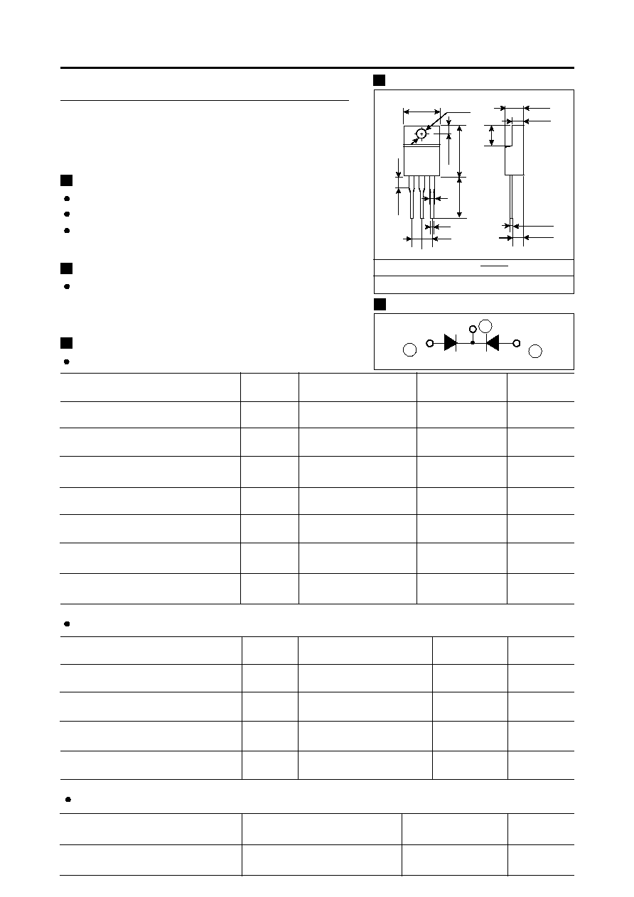
Outline Drawings
JEDEC
EIAJ
SC-67
Features
Low V
F
Super high speed switching.
High reaibility by planer design.
Applications
High speed power switching
Connection Diagram
Maximum Ratings and Characteristics
Absolute Maximum Ratings
Item
Repetitive Peak
Reverse Voltage
Repetitive Peak Surge Reverse Voltage
Isolation Voltage
Average Output Current
S
urge Current
Operating Junction Temperature
Storage Temperature
Symbol
V
RRM
V
RSM
V
iso
I
O
I
FSM
T
j
T
stg
Conditions
duty=1/2, Tc=105∞C
Square wave
Sine wave 10ms
Rating
300
300
1500
5*
25
-40 to +150
-40 to +150
Unit
V
V
V
A
A
∞C
∞C
Electrical Characteristics (Ta=25∞C Unless otherwise specified )
Item
Forward Voltage Drop **
Reverse Current **
Reverse recovery time
Thermal Resistance
Symbol
V
F
I
R
trr
R
th(j-c)
Conditions
I
F
=2.5A
V
R
=V
RRM
I
F
=0.1A,I
R
=0.2A,Irec=0.05A
Junction to case
Max.
1.2
100
35
5.0
Unit
V
µA
ns
∞C/W
Terminals to Case,
AC. 1min.
Mechanical Characteristics
Mounting torque
Weight
Recommended torque
0.3 to 0.5
2.3
N ∑ m
g
*
Out put current of centertap full wave connection.
1
2
3
**
Rating per element
10
±0.5
2.54
±0.2
0.7
±0.2
1.2
±0.2
2.7
±0.2
0.6
2.7
±0.2
4.5
±0.2
3.7
±0.2
15
±0.3
2.7
±0.2
13
Min
6.3
¯3.2
+0.2
-0.1
+0.2
-0

Characteristics
LLD ( 300V / 5A TO-220F15)
YG901C3R (5A)
0.1
1
10
100
0.4
0.6
0.8
1.0
1.2
1.4
1.6
1.8
2.0
o
C
o
C
o
C
o
C
Tj=150
Tj=125
Tj=100
Tj=25
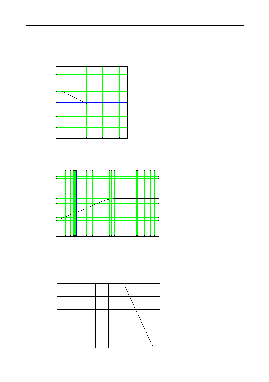
Forward Characteristic
(typ.)
I F Forward Current (A)
V F Forward Voltage (V)
50
100
150
200
250
300
10
-1
10
0
10
1
10
2
10
3
10
4
Tj=150
o
C
Tj=125
o
C
Reverse Characteristic (typ.)
Tj= 25
o
C
Tj=100
o
C
I R Reverse Current (
µ
A)
V R Reverse Voltage (V)
0.0
0.5
1.0
1.5
2.0
2.5
0.0
0.5
1.0
1.5
2.0
2.5
3.0
3.5
4.0
4.5
Per 1element
DC
Square wave
=180
o
Sine wave
=180
o
Square wave
=120
o
Square wave
=60
o
Forward Power Dissipation
W F Forward Power Dissipation (W)
I o Average Forward Current (A)
0
50
100
150
200
250
300
0.0
0.1
0.2
0.3
0.4
0.5
0.6
0.7
Reverse Power Dissipation
=180
o
DC
P R Reverse Power Dissipation (W)
V R Reverse Voltage (V)
0
1
2
3
4
5
6
7
8
50
60
70
80
90
100
110
120
130
140
150
160
:Conduction angle of forward current for each rectifier element
Io:Output current of center-tap full wave connection
Square wave
=120
o
Square wave
=60
o
Square wave
=180
o
Sine wave
=180
o
DC
Current Derating (Io-Tc)
T c Case Temperature (
o
C)
I o Average Output Current (A)
1
10
100
0.1
1
10
100
Junction Capacitance Characteristic
(typ.)
C j Junction Capacitance (pF)
V R Reverse Voltage (V)
360∞
Io
360∞
V R
360∞
Io
VR=300V
YG901C3R (5A)
LLD ( 300V / 5A TO-220F15)
DERATING
ratio to rated current (%)
Case temperature (∞C)
0 20 40 60 80 100 120 140 160
20
40
0
60
80
100
1
10
100
1
10
100
Surge Capability
I FSM Peak Half - Wave Current (A)
Number of Cycles at 50Hz
10
-3
10
-2
10
-1
10
0
10
1
10
2
10
-1
10
0
10
1
10
2
Transient Thermal Impedance
Transient Thermal Impedance (
o
C/ W)
t Time (sec)