 | –≠–ª–µ–∫—Ç—Ä–æ–Ω–Ω—ã–π –∫–æ–º–ø–æ–Ω–µ–Ω—Ç: 29LV650 | –°–∫–∞—á–∞—Ç—å:  PDF PDF  ZIP ZIP |

DS05-20882-2E
FUJITSU SEMICONDUCTOR
DATA SHEET
FLASH MEMORY
CMOS
64M (4M
◊
16) BIT
MBM29LV650UE/651UE
-90/12
s
s
s
s
DESCRIPTION
The MBM29LV650UE/651UE is a 64M-bit, 3.0 V-only Flash memory organized as 4M words of 16 bits each. The
device is designed to be programmed in system with the standard system 3.0 V V
CC
supply. 12.0 V V
PP
and
5.0 V V
CC
are not required for write or erase operations. The devices can also be reprogrammed in standard
EPROM programmers.
To eliminate bus contention the devices have separate chip enable (CE), write enable (WE), and output enable
(OE) controls.
The MBM29LV650UE/651UE is entirely command set compatible with JEDEC single-power-supply Flash stan-
dard. Commands are written to the command register using standard microprocessor write timings. Register
contents serve as input to an internal state-machine which controls the erase and programming circuitry. Write
cycles also internally latch addresses and data needed for the programming and erase operations.
Typically, each sector can be programmed and verified in about 0.5 seconds.
(Continued)
s
s
s
s
PRODUCT LINEUP
s
s
s
s
PACKAGES
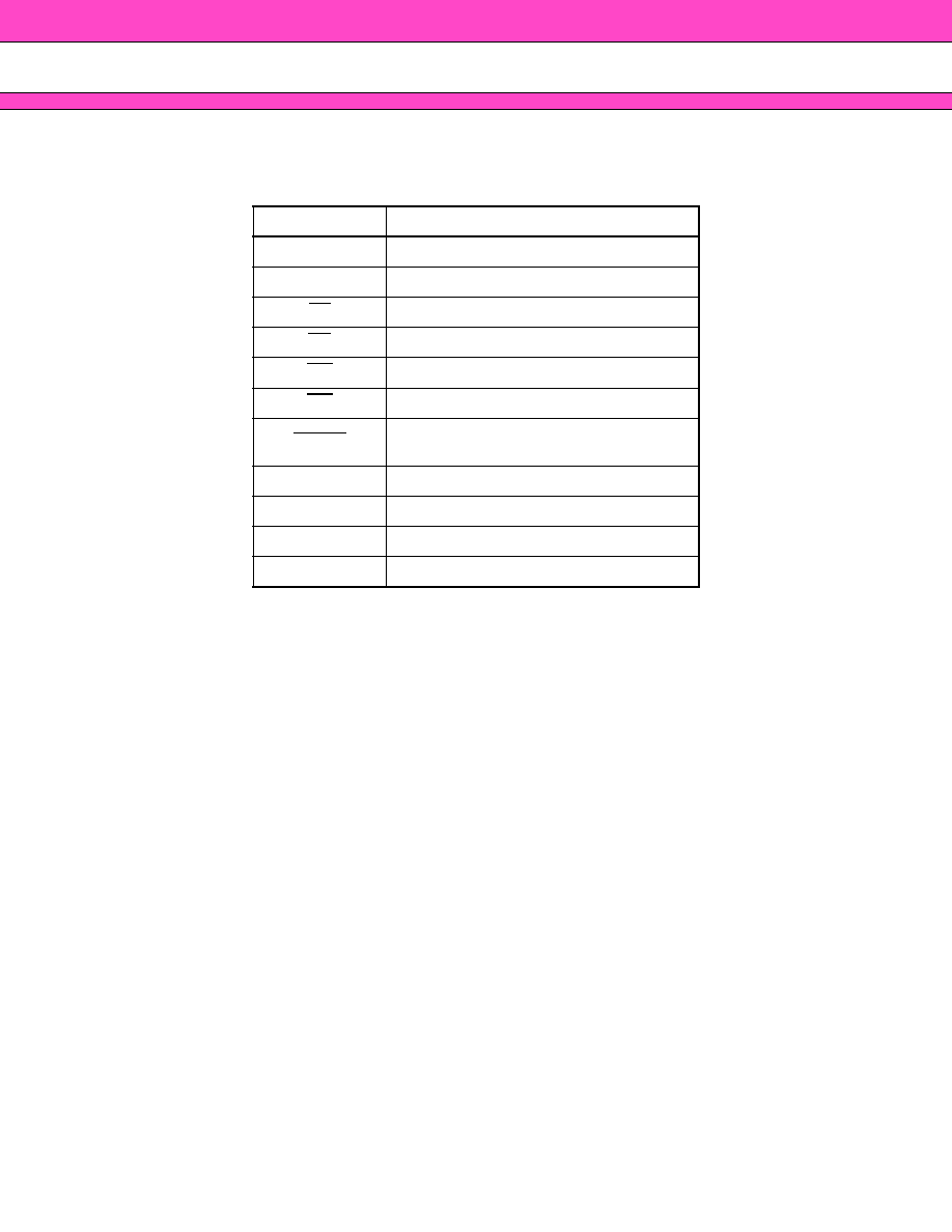
Part No.
MBM29LV650UE/651UE
Ordering Part No.
V
CC
= 3.3 V
90
--
V
CC
= 3.0 V
--
12
Max. Address Access Time (ns)
90
120
Max. CE Access Time (ns)
90
120
Max. OE Access Time (ns)
35
50
+0.3 V
≠0.3 V
+0.6 V
≠0.3 V
(FPT-48P-M20)
(FPT-48P-M19)
Marking Side
Marking Side
48-pin plastic TSOP (I)

MBM29LV650UE/651UE-
90/12
2
(Continued)
A sector is typically erased and verified in 1.0 second. (If already completely preprogrammed.)
The device also features a sector erase architecture. The sector mode allows each sector to be erased and
reprogrammed without affecting other sectors. The MBM29LV650UE/651UE is erased when shipped from the
factory.
Internally generated and regulated voltages are provided for the program and erase operations. A low V
CC
detector automatically inhibits write operations on the loss of power. The end of program or erase is detected
by Data Polling of DQ
7
, by the Toggle Bit feature on DQ
6
. Once the end of a program or erase cycle has been
completed, the devices internally reset to the read mode.
The devices electrically erase all bits within a sector simultaneously via Fowler-Nordhiem tunneling. The words
are programmed one word at a time using the EPROM programming mechanism of hot electron injection.
s
s
s
s
FEATURES
∑ 0.23
µ
m Process Technology
∑ Single 3.0 V read, program and erase
Minimizes system level power requirements
∑ Compatible with JEDEC-standards
Uses same software commands with single-power supply Flash
∑ Address don't care during the command sequence
∑ Industry-standard pinouts
48-pin TSOP (I) (Package suffix: TN - Normal Bend Type, TR - Reversed Bend Type)
∑ Minimum 100,000 program/erase cycles
∑ High performance
90 ns maximum access time
∑ Flexible sector architecture
One hundred twenty-eight 32K word sectors
Any combination of sectors can be concurrently erased. Also supports full chip erase
∑ Hidden ROM (Hi-ROM) region
128 word of Hi-ROM, accessible through a new "Hi-ROM Enable" command sequence
Factory serialized and protected to provide a secure electronic serial number (ESN)
∑ WP input pin
At V
IL
, allows protection of first or last 32K word sector, regardless of sector protection/unprotection status
At V
IH
, allows removal of protection
MBM29LV650UE: has the function to protect the last 32K word sector (SA 127)
MBM29LV651UE: has the function to protect the first 32K word sector (SA 0)
∑ ACC input pin
At V
ACC
, increases program performance
∑ Embedded Erase
TM
* Algorithms
Automatically pre-programs and erases the chip or any sector
∑ Embedded program
TM
* Algorithms
Automatically writes and verifies data at specified address
∑ Data Polling and Toggle Bit feature for detection of program or erase cycle completion
∑ Automatic sleep mode
When addresses remain stable, automatically switches themselves to low power mode
∑ Low V
CC
write inhibit
2.5 V
∑ Erase Suspend/Resume
Suspends the erase operation to allow a read data and/or program in another sector within the same device
∑ Sector group protection
Hardware method disables any combination of sector groups from program or erase operations
(Continued)

MBM29LV650UE/651UE-
90/12
3
(Continued)
∑ Sector Group Protection Set function by Extended sector protect command
∑ Fast Programming Function by Extended Command
∑ Temporary sector group unprotection
Temporary sector group unprotection via the RESET pin
This feature allows code changes in previously locked sectors
∑ In accordance with CFI (Common Flash Memory Interface)
*: Embedded Erase
TM
and Embedded Program
TM
are trademarks of Advanced Micro Devices, Inc.

MBM29LV650UE/651UE-
90/12
4
s
s
s
s
PIN ASSIGNMENTS
A
15
A
14
A
13
A
12
A
11
A
10
A
9
A
8
A
21
A
20
WE
RESET
ACC
WP
A
19
A
18
A
17
A
7
A
6
A
5
A
4
A
3
A
2
A
1
1
2
3
4
5
6
7
8
9
10
11
12
13
14
15
16
17
18
19
20
21
22
23
24
48
47
46
45
44
43
42
41
40
39
38
37
36
35
34
33
32
31
30
29
28
27
26
25
MBM29LV650UE/651UE
Standard Pinout
MBM29LV650UE/651UE
Reverse Pinout
TSOP(I)
A
16
V
CC
q
V
SS
DQ
15
DQ
7
DQ
14
DQ
6
DQ
13
DQ
5
DQ
12
DQ
4
V
CC
DQ
11
DQ
3
DQ
10
DQ
2
DQ
9
DQ
1
DQ
8
DQ
0
OE
V
SS
CE
A
0
A
0
CE
V
SS
OE
DQ
0
DQ
8
DQ
1
DQ
9
DQ
2
DQ
10
DQ
3
DQ
11
V
CC
DQ
4
DQ
12
DQ
5
DQ
13
DQ
6
DQ
14
DQ
7
DQ
15
V
SS
V
CC
q
A
16
24
23
22
21
20
19
18
17
16
15
14
13
12
11
10
9
8
7
6
5
4
3
2
1
25
26
27
28
29
30
31
32
33
34
35
36
37
38
39
40
41
42
43
44
45
46
47
48
A
1
A
2
A
3
A
4
A
5
A
6
A
7
A
17
A
18
A
19
WP
ACC
RESET
WE
A
20
A
21
A
8
A
9
A
10
A
11
A
12
A
13
A
14
A
15
(Marking Side)
(Marking Side)
FPT-48P-M19
FPT-48P-M20
MBM29LV650UE/651UE-
90/12
5
s
s
s
s
PIN DESCRIPTION
Table1 MBM29LV650UE/651UE Pin Configuration
Pin
Function
A
0
to A
21
Address Inputs
DQ
0
to DQ
15
Data Inputs/Outputs
CE
Chip Enable
OE
Output Enable
WE
Write Enable
WP
Hardware Write Protection
RESET
Hardware Reset Pin/Temporary Sector
Group Unprotection
ACC
Program Acceleration
V
CC
q
Output Buffer Power
V
SS
Device Ground
V
CC
Device Power Supply

MBM29LV650UE/651UE-
90/12
6
s
s
s
s
BLOCK DIAGRAM
V
SS
V
CC
WE
CE
A
0
to A
21
OE
Erase Voltage
Generator
DQ
0
to DQ
15
State
Control
Command
Register
Program Voltage
Generator
Address
Latch
X-Decoder
Y-Decoder
Cell Matrix
Y-Gating
Chip Enable
Output Enable
Logic
Data Latch
STB
STB
RESET
WP
Timer for
Program/Erase
ACC
V
CC
q
Input/Output
Buffers

MBM29LV650UE/651UE-
90/12
7
s
s
s
s
LOGIC SYMBOL
22
A
0
to A
21
WE
OE
CE
DQ
0
to DQ
15
16
RESET
ACC
WP
V
CC
q

MBM29LV650UE/651UE-
90/12
8
s
s
s
s
DEVICE BUS OPERATION
Legend: L = V
IL
, H = V
IH
, X = V
IL
or V
IH
.
= Pulse input. See DC Characteristics for voltage levels.
Notes: 1. Manufacturer and device codes may also be accessed via a command register write sequence. See
Table 3.
2. Refer to the section on Sector Group Protection.
3. WE can be V
IL
if OE is V
IL
, OE at V
IH
initiates the write operations.
4. V
CC
= 3.3 V ±10%
5. It is also used for the extended sector group protection.
Table2 MBM29LV650UE/651UE User Bus Operations
Operation
CE
OE
WE
A
0
A
1
A
6
A
9
DQ
0
to DQ
15
RESET WP
Auto-Select Manufacture Code (1)
L
L
H
L
L
L
V
ID
Code
H
X
Auto-Select Device Code (1)
L
L
H
H
L
L
V
ID
Code
H
X
Read (3)
L
L
H
A
0
A
1
A
6
A
9
D
OUT
H
X
Standby
H
X
X
X
X
X
X
HIGH-Z
H
X
Output Disable
L
H
H
X
X
X
X
HIGH-Z
H
X
Write (Program/Erase)
L
H
L
A
0
A
1
A
6
A
9
D
IN
H
X
Enable Sector Group Protection (2), (4)
L
V
ID
L
H
L
V
ID
X
H
X
Verify Sector Group Protection (2), (4)
L
L
H
L
H
L
V
ID
Code
H
X
Temporary Sector Group Unprotection (5)
X
X
X
X
X
X
X
X
V
ID
X
Reset (Hardware)/Standby
X
X
X
X
X
X
X
HIGH-Z
L
X
Outermost Sector Write Protection
X
X
X
X
X
X
X
X
X
L
MBM29LV650UE/651UE-
90/12
9
*1: This command is valid while Fast Mode.
*2: This command is valid while RESET = V
ID
.
*3: The valid addresses are A
6
to A
0
.
*4: This command is valid while Hi-ROM mode.
Note:1. Address bits = X = "H" or "L" for all address commands except or Program Address (PA) and Sector Address
(SA).
2.Bus operations are defined in Table 2.
3.RA = Address of the memory location to be read.
PA = Address of the memory location to be programmed. Addresses are latched on the falling edge of
the write pulse.
SA = Address of the sector to be erased. The combination of A
21
, A
20
, A
19
, A
18
, A
17
,A
16
, and A
15
will uniquely
select any sector.
4.RD = Data read from location RA during read operation.
PD = Data to be programmed at location PA. Data is latched on the falling edge of write pulse.
5.SPA = Sector group address to be protected. Set sector group address (SGA) and (A
6
, A
1
, A
0
) = (0, 1, 0).
SD = Sector group protection verify data. Output 01h at protected sector group addresses and output
00h at unprotected sector group addresses.
6.Both Read/Reset commands are functionally equivalent, resetting the device to the read mode.
Table 3 MBM29LV650UE/651UE Command Definitions
Command
Sequence
Bus
Write
Cycles
Req'd
First Bus
Write Cycle
Second Bus
Write Cycle
Third Bus
Write Cycle
Fourth Bus
Read/Write
Cycle
Fifth Bus
Write Cycle
Sixth Bus
Write Cycle
Addr. Data Addr. Data Addr. Data Addr. Data Addr. Data Addr. Data
Read/Reset
1
XXXh
F0h
--
--
--
--
--
--
--
--
--
--
Read/Reset
3
XXXh
AAh
XXXh
55h
XXXh
F0h
RA
RD
--
--
--
--
Autoselect
3
XXXh
AAh
XXXh
55h
XXXh
90h
--
--
--
--
--
--
Program
4
XXXh
AAh
XXXh
55h
XXXh
A0h
PA
PD
--
--
--
--
Chip Erase
6
XXXh
AAh
XXXh
55h
XXXh
80h
XXXh
AAh
XXXh
55h
XXXh
10h
Sector Erase
6
XXXh
AAh
XXXh
55h
XXXh
80h
XXXh
AAh
XXXh
55h
SA
30h
Erase Suspend
1
XXXh
B0h
--
--
--
--
--
--
--
--
--
--
Erase Resume
1
XXXh
30h
--
--
--
--
--
--
--
--
--
--
Set to Fast Mode
3
XXXh
AAh
XXXh
55h
XXXh
20h
--
--
--
--
--
--
Fast Program *1
2
XXXh
A0h
PA
PD
--
--
--
--
--
--
--
--
Reset from Fast
Mode *1
2
XXXh
90h
XXXh
F0h
--
--
--
--
--
--
--
--
Extended Sector
Group Protection
*2
4
XXXh
60h
SPA
60h
SPA
40h
SPA
SD
--
--
--
--
Query *3
1
XXh
98h
--
--
--
--
--
--
--
--
--
--
Hi-ROM Entry
3
XXXh
AAh
XXXh
55h
XXXh
88h
--
--
--
--
--
--
Hi-ROM
Program *4
4
XXXh
AAh
XXXh
55h
XXXh
A0h
PA
PD
--
--
--
--
Hi-ROMExit *4
4
XXXh
AAh
XXXh
55h
XXXh
90h
XXXh
00h
--
--
--
--

MBM29LV650UE/651UE-
90/12
10
*: Outputs 01h at protected sector group addresses and outputs 00h at unprotected sector group addresses.
Table 4 .1 MBM29LV650UE/651UE Sector Group Protection Verify Autoselect Codes
Type
A
17
to A
21
A
6
A
1
A
0
Code (HEX)
Manufacturer's Code
X
V
IL
V
IL
V
IL
04h
Device Code MBM29LV650UE/651UE
X
V
IL
V
IL
V
IH
22D7h
Sector Group Protection
Sector Group
Addresses
V
IL
V
IH
V
IL
01h *
Extended
Code
MBM29LV650UE
X
V
IL
V
IH
V
IH
0010h
MBM29LV651UE
0000h
Table 4 .2 Expanded Autoselect Code Table
Type
Code
DQ
15
DQ
14
DQ
13
DQ
12
DQ
11
DQ
10
DQ
9
DQ
8
DQ
7
DQ
6
DQ
5
DQ
4
DQ
3
DQ
2
DQ
1
DQ
0
Manufacturer's Code
04h
0
0
0
0
0
0
0
0
0
0
0
0
0
1
0
0
Device
Code
MBM29LV650UE/
651UE
22D7h
0
0
1
0
0
0
1
0
1
1
0
1
0
1
1
1
Sector Group Protection
01h
0
0
0
0
0
0
0
0
0
0
0
0
0
0
0
1
Extend
Code
MBM29LV650UE 0010h
0
0
0
0
0
0
0
0
0
0
0
1
0
0
0
0
MBM29LV651UE 0000h
0
0
0
0
0
0
0
0
0
0
0
0
0
0
0
0

MBM29LV650UE/651UE-
90/12
11
s
s
s
s
FLEXIBLE SECTOR-ERASE ARCHITECTURE
(Continued)
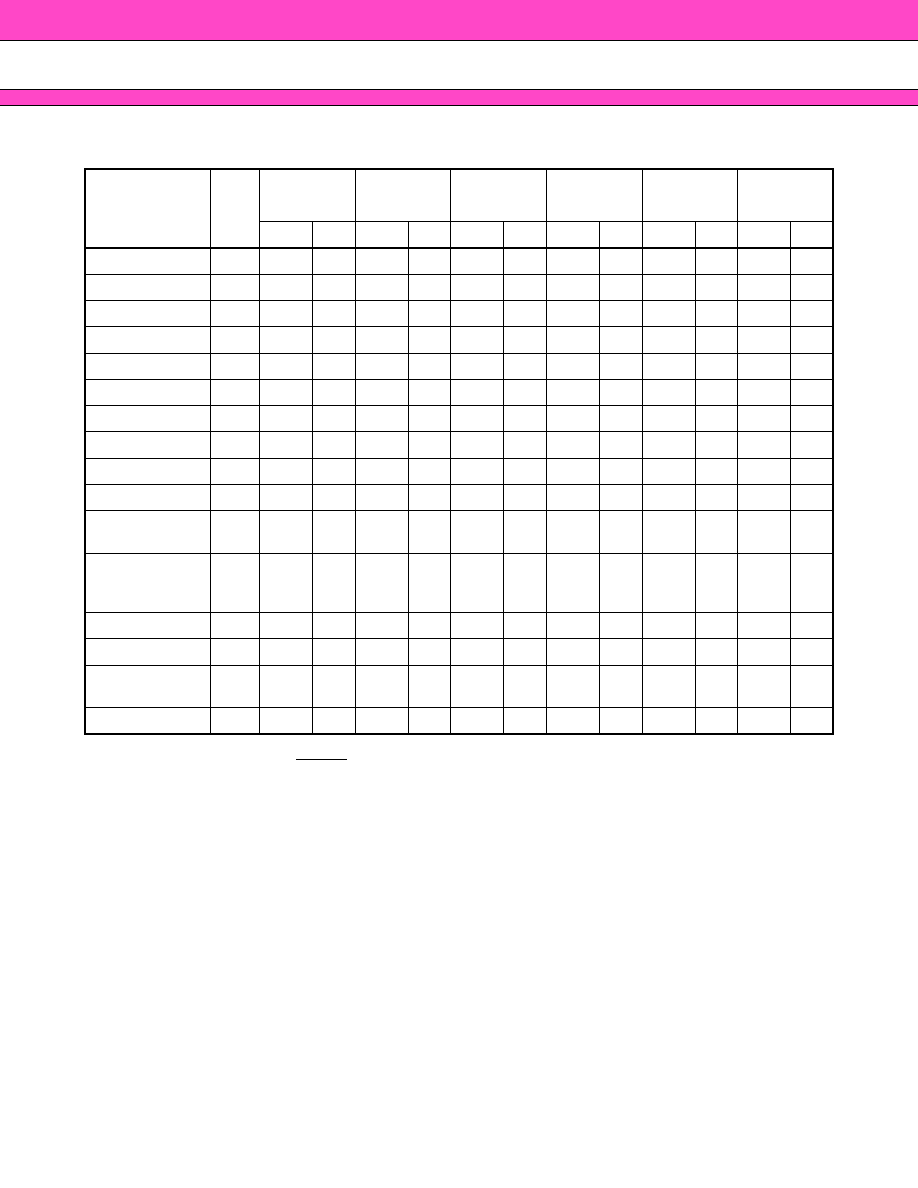
Table 5 Sector Address Tables
Sector
Address
A
21
A
20
A
19
A
18
A
17
A
16
A
15
Sector Size
Address Range
SA0
0
0
0
0
0
0
0
32K words
000000h to 007FFFh
SA1
0
0
0
0
0
0
1
32K words
008000h to 00FFFFh
SA2
0
0
0
0
0
1
0
32K words
010000h to 017FFFh
SA3
0
0
0
0
0
1
1
32K words
018000h to 01FFFFh
SA4
0
0
0
0
1
0
0
32K words
020000h to 027FFFh
SA5
0
0
0
0
1
0
1
32K words
028000h to 02FFFFh
SA6
0
0
0
0
1
1
0
32K words
030000h to 037FFFh
SA7
0
0
0
0
1
1
1
32K words
038000h to 03FFFFh
SA8
0
0
0
1
0
0
0
32K words
040000h to 047FFFh
SA9
0
0
0
1
0
0
1
32K words
048000h to 04FFFFh
SA10
0
0
0
1
0
1
0
32K words
050000h to 057FFFh
SA11
0
0
0
1
0
1
1
32K words
058000h to 05FFFFh
SA12
0
0
0
1
1
0
0
32K words
060000h to 067FFFh
SA13
0
0
0
1
1
0
1
32K words
068000h to 06FFFFh
SA14
0
0
0
1
1
1
0
32K words
070000h to 077FFFh
SA15
0
0
0
1
1
1
1
32K words
078000h to 07FFFFh
SA16
0
0
1
0
0
0
0
32K words
080000h to 087FFFh
SA17
0
0
1
0
0
0
1
32K words
088000h to 08FFFFh
SA18
0
0
1
0
0
1
0
32K words
090000h to 097FFFh
SA19
0
0
1
0
0
1
1
32K words
098000h to 09FFFFh
SA20
0
0
1
0
1
0
0
32K words
0A0000h to 0A7FFFh
SA21
0
0
1
0
1
0
1
32K words
0A8000h to 0AFFFFh
SA22
0
0
1
0
1
1
0
32K words
0B0000h to 0B7FFFh
SA23
0
0
1
0
1
1
1
32K words
0B8000h to 0BFFFFh
SA24
0
0
1
1
0
0
0
32K words
0C0000h to 0C7FFFh
SA25
0
0
1
1
0
0
1
32K words
0C8000h to 0CFFFFh
SA26
0
0
1
1
0
1
0
32K words
0D0000h to 0D7FFFh
SA27
0
0
1
1
0
1
1
32K words
0D8000h to 0DFFFFh
SA28
0
0
1
1
1
0
0
32K words
0E0000h to 0E7FFFh
SA29
0
0
1
1
1
0
1
32K words
0E8000h to 0EFFFFh
SA30
0
0
1
1
1
1
0
32K words
0F0000h to 0F7FFFh
SA31
0
0
1
1
1
1
1
32K words
0F8000h to 0FFFFFh

MBM29LV650UE/651UE-
90/12
12
(Continued)
(Continued)
Sector
Address
A
21
A
20
A
19
A
18
A
17
A
16
A
15
Sector Size
Address Range
SA32
0
1
0
0
0
0
0
32K words
100000h to 107FFFh
SA33
0
1
0
0
0
0
1
32K words
108000h to 10FFFFh
SA34
0
1
0
0
0
1
0
32K words
110000h to 117FFFh
SA35
0
1
0
0
0
1
1
32K words
118000h to 11FFFFh
SA36
0
1
0
0
1
0
0
32K words
120000h to 127FFFh
SA37
0
1
0
0
1
0
1
32K words
128000h to 12FFFFh
SA38
0
1
0
0
1
1
0
32K words
130000h to 137FFFh
SA39
0
1
0
0
1
1
1
32K words
138000h to 13FFFFh
SA40
0
1
0
1
0
0
0
32K words
140000h to 147FFFh
SA41
0
1
0
1
0
0
1
32K words
148000h to 14FFFFh
SA42
0
1
0
1
0
1
0
32K words
150000h to 157FFFh
SA43
0
1
0
1
0
1
1
32K words
158000h to 15FFFFh
SA44
0
1
0
1
1
0
0
32K words
160000h to 167FFFh
SA45
0
1
0
1
1
0
1
32K words
168000h to 16FFFFh
SA46
0
1
0
1
1
1
0
32K words
170000h to 177FFFh
SA47
0
1
0
1
1
1
1
32K words
178000h to 17FFFFh
SA48
0
1
1
0
0
0
0
32K words
180000h to 187FFFh
SA49
0
1
1
0
0
0
1
32K words
188000h to 18FFFFh
SA50
0
1
1
0
0
1
0
32K words
190000h to 197FFFh
SA51
0
1
1
0
0
1
1
32K words
198000h to 19FFFFh
SA52
0
1
1
0
1
0
0
32K words
1A0000h to 1A7FFFh
SA53
0
1
1
0
1
0
1
32K words
1A8000h to 1AFFFFh
SA54
0
1
1
0
1
1
0
32K words
1B0000h to 1B7FFFh
SA55
0
1
1
0
1
1
1
32K words
1B8000h to 1BFFFFh
SA56
0
1
1
1
0
0
0
32K words
1C0000h to 1C7FFFh
SA57
0
1
1
1
0
0
1
32K words
1C8000h to 1CFFFFh
SA58
0
1
1
1
0
1
0
32K words
1D0000h to 1D7FFFh
SA59
0
1
1
1
0
1
1
32K words
1D8000h to 1DFFFFh
SA60
0
1
1
1
1
0
0
32K words
1E0000h to 1E7FFFh
SA61
0
1
1
1
1
0
1
32K words
1E8000h to 1EFFFFh
SA62
0
1
1
1
1
1
0
32K words
1F0000h to 1F7FFFh
SA63
0
1
1
1
1
1
1
32K words
1F8000h to 1FFFFFh

MBM29LV650UE/651UE-
90/12
13
(Continued)
(Continued)
Sector
Address
A
21
A
20
A
19
A
18
A
17
A
16
A
15
Sector Size
Address Range
SA64
1
0
0
0
0
0
0
32K words
200000h to 207FFFh
SA65
1
0
0
0
0
0
1
32K words
208000h to 20FFFFh
SA66
1
0
0
0
0
1
0
32K words
210000h to 217FFFh
SA67
1
0
0
0
0
1
1
32K words
218000h to 21FFFFh
SA68
1
0
0
0
1
0
0
32K words
220000h to 227FFFh
SA69
1
0
0
0
1
0
1
32K words
228000h to 22FFFFh
SA70
1
0
0
0
1
1
0
32K words
230000h to 237FFFh
SA71
1
0
0
0
1
1
1
32K words
238000h to 23FFFFh
SA72
1
0
0
1
0
0
0
32K words
240000h to 247FFFh
SA73
1
0
0
1
0
0
1
32K words
248000h to 24FFFFh
SA74
1
0
0
1
0
1
0
32K words
250000h to 257FFFh
SA75
1
0
0
1
0
1
1
32K words
258000h to 25FFFFh
SA76
1
0
0
1
1
0
0
32K words
260000h to 267FFFh
SA77
1
0
0
1
1
0
1
32K words
268000h to 26FFFFh
SA78
1
0
0
1
1
1
0
32K words
270000h to 277FFFh
SA79
1
0
0
1
1
1
1
32K words
278000h to 27FFFFh
SA80
1
0
1
0
0
0
0
32K words
280000h to 287FFFh
SA81
1
0
1
0
0
0
1
32K words
288000h to 28FFFFh
SA82
1
0
1
0
0
1
0
32K words
290000h to 297FFFh
SA83
1
0
1
0
0
1
1
32K words
298000h to 29FFFFh
SA84
1
0
1
0
1
0
0
32K words
2A0000h to 2A7FFFh
SA85
1
0
1
0
1
0
1
32K words
2A8000h to 2AFFFFh
SA86
1
0
1
0
1
1
0
32K words
2B0000h to 2B7FFFh
SA87
1
0
1
0
1
1
1
32K words
2B8000h to 2BFFFFh
SA88
1
0
1
1
0
0
0
32K words
2C0000h to 2C7FFFh
SA89
1
0
1
1
0
0
1
32K words
2C8000h to 2CFFFFh
SA90
1
0
1
1
0
1
0
32K words
2D0000h to 2D7FFFh
SA91
1
0
1
1
0
1
1
32K words
2D8000h to 2DFFFFh
SA92
1
0
1
1
1
0
0
32K words
2E0000h to 2E7FFFh
SA93
1
0
1
1
1
0
1
32K words
2E8000h to 2EFFFFh
SA94
1
0
1
1
1
1
0
32K words
2F0000h to 2F7FFFh
SA95
1
0
1
1
1
1
1
32K words
2F8000h to 2FFFFFh

MBM29LV650UE/651UE-
90/12
14
(Continued)
Sector
Address
A
21
A
20
A
19
A
18
A
17
A
16
A
15
Sector Size
Address Range
SA96
1
1
0
0
0
0
0
32K words
300000h to 307FFFh
SA97
1
1
0
0
0
0
1
32K words
308000h to 30FFFFh
SA98
1
1
0
0
0
1
0
32K words
310000h to 317FFFh
SA99
1
1
0
0
0
1
1
32K words
318000h to 31FFFFh
SA100
1
1
0
0
1
0
0
32K words
320000h to 327FFFh
SA101
1
1
0
0
1
0
1
32K words
328000h to 32FFFFh
SA102
1
1
0
0
1
1
0
32K words
330000h to 337FFFh
SA103
1
1
0
0
1
1
1
32K words
338000h to 33FFFFh
SA104
1
1
0
1
0
0
0
32K words
340000h to 347FFFh
SA105
1
1
0
1
0
0
1
32K words
348000h to 34FFFFh
SA106
1
1
0
1
0
1
0
32K words
350000h to 357FFFh
SA107
1
1
0
1
0
1
1
32K words
358000h to 35FFFFh
SA108
1
1
0
1
1
0
0
32K words
360000h to 367FFFh
SA109
1
1
0
1
1
0
1
32K words
368000h to 36FFFFh
SA110
1
1
0
1
1
1
0
32K words
370000h to 377FFFh
SA111
1
1
0
1
1
1
1
32K words
378000h to 37FFFFh
SA112
1
1
1
0
0
0
0
32K words
380000h to 387FFFh
SA113
1
1
1
0
0
0
1
32K words
388000h to 38FFFFh
SA114
1
1
1
0
0
1
0
32K words
390000h to 397FFFh
SA115
1
1
1
0
0
1
1
32K words
398000h to 39FFFFh
SA116
1
1
1
0
1
0
0
32K words
3A0000h to 3A7FFFh
SA117
1
1
1
0
1
0
1
32K words
3A8000h to 3AFFFFh
SA118
1
1
1
0
1
1
0
32K words
3B0000h to 3B7FFFh
SA119
1
1
1
0
1
1
1
32K words
3B8000h to 3BFFFFh
SA120
1
1
1
1
0
0
0
32K words
3C0000h to 3C7FFFh
SA121
1
1
1
1
0
0
1
32K words
3C8000h to 3CFFFFh
SA122
1
1
1
1
0
1
0
32K words
3D0000h to 3D7FFFh
SA123
1
1
1
1
0
1
1
32K words
3D8000h to 3DFFFFh
SA124
1
1
1
1
1
0
0
32K words
3E0000h to 3E7FFFh
SA125
1
1
1
1
1
0
1
32K words
3E8000h to 3EFFFFh
SA126
1
1
1
1
1
1
0
32K words
3F0000h to 3F7FFFh
SA127
1
1
1
1
1
1
1
32K words
3F8000h to 3FFFFFh

MBM29LV650UE/651UE-
90/12
15
Table 6 Sector Group Address
Sector Group
Address
A
21
A
20
A
19
A
18
A
17
Sector Group Size
Sectors
SGA0
0
0
0
0
0
128K words
SA0 to SA3
SGA1
0
0
0
0
1
128K words
SA4 to SA7
SGA2
0
0
0
1
0
128K words
SA8 to SA11
SGA3
0
0
0
1
1
128K words
SA12 to SA15
SGA4
0
0
1
0
0
128K words
SA16 to SA19
SGA5
0
0
1
0
1
128K words
SA20 to SA23
SGA6
0
0
1
1
0
128K words
SA24 to SA27
SGA7
0
0
1
1
1
128K words
SA28 to SA31
SGA8
0
1
0
0
0
128K words
SA32 to SA35
SGA9
0
1
0
0
1
128K words
SA36 to SA39
SGA10
0
1
0
1
0
128K words
SA40 to SA43
SGA11
0
1
0
1
1
128K words
SA44 to SA47
SGA12
0
1
1
0
0
128K words
SA48 to SA51
SGA13
0
1
1
0
1
128K words
SA52 to SA55
SGA14
0
1
1
1
0
128K words
SA56 to SA59
SGA15
0
1
1
1
1
128K words
SA60 to SA63
SGA16
1
0
0
0
0
128K words
SA64 to SA67
SGA17
1
0
0
0
1
128K words
SA68 to SA71
SGA18
1
0
0
1
0
128K words
SA72 to SA75
SGA19
1
0
0
1
1
128K words
SA76 to SA79
SGA20
1
0
1
0
0
128K words
SA80 to SA83
SGA21
1
0
1
0
1
128K words
SA84 to SA87
SGA22
1
0
1
1
0
128K words
SA88 to SA91
SGA23
1
0
1
1
1
128K words
SA92 to SA95
SGA24
1
1
0
0
0
128K words
SA96 to SA99
SGA25
1
1
0
0
1
128K words
SA100 to SA103
SGA26
1
1
0
1
0
128K words
SA104 to SA107
SGA27
1
1
0
1
1
128K words
SA108 to SA111
SGA28
1
1
1
0
0
128K words
SA112 to SA115
SGA29
1
1
1
0
1
128K words
SA116 to SA119
SGA30
1
1
1
1
0
128K words
SA120 to SA123
SGA31
1
1
1
1
1
128K words
SA124 to SA127

MBM29LV650UE/651UE-
90/12
16
Table 7 Common Flash Memory Interface Code
Description
A
0
to A
6
DQ
0
to DQ
15
Query-unique ASCII string
"QRY"
10h
11h
12h
0051h
0052h
0059h
Primary OEM Command Set
2h: AMD/FJ standard type
13h
14h
0002h
0000h
Address for Primary
Extended Table
15h
16h
0040h
0000h
Alternate OEM Command
Set (00h = not applicable)
17h
18h
0000h
0000h
Address for Alternate OEM
Extended Table
19h
1Ah
0000h
0000h
V
CC
Min. (write/erase)
D7-4: volt, D3-0: 100 mvolt
1Bh
0027h
V
CC
Max. (write/erase)
D7-4: volt, D3-0: 100 mvolt
1Ch
0036h
V
PP
Min. voltage
1Dh
0000h
V
PP
Max. voltage
1Eh
0000h
Typical timeout per single
byte/word write 2
N
µ
s
1Fh
0004h
Typical timeout for Min. size
buffer write 2
N
µ
s
20h
0000h
Typical timeout per individual
block erase 2
N
ms
21h
000Ah
Typical timeout for full chip
erase 2
N
ms
22h
0000h
Max. timeout for byte/word
write 2
N
times typical
23h
0005h
Max. timeout for buffer write
2
N
times typical
24h
0000h
Max. timeout per individual
block erase 2
N
times typical
25h
0004h
Max. timeout for full chip
erase 2
N
times typical
26h
0000h
Device Size = 2
N
byte
27h
0017h
Flash Device Interface
description
28h
29h
0001h
0000h
Max. number of byte in
multi-byte write = 2
N
2Ah
2Bh
0000h
0000h
Number of Erase Block
Regions within device
2Ch
0001h
Erase Block Region 1
Information
2Dh
2Eh
2Fh
30h
007Fh
0000h
0000h
0001h
Description
A
0
to A
6
DQ
0
to DQ
15
Erase Block Region 2
Information
31h
32h
33h
34h
0000h
0000h
0000h
0000h
Query-unique ASCII string
"PRI"
40h
41h
42h
0050h
0052h
0049h
Major version number, ASCII
43h
0031h
Minor version number, ASCII
44h
0031h
Address Sensitive Unlock
0h = Required
1h = Not Required
45h
0001h
Erase Suspend
0h = Not Supported
1h = To Read Only
2h = To Read & Write
46h
0002h
Sector Protection
0h = Not Supported
X = Number of sectors in per
group
47h
0004h
Sector Temporary
Unprotection
00h = Not Supported
01h = Supported
48h
0001h
Sector Protection Algorithm
49h
0004h
Number of Sector for Bank 2
00h = Not Supported
4Ah
0000h
Burst Mode Type
00h = Not Supported
4Bh
0000h
Page Mode Type
00h = Not Supported
4Ch
0000h
ACC (Acceleration) Supply
Minimum
00h = Not Supported,
D7-4: volt, D3-0: 100 mvolt
4Dh
00B5h
ACC (Acceleration) Supply
Maximum
00h = Not Supported,
D7-4: volt, D3-0: 100 mvolt
4Eh
00C5h
Boot Type
04h = MBM29LV651UE
05h = MBM29LV650UE
4Fh
00XXh

MBM29LV650UE/651UE-
90/12
17
s
s
s
s
FUNCTIONAL DESCRIPTION
Read Mode
The MBM29LV650UE/651UE has two control functions which must be satisfied in order to obtain data at the
outputs. CE is the power control and should be used for a device selection. OE is the output control and should
be used to gate data to the output pins if a device is selected.
Address access time (t
ACC
) is equal to the delay from stable addresses to valid output data. The chip enable
access time (t
CE
) is the delay from stable addresses and stable CE to valid data at the output pins. The output
enable access time is the delay from the falling edge of OE to valid data at the output pins. (Assuming the
addresses have been stable for at least t
ACC
-t
OE
time.) When reading out a data without changing addresses after
power-up, it is necessary to input hardware reset or to change CE pin from "H" or "L".
Standby Mode
There are two ways to implement the standby mode on the MBM29LV650UE/651UE devices, one using both
the CE and RESET pins; the other via the RESET pin only.
When using both pins, a CMOS standby mode is achieved with CE and RESET inputs both held at V
CC
±0.3 V.
Under this condition the current consumed is less than 5
µ
A max. During Embedded Algorithm operation, V
CC
active current (I
CC2
) is required even CE = "H". The device can be read with standard access time (t
CE
) from either
of these standby modes.
When using the RESET pin only, a CMOS standby mode is achieved with RESET input held at V
SS
±0.3 V (CE
= "H" or "L"). Under this condition the current consumed is less than 5
µ
A max. Once the RESET pin is taken
high, the device requires t
RH
of wake up time before outputs are valid for read access.
In the standby mode the outputs are in the high impedance state, independent of the OE input.
Automatic Sleep Mode
There is a function called automatic sleep mode to restrain power consumption during read-out of
MBM29LV650UE/651UE data. This mode can be used effectively with an application requesting low power
consumption such as handy terminals.
To activate this mode, MBM29LV650UE/651UE automatically switch themselves to low power mode when
MBM29LV650UE/651UE addresses remain stable during access fine of 150 ns. It is not necessary to control
CE, WE, and OE on the mode. Under the mode, the current consumed is typically 1
µ
A (CMOS Level).
Since the data are latched during this mode, the data are read-out continuously. If the addresses are changed,
the mode is canceled automatically and MBM29LV650UE/651UE read-out the data for changed addresses.
Output Disable
With the OE input at a logic high level (V
IH
), output from the devices are disabled. This will cause the output pins
to be in a high impedance state.
Autoselect
The autoselect mode allows the reading out of a binary code from the devices and will identify its manufacturer
and type. This mode is intended for use by programming equipment for the purpose of automatically matching
the devices to be programmed with its corresponding programming algorithm. The Autoselect command may
also be used to check the status of write-protected sectors (see Tables 4.1 and 4.2). This mode is functional
over the entire temperature range of the devices.
To activate this mode, the programming equipment must force V
ID
(11.5 V to 12.5 V) on address pin A
9
. Two
identifier bytes may then be sequenced from the devices outputs by toggling address A
0
from V
IL
to V
IH
. All
addresses are DON'T CARES except A
0
, A
1
, and A
6
. (See Table 2.)
The manufacturer and device codes may also be read via the command register, for instances when the
MBM29LV650UE/651UE is erased or programmed in a system without access to high voltage on the A
9
pin.
The command sequence is illustrated in Table 3. (Refer to Autoselect Command section.)

MBM29LV650UE/651UE-
90/12
18
Word 0 (A
0
= V
IL
) represents the manufacturer's code (Fujitsu = 04h) and word 1 (A
0
= V
IH
) represents the device
identifier code (MBM29LV650UE/651UE = 22D7h). Word 3 (A
0
= A
1
= V
IH
) represents the Extended Code
(MBM29LV650UE = 2201h, MBM29LV651UE = 2200h). These three words are given in the tables 4.1 to 4.2.
All identifiers for manufactures and device will exhibit odd parity with DQ
7
defined as the parity bit. In order to
read the proper device codes when executing the autoselect, A
1
must be V
IL
. (See Tables 4.1 to 4.2.)
In order to determine which sectors are write protected, A
1
must be at V
IH
while running through the sector
addresses; if the selected sector is protected, a logical `1' will be output on DQ
0
(DQ
0
= 1).
Write
Device erasure and programming are accomplished via the command register. The contents of the register serve
as inputs to the internal state machine. The state machine outputs dictate the function of the device.
The command register itself does not occupy any addressable memory location. The register is a latch used to
store the commands, along with the address and data information needed to execute the command. The
command register is written by bringing WE to V
IL
, while CE is at V
IL
and OE is at V
IH
. Addresses are latched on
the falling edge of WE or CE, whichever happens later; while data is latched on the rising edge of WE or CE,
whichever happens first. Standard microprocessor write timings are used.
Refer to AC Write Characteristics and the Erase/Programming Waveforms for specific timing parameters.
Sector Group Protection
The MBM29LV650UE/651UE features hardware sector group protection. This feature will disable both program
and erase operations in any combination of twenty five sector groups of memory. (See Table 6). The sector
group protection feature is enabled using programming equipment at the user's site. The device is shipped with
all sector groups unprotected.
To activate this mode, the programming equipment must force V
ID
on address pin A
9
and control pin OE, (suggest
V
ID
= 11.5 V), CE = V
IL
and A
0
= A
6
= V
IL
, A
1
= V
IH
. The sector group addresses (A
21
, A
20
, A
19
, A
18
, and A
17
) should
be set to the sector to be protected. Table 5 defines the sector address for each of the one hundred twenty-eight
(128) individual sectors, and tables 2 defines the sector group address for each of the thirty-two (32) individual
group sectors. Programming of the protection circuitry begins on the falling edge of the WE pulse and is
terminated with the rising edge of the same. Sector group addresses must be held constant during the WE pulse.
See figures 12 and 20 for sector group protection waveforms and algorithm.
To verify programming of the protection circuitry, the programming equipment must force V
ID
on address pin A
9
with CE and OE at V
IL
and WE at V
IH
. Scanning the sector group addresses (A
21
, A
20
, A
19
, A
18
, and A
17
) while
(A
6
, A
1
, A
0
) = (0, 1, 0) will produce a logical "1" code at device output DQ
0
for a protected sector. Otherwise the
device will produce "0" for unprotected sector. In this mode, the lower order addresses, except for A
0
, A
1
, and
A
6
are DON'T CARES. Address locations with A
1
= V
IL
are reserved for Autoselect manufacturer and device codes.
It is also possible to determine if a sector group is protected in the system by writing an Autoselect command.
Performing a read operation at the address location XX02h, where the higher order addresses (A
21
, A
20
, A
19
, A
18
,
and A
17
) are the desired sector group address will produce a logical "1" at DQ
0
for a protected sector group. See
Tables 4.1 and 4.2 for Autoselect codes.
Temporary Sector Group Unprotection
This feature allows temporary unprotection of previously protected sector groups of the MBM29LV650UE/651UE
devices in order to change data. The Sector Group Unprotection mode is activated by setting the RESET pin to
high voltage (V
ID
). During this mode, formerly protected sector groups can be programmed or erased by selecting
the sector group addresses. Once the V
ID
is taken away from the RESET pin, all the previously protected sector
groups will be protected again. Refer to Figures 13 and 21.
This temporary sector group unprotect mode is disabled whenever the chip is in the Hidden ROM (Hi-ROM)
mode. This area can not be programmed within this mode. Moreover once this area is programmed, it is always
protected no matter in which mode.

MBM29LV650UE/651UE-
90/12
19
RESET
Hardware Reset Pin
The MBM29LV650UE/651UE devices may be reset by driving the RESET pin to V
IL
. The RESET pin has a pulse
requirement and has to be kept low (V
IL
) for at least "t
RP
" in order to properly reset the internal state machine.
Any operation in the process of being executed will be terminated and the internal state machine will be reset
to the read mode "t
READY
" after the RESET pin is driven low. Furthermore, once the RESET pin goes high, the
devices require an additional "t
RH
" before it will allow read access. When the RESET pin is low, the devices will
be in the standby mode for the duration of the pulse and all the data output pins will be tri-stated. If a hardware
reset occurs during a program or erase operation, the data at that particular location will be corrupted.
Write Protect (WP)
The Write Protection function provides a hardware method of protecting certain "outermost" 32K word sector
without using V
ID
.
If the system asserts V
IL
on the WP pin, the device disables program and erase functions in the "outermost"
32K word sector independently of whether this sector was protected or unprotected using the method described
in "Sector Protection/Unprotection". The outermost 32K word sector is the highest addresses in
MBM29LV650UE, or the lowest addresses in MBM29LV651UE.
(MBM29LV650UE: SA127, MBM29LV651UE: SA0)
If the system asserts V
IH
on the WP pin, the device reverts to whether the outermost 32K word sector was last
set to be protected or unprotected. That is, sector protection or unprotection for this sector depends on whether
this was last protected or unprotected using the method described in "Sector protection/unprotection".
Accelerated Program Operation
MBM29LV650UE/651UE offers accelerated program operation which enables the programming in high speed.
If the system asserts V
ACC
to the ACC pin, the device automatically enters the acceleration mode and the time
required for program operation will reduce to about 50%. This function is primarily intended to allow high speed
program, so caution is needed as the sector group will temporarily be unprotected.
The system would use a fast program command sequence when programming during acceleration mode. Set
command to fast mode and reset command from fast mode is not necessary. When the device enters the
acceleration mode, the device automatically set to fast mode. Therefore, the present sequence could be used
for programming and detection of completion during acceleration mode.
Removing V
ACC
from the ACC pin returns the device to normal operation. Do not remove V
ACC
from the ACC pin
while programming. (See Figure 15.)

MBM29LV650UE/651UE-
90/12
20
s
s
s
s
COMMAND DEFINITIONS
Device operations are selected by writing specific address and data sequences into the command register.
Writing incorrect data values or writing them in the improper sequence will reset the devices to the read mode.
Table 3 defines the valid register command sequences. Note that the Erase Suspend (B0h) and Erase Resume
(30h) commands are valid only while the Sector Erase operation is in progress. Moreover both Read/Reset
commands are functionally equivalent, resetting the device to the read mode. Please note that commands are
always written at DQ
0
to DQ
7
and DQ
8
to DQ
15
bits are ignored.
Read/Reset Command
In order to return from Autoselect mode or Exceeded Timing Limits (DQ
5
= 1) to Read/Reset mode, the Read/
Reset operation is initiated by writing the Read/Reset command sequence into the command register.
Microprocessor read cycles retrieve array data from the memory. The devices remain enabled for reads until the
command register contents are altered.
The devices will automatically power-up in the Read/Reset state. In this case, a command sequence is not
required to read data. Standard microprocessor read cycles will retrieve array data. This default value ensures
that no spurious alteration of the memory content occurs during the power transition. Refer to the AC Read
Characteristics and Waveforms for the specific timing parameters.
Autoselect Command
Flash memories are intended for use in applications where the local CPU alters memory contents. As such,
manufacture and device codes must be accessible while the devices reside in the target system. PROM
programmers typically access the signature codes by raising A
9
to a high voltage. However, multiplexing high
voltage onto the address lines is not generally desired system design practice.
The device contains an Autoselect command operation to supplement traditional PROM programming
methodology. The operation is initiated by writing the Autoselect command sequence into the command register.
The Autoselect command sequence is initiated by first writing two unlock cycles. This is followed by a third write
cycle that contains the address and the Autoselect command. Then the manufacture and device codes can be
read from the address, and an actual data of memory cell can be read from the another address.
Following the command write, a read cycle from address XX00h retrieves the manufacture code of 04h. A read
cycle from address XX01h returns the device code (MBM29LV650UE/651UE = 22D7h). A read cycle from
address XX03h returns the Extended Code (MBM29LV650UE = 0010h, MBM29LV651UE = 0000h). (See Tables
4.1 and 4.2.)
All manufacturer and device codes will exhibit odd parity with DQ
7
defined as the parity bit. Sector state (protection
or unprotection) will be informed by address XX02h. Scanning the sector group addresses (A
21
, A
20
, A
19
, A
18
,
and A
17
) while (A
6
, A
1
, A
0
) = (0, 1, 0) will produce a logical "1" at device output DQ
0
for a protected sector group.
The programming verification should be performed by verify sector group protection on the protected sector.
(See Table 2.)
To terminate the operation, it is necessary to write the Read/Reset command sequence into the register, and
also to write the Autoselect command during the operation, execute it after writing Read/Reset command
sequence.

MBM29LV650UE/651UE-
90/12
21
Word Programming
The devices are programmed on a word-by-word basis. Programming is a four bus cycle operation. There are
two "unlock" write cycles. These are followed by the program set-up command and data write cycles. Addresses
are latched on the falling edge of CE or WE, whichever happens later and the data is latched on the rising edge
of CE or WE, whichever happens first. The rising edge of CE or WE (whichever happens first) begins
programming. Upon executing the Embedded Program Algorithm command sequence, the system is not required
to provide further controls or timings. The device will automatically provide adequate internally generated
program pulses and verify the programmed cell margin.
The system can determine the status of the program operation by using DQ
7
(Data Polling), and DQ
6
(Toggle
Bit). The Data Polling and Toggle Bit must be performed at the memory location which is being programmed.
The automatic programming operation is completed when the data on DQ
7
is equivalent to data written to this
bit at which time the devices return to the read mode and addresses are no longer latched. (See Table 8, Hardware
Sequence Flags.) Therefore, the devices require that a valid address to the devices be supplied by the system
at this particular instance of time. Hence, Data Polling must be performed at the memory location which is being
programmed.
Any commands written to the chip during this period will be ignored. If hardware reset occurs during the
programming operation, it is impossible to guarantee the data are being written.
Programming is allowed in any sequence and across sector boundaries. Beware that a data "0" cannot be
programmed back to a "1" Attempting to do so may either hang up the device or result in an apparent success
according to the data polling algorithm but a read from Read/Reset mode will show that the data is still "0" Only
erase operations can convert "0"s to "1"s.
Figure 16 illustrates the Embedded Program
TM
Algorithm using typical command strings and bus operations.
Chip Erase
Chip erase is a six bus cycle operation. There are two "unlock" write cycles. These are followed by writing the
"set-up" command. Two more "unlock" write cycles are then followed by the chip erase command.
Chip erase does not require the user to program the device prior to erase. Upon executing the Embedded Erase
Algorithm command sequence the devices will automatically program and verify the entire memory for an all
zero data pattern prior to electrical erase (Preprogram function). The system is not required to provide any
controls or timings during these operations.
The system can determine the status of the erase operation by using DQ
7
(Data Polling), and DQ
6
(Toggle Bit).
The chip erase begins on the rising edge of the last CE or WE, whichever happens first in the command sequence
and terminates when the data on DQ
7
is "1" (See Write Operation Status section.) at which time the device
returns to read the mode.
Chip Erase Time; Sector Erase Time
◊
All sectors + Chip Program Time (Preprogramming)
Figure 17 illustrates the Embedded Erase
TM
Algorithm using typical command strings and bus operations.
Sector Erase
Sector erase is a six bus cycle operation. There are two "unlock" write cycles. These are followed by writing the
"set-up" command. Two more "unlock" write cycles are then followed by the Sector Erase command. The sector
address (any address location within the desired sector) is latched on the falling edge of CE or WE whichever
happens later, while the command (Data = 30h) is latched on the rising edge of CE or WE which happens first.
After time-out of "t
TOW
" from the rising edge of the last sector erase command, the sector erase operation will begin.

MBM29LV650UE/651UE-
90/12
22
Multiple sectors may be erased concurrently by writing the six bus cycle operations on Table 3. This sequence
is followed with writes of the Sector Erase command to addresses in other sectors desired to be concurrently
erased. The time between writes must be less than "t
TOW
" otherwise that command will not be accepted and
erasure will start. It is recommended that processor interrupts be disabled during this time to guarantee this
condition. The interrupts can be re-enabled after the last Sector Erase command is written. A time-out of "t
TOW
"
from the rising edge of last CE or WE whichever happens first will initiate the execution of the Sector Erase
command(s). If another falling edge of CE or WE, whichever happens first occurs within the "t
TOW
" time-out
window the timer is reset. (Monitor DQ
3
to determine if the sector erase timer window is still open, see section
DQ
3
, Sector Erase Timer.) Any command other than Sector Erase or Erase Suspend during this time-out period
will reset the devices to the read mode, ignoring the previous command string. Resetting the devices once
execution has begun will corrupt the data in the sector. In that case, restart the erase on those sectors and allow
them to complete. (Refer to the Write Operation Status section for Sector Erase Timer operation.) Loading the
sector erase buffer may be done in any sequence and with any number of sectors (0 to 127).
Sector erase does not require the user to program the devices prior to erase. The devices automatically program
all memory locations in the sector(s) to be erased prior to electrical erase (Preprogram function). When erasing
a sector or sectors the remaining unselected sectors are not affected. The system is not required to provide any
controls or timings during these operations.
The system can determine the status of the erase operation by using DQ
7
(Data Polling), and DQ
6
(Toggle Bit).
The sector erase begins after the "t
TOW
" time out from the rising edge of CE or WE whichever happens first for
the last sector erase command pulse and terminates when the data on DQ
7
is "1" (See Write Operation Status
section.) at which time the devices return to the read mode. Data polling and Toggle Bit must be performed at
an address within any of the sectors being erased.
Multiple Sector Erase Time; [Sector Erase Time + Sector Program Time (Preprogramming)]
◊
Number of Sector
Erase
Figure 17 illustrates the Embedded Erase
TM
Algorithm using typical command strings and bus operations.
Erase Suspend/Resume
The Erase Suspend command allows the user to interrupt a Sector Erase operation and then perform data reads
from or programs to a sector not being erased. This command is applicable ONLY during the Sector Erase
operation which includes the time-out period for sector erase. The Erase Suspend command will be ignored if
written during the Chip Erase operation or Embedded Program Algorithm. Writting the Erase Suspend command
(B0h) during the Sector Erase time-out results in immediate termination of the time-out period and suspension
of the erase operation.
Writing the Erase Resume command (30h) resumes the erase operation. The addresses are "Don't Care" when
writting the Erase Suspend or Erase Resume command.
When the Erase Suspend command is written during the Sector Erase operation, the device will take a maximum
of "t
SPD
" to suspend the erase operation. When the devices have entered the erase-suspended mode, the DQ
7
bit will be at logic "1" and DQ
6
will stop toggling. The user must use the address of the erasing sector for reading
DQ
6
and DQ
7
to determine if the erase operation has been suspended. Further writes of the Erase Suspend
command are ignored.
When the erase operation has been suspended, the devices default to the erase-suspend-read mode. Reading
data in this mode is the same as reading from the standard read mode except that the data must be read from
sectors that have not been erase-suspended. Successively reading from the erase-suspended sector while the
device is in the erase-suspend-read mode will cause DQ
2
to toggle. (See the section on DQ
2
.)

MBM29LV650UE/651UE-
90/12
23
After entering the erase-suspend-read mode, the user can program the device by writing the appropriate
command sequence for Program. This program mode is known as the erase-suspend-program mode. Again,
programming in this mode is the same as programming in the regular Program mode except that the data must
be programmed to sectors that are not erase-suspended. Successively reading from the erase-suspended sector
while the devices are in the erase-suspend-program mode will cause DQ
2
to toggle. The end of the erase-
suspended Program operation is detected by the Data polling of DQ
7
or by the Toggle Bit I (DQ
6
) which is the
same as the regular Program operation. Note that DQ
7
must be read from the Program address while DQ
6
can
be read from any address.
To resume the operation of Sector Erase, the Resume command (30h) should be written. Any further writes of
the Resume command at this point will be ignored. Another Erase Suspend command can be written after the
chip has resumed erasing.
Extended Command
(1) Fast Mode
MBM29LV650UE/651UE has Fast Mode function. This mode dispenses with the initial two unclock cycles
required in the standard program command sequence by writing Fast Mode command into the command register.
In this mode, the required bus cycle for programming is two cycles instead of four bus cycles in standard program
command. (Do not write erase command in this mode.) The read operation is also executed after exiting this
mode. To exit this mode, it is necessary to write Fast Mode Reset command into the command register. (Refer
to the Figure 22.) The V
CC
active current is required even CE = V
IH
during Fast Mode.
(2) Fast Programming
During Fast Mode, the programming can be executed with two bus cycles operation. The Embedded Program
Algorithm is executed by writing program set-up command (A0h) and data write cycles (PA/PD). (Refer to the
Figure 22.)
(3) Extended Sector Group Protection
In addition to normal sector group protection, the MBM29LV650UE/651UE has Extended Sector Group
Protection as extended function. This function enable to protect sector group by forcing V
ID
on RESET pin and
write a command sequence. Unlike conventional procedure, it is not necessary to force V
ID
and control timing
for control pins. The only RESET pin requires V
ID
for sector group protection in this mode. The extended sector
group protection requires V
ID
on RESET pin. With this condition, the operation is initiated by writing the set-up
command (60h) into the command register. Then, the sector group addresses pins (A
21
, A
20
, A
19
, A
18
, and A
17
)
and (A
6
, A
1
, A
0
) = (0, 1, 0) should be set to the sector group to be protected (recommend to set V
IL
for the other
addresses pins), and write extended sector group protection command (60h). A sector group is typically protected
in 250
µ
s. To verify programming of the protection circuitry, the sector group addresses pins (A
21
, A
20
, A
19
, A
18
,
and A
17
) and (A
6
, A
1
, A
0
) = (0, 1, 0) should be set and write a command (40h). Following the command write, a
logical "1" at device output DQ
0
will produce for protected sector in the read operation. If the output data is logical
"0", please repeat to write extended sector group protection command (60h) again. To terminate the operation,
it is necessary to set RESET pin to V
IH
. (Refer to the Figures 14 and 23.)
(4) CFI (Common Flash Memory Interface)
The CFI (Common Flash Memory Interface) specification outlines device and host system software interrogation
handshake which allows specific vendor-specified software algorithms to be used for entire families of devices.
This allows device-independent, JEDEC ID-independent, and forward-and backward-compatible software
support for the specified flash device families. Refer to CFI specification in detail.
The operation is initiated by writing the query command (98h) into the command register. Following the command
write, a read cycle from specific address retrieves device information. Please note that output data of upper byte
(DQ
8
to DQ
15
) is "0" in word mode (16 bit) read. Refer to the CFI code table. To terminate operation, it is necessary
to write the read/reset command sequence into the register. (See Table 7.)

MBM29LV650UE/651UE-
90/12
24
Hidden ROM (Hi-ROM) Region
The Hi-ROM feature provides a Flash memory region that the system may access through a new command
sequence. This is primarily intended for customers who wish to use an Electronic Serial Number (ESN) in the
device with the ESN protected against modification. Once the Hi-ROM region is programmed, any further
modification of that region is impossible. This ensures the security of the ESN once the product is shipped to
the field.
The Hi-ROM region is 128 words in length. After the system has written the Enter Hi-ROM command sequence,
it may read the Hidden ROM region by using device addresses A
0
to A
6
(A
7
to A
14
are "00", A
15
to A
21
are don't
care). That is, the device sends only program command that would normally be sent to the address to the Hi-
ROM region. This mode of operation continues until the system issues the Exit Hi-ROM command sequence,
or until power is removed from the device. On power-up, or following a hardware reset, the device reverts to
sending commands to the address.
If you request Fujitsu to program the ESN in the device, please contact a Fujitsu representative for more
information.
Write Operation Status
Detailed in Table 8 are all the status flags that can be used to check the status of the device for current mode
operation. During sector erase, the part provides the status flags automatically to the I/O ports. The information
on DQ
2
is address sensitive. This means that if an address from an erasing sector is consecutively read, then
the DQ
2
bit will toggle. However, DQ
2
will not toggle if an address from a non-erasing sector is consecutively
read. This allows the user to determine which sectors are erasing and which are not.
Once erase suspend is entered, address sensitivity still applies. If the address of a non-erasing sector (that is,
one available for read) is provided, then stored data can be read from the device. If the address of an erasing
sector (that is, one unavailable for read) is applied, the device will output its status bits.
*: Successive reads from the erasing or erase-suspend sector will cause DQ
2
to toggle. Reading from non-erase
suspend sector address will indicate logic "1" at the DQ
2
bit.
Notes: 1. DQ
0
and DQ
1
are reserve pins for future use.
2. DQ
4
is Fujitsu internal use only.
Table 8 Hardware Sequence Flags
Status
DQ
7
DQ
6
DQ
5
DQ
3
DQ
2
In Progress
Embedded Program Algorithm
DQ
7
Toggle
0
0
1
Embedded Erase Algorithm
0
Toggle
0
1
Toggle*
Erase
Suspended
Mode
Erase Suspend Read
(Erase Suspended Sector)
1
1
0
0
Toggle
Erase Suspend Read
(Non-Erase Suspended Sector)
Data
Data
Data
Data
Data
Erase Suspend Program
(Non-Erase Suspended Sector)
DQ
7
Toggle
0
0
1*
Exceeded
Time Limits
Embedded Program Algorithm
DQ
7
Toggle
1
0
1
Embedded Erase Algorithm
0
Toggle
1
1
N/A
Erase
Suspended
Mode
Erase Suspend Program
(Non-Erase Suspended Sector)
DQ
7
Toggle
1
0
N/A

MBM29LV650UE/651UE-
90/12
25
DQ
7
Data Polling
The MBM29LV650UE/651UE devices feature Data Polling as a method to indicate to the host that the Embedded
Algorithms are in progress or completed. During the Embedded Program Algorithm an attempt to read the
devices will produce the complement of the data last written to DQ
7
. Upon completion of the Embedded Program
Algorithm, an attempt to read the device will produce the true data last written to DQ
7
. During the Embedded
Erase Algorithm, an attempt to read the device will produce a "0" at the DQ
7
output. Upon completion of the
Embedded Erase Algorithm an attempt to read the device will produce a "1" at the DQ
7
output. The flowchart
for Data Polling (DQ
7
) is shown in Figure 18.
For programming, the Data Polling is valid after the rising edge of fourth write pulse in the four write pulse
sequence.
For chip erase and sector erase, the Data Polling is valid after the rising edge of the sixth write pulse in the six
write pulse sequence. Data Polling must be performed at sector address within any of the sectors being erased
and not a protected sector. Otherwise, the status may not be valid.
Once the Embedded Algorithm operation is close to being completed, the MBM29LV650UE/651UE data pins
(DQ
7
) may change asynchronously while the output enable (OE) is asserted low. This means that the devices
are driving status information on DQ
7
at one instant of time and then that byte's valid data at the next instant of
time. Depending on when the system samples the DQ
7
output, it may read the status or valid data. Even if the
device has completed the Embedded Algorithm operation and DQ
7
has a valid data, the data outputs on DQ
0
to DQ
6
may be still invalid. The valid data on DQ
0
to DQ
7
will be read on the successive read attempts.
The Data Polling feature is only active during the Embedded Programming Algorithm, Embedded Erase Algorithm
or sector erase time-out. (See Table 8.)
See Figure 9 for the Data Polling timing specifications and diagram.
DQ
6
Toggle Bit I
The MBM29LV650UE/651UE also feature the "Toggle Bit I" as a method to indicate to the host system that the
Embedded Algorithms are in progress or completed.
During an Embedded Program or Erase Algorithm cycle, successive attempts to read (OE toggling) data from
the devices will result in DQ
6
toggling between one and zero. Once the Embedded Program or Erase Algorithm
cycle is completed, DQ
6
will stop toggling and valid data will be read on the next successive attempts. During
programming, the Toggle Bit I is valid after the rising edge of the fourth write pulse in the four write pulse sequence.
For chip erase and sector erase, the Toggle Bit I is valid after the rising edge of the sixth write pulse in the six
write pulse sequence. The Toggle Bit I is active during the sector time out.
In programming, if the sector being written to is protected, the toggle bit will toggle for about 1
µ
s and then stop
toggling without the data having changed. In erase, the devices will erase all the selected sectors except for the
ones that are protected. If all selected sectors are protected, the chip will toggle the toggle bit for about 400
µ
s
and then drop back into read mode, having changed none of the data.
Either CE or OE toggling will cause the DQ
6
to toggle. In addition, an Erase Suspend/Resume command will
cause the DQ
6
to toggle.
See Figure 10 for the Toggle Bit I timing specifications and diagram.

MBM29LV650UE/651UE-
90/12
26
DQ
5
Exceeded Timing Limits
DQ
5
will indicate if the program or erase time has exceeded the specified limits (internal pulse count). Under
these conditions DQ
5
will produce a "1". This is a failure condition which indicates that the program or erase
cycle was not successfully completed. Data Polling is the only operating function of the devices under this
condition. The CE circuit will partially power down the device under these conditions (to approximately 2 mA).
The OE and WE pins will control the output disable functions as described in Table 2.
The DQ
5
failure condition may also appear if a user tries to program a non blank location without erasing. In this
case the devices lock out and never complete the Embedded Algorithm operation. Hence, the system never
reads a valid data on DQ
7
bit and DQ
6
never stops toggling. Once the devices have exceeded timing limits, the
DQ
5
bit will indicate a "1". Please note that this is not a device failure condition since the devices were incorrectly
used. If this occurs, reset the device with command sequence.
DQ
3
Sector Erase Timer
After the completion of the initial sector erase command sequence the sector erase time-out will begin. DQ
3
will
remain low until the time-out is complete. Data Polling and Toggle Bit are valid after the initial sector erase
command sequence.
If Data Polling or the Toggle Bit I indicates the device has been written with a valid erase command, DQ
3
may
be used to determine if the sector erase timer window is still open. If DQ
3
is high ("1") the internally controlled
erase cycle has begun; attempts to write subsequent commands to the device will be ignored until the erase
operation is completed as indicated by Data Polling or Toggle Bit I. If DQ
3
is low ("0"), the device will accept
additional sector erase commands. To insure the command has been accepted, the system software should
check the status of DQ
3
prior to and following each subsequent Sector Erase command. If DQ
3
were high on
the second status check, the command may not have been accepted.
See Table 8 : Hardware Sequence Flags.
DQ
2
Toggle Bit II
This toggle bit II, along with DQ
6
, can be used to determine whether the devices are in the Embedded Erase
Algorithm or in Erase Suspend.
Successive reads from the erasing sector will cause DQ
2
to toggle during the Embedded Erase Algorithm. If the
devices are in the erase-suspended-read mode, successive reads from the erase-suspended sector will cause
DQ
2
to toggle. When the devices are in the erase-suspended-program mode, successive reads from the byte
address of the non-erase suspended sector will indicate a logic "1" at the DQ
2
bit.
DQ
6
is different from DQ
2
in that DQ
6
toggles only when the standard program or Erase, or Erase Suspend
Program operation is in progress. The behavior of these two status bits, along with that of DQ
7
, is summarized
as follows:
For example, DQ
2
and DQ
6
can be used together to determine if the erase-suspend-read mode is in progress.
(DQ
2
toggles while DQ
6
does not.) See also Table 9 and Figure 11.
Furthermore, DQ
2
can also be used to determine which sector is being erased. When the device is in the erase
mode, DQ
2
toggles if this bit is read from an erasing sector.

MBM29LV650UE/651UE-
90/12
27
*: Successive reads from the erasing or erase-suspend sector will cause DQ
2
to toggle. Reading from non-erase
suspend sector address will indicate logic "1" at the DQ
2
bit.
Data Protection
The MBM29LV650UE/651UE is designed to offer protection against accidental erasure or programming caused
by spurious system level signals that may exist during power transitions. During power up the devices
automatically reset the internal state machine in the Read mode. Also, with its control register architecture,
alteration of the memory contents only occurs after successful completion of specific multi-bus cycle command
sequences. The devices also incorporate several features to prevent inadvertent write cycles resulting form V
CC
power-up and power-down transitions or system noise.
Low V
CC
Write Inhibit
To avoid initiation of a write cycle during V
CC
power-up and power-down, a write cycle is locked out for V
CC
less
than V
LKO
(min). If V
CC
< V
LKO
, the command register is disabled and all internal program/erase circuits are
disabled. Under this condition the device will reset to the read mode. Subsequent writes will be ignored until the
V
CC
level is greater than V
LKO
. It is the users responsibility to ensure that the control pins are logically correct to
prevent unintentional writes when V
CC
is above V
LKO
(min).
If Embedded Erase Algorithm is interrupted, there is possibility that the erasing sector(s) cannot be used.
Write Pulse "Glitch" Protection
Noise pulses of less than 3 ns (typical) on OE, CE, or WE will not initiate a write cycle.
Logical Inhibit
Writing is inhibited by holding any one of OE = V
IL
, CE = V
IH
, or WE = V
IH
. To initiate a write, CE and WE must
be a logical zero while OE is a logical one.
Power-up Write Inhibit
Power-up of the devices with WE = CE = V
IL
and OE = V
IH
will not accept commands on the rising edge of WE.
The internal state machine is automatically reset to read mode on power-up.
Table 9 Toggle Bit Status
Mode
DQ
7
DQ
6
DQ
2
Program
DQ
7
Toggle
1
Erase
0
Toggle
Toggle *
Erase-Suspend Read
(Erase-Suspended Sector)
1
1
Toggle
Erase-Suspend Program
DQ
7
Toggle
1 *

MBM29LV650UE/651UE-
90/12
28
s
s
s
s
ABSOLUTE MAXIMUM RATINGS
Notes: 1. Minimum DC voltage on input or l/O pins is
-
0.5 V. During voltage transitions, input or I/O pins may
undershoot V
SS
to
-
2.0 V for periods of up to 20 ns. Maximum DC voltage on input or l/O pins is V
CC
+0.5 V. During voltage transitions, input or I/O pins may overshoot to V
CC
+2.0 V for periods of up to 20 ns.
2. Minimum DC input voltage on A
9
, OE, ACC, and RESET pins is ≠0.5 V. During voltage transitions, A
9
,
OE, ACC, and RESET pins may undershoot V
SS
to
-
2.0 V for periods of up to 20 ns. Voltage difference
between input and supply voltage (V
IN
-
V
CC
) does not exceed 9.0 V. Maximum DC input voltage on A
9
,
OE, ACC, and RESET pins is +13.0 V which may overshoot to +14.0 V for periods of up to 20 ns.
WARNING: Semiconductor devices can be permanently damaged by application of stress (voltage, current,
temperature, etc.) in excess of absolute maximum ratings. Do not exceed these ratings.
s
s
s
s
RECOMMENDED OPERATING CONDITIONS
Note: Operating ranges define those limits between which the functionality of the device is guaranteed.
WARNING: The recommended operating conditions are required in order to ensure the normal operation of the
semiconductor device. All of the device's electrical characteristics are warranted when the device is
operated within these ranges.
Always use semiconductor devices within their recommended operating condition ranges. Operation
outside these ranges may adversely affect reliability and could result in device failure.
No warranty is made with respect to uses , operating conditions, or combinations not represented on
the data sheet. Users considering application outside the listed conditions are advised to contact their
FUJITSU representatives beforehand.
Parameter
Symbol
Rating
Unit
Min.
Max.
Storage Temperature
Tstg
≠55
+125
∞C
Ambient Temperature with Power Applied
T
A
≠40
+85
∞C
Voltage with Respect to Ground All Pins Except
A
9
, OE, ACC, and RESET (Note 1)
V
IN
, V
OUT
≠0.5
V
CC
+0.5
V
Power Supply Voltage
(Note 1)
V
CC
≠0.5
+4.0
V
A
9
, OE, ACC, and RESET
(Note 2)
V
IN
≠0.5
+13.0
V
Power Supply Voltage
V
CC
q
≠0.2
+7.0
V
Parameter
Symbol
Value
Unit
Min.
Max.
Ambient Temperature
(-90/-12)
T
A
≠40
+85
∞C
Power Supply Voltage
(V
CC
)
(-90)
V
CC
+3.0
+3.6
V
(-12)
+2.7
+3.6
V
Power Supply Voltage
(V
CC
q)
(-90/-12)
V
CC
q
+2.7
+3.6
V
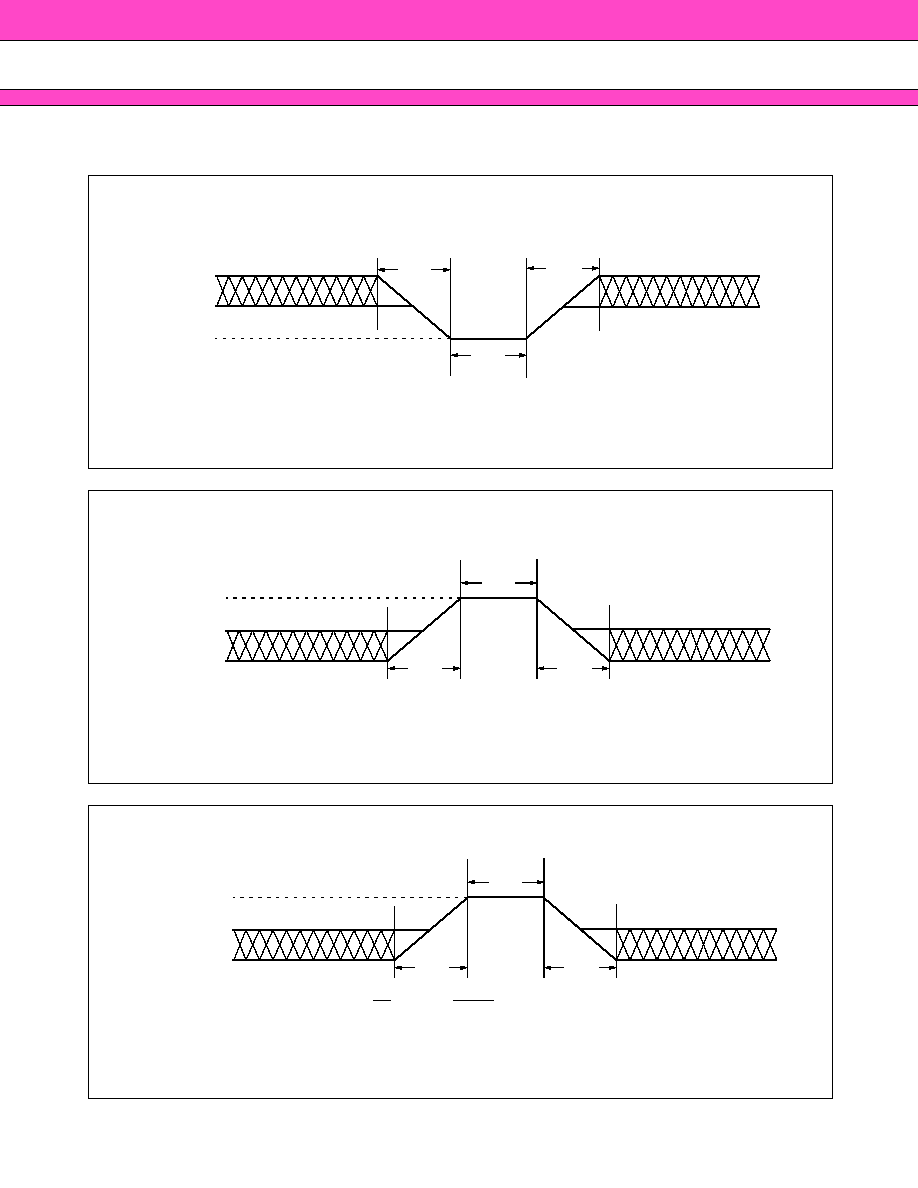
MBM29LV650UE/651UE-
90/12
29
s
s
s
s
MAXIMUM OVERSHOOT/UNDERSHOOT
Figure 1 Maximum Undershoot Waveform
+0.6 V
≠0.5 V
20 ns
≠2.0 V
20 ns
20 ns
Figure 2 Maximum Overshoot Waveform 1
+2.0 V
V
CC
+0.5 V
20 ns
V
CC
+2.0 V
20 ns
20 ns
Figure 3 Maximum Overshoot Waveform 2
V
CC
+0.5 V
+13.0 V
20 ns
+14.0 V
20 ns
20 ns
Note: This waveform is applied for A
9
, OE, ACC
,
and RESET.
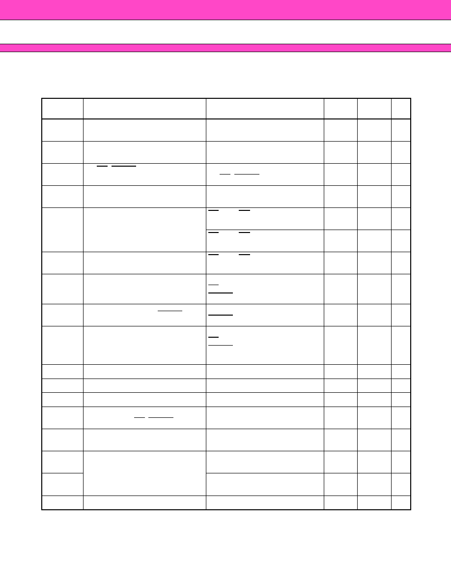
MBM29LV650UE/651UE-
90/12
30
s
s
s
s
ELECTRICAL CHARACTERISTICS
1.
DC Characteristics
Notes: 1. The l
CC
current listed includes both the DC operating current and the frequency dependent component.
2. l
CC
active while Embedded Erase or Embedded Program is in progress.
3. Automatic sleep mode enables the low power mode when address remain stable for 150 ns.
4. Applicable for only V
CC
applying.
Parameter
Symbol
Parameter Description
Test Conditions
Min.
Max.
Unit
I
LI
Input Leakage Current
V
IN
= V
SS
to V
CC
, V
CC
= V
CC
Max.,
V
CC
q = V
CC
q Max.
≠1.0
+1.0
µA
I
LO
Output Leakage Current
V
OUT
= V
SS
to V
CC
, V
CC
= V
CC
Max.,
V
CC
q = V
CC
q Max.
≠1.0
+1.0
µA
I
LIT
A
9
, OE, RESET Inputs Leakage
Current
V
CC
= V
CC
Max.,
A
9
, OE, RESET = 12.5 V
--
35
µA
I
ACC
ACC Accelerated Program Current
V
CC
= V
CC
Max.,
ACC = V
ACC
Max.
--
20
mA
I
CC1
V
CC
Active Current (Note 1)
CE = V
IL
, OE = V
IH
, V
CC
= V
CC
Max.,
V
CC
q = V
CC
q Max., f = 5 MHz
--
16
mA
CE = V
IL
, OE = V
IH
, V
CC
= V
CC
Max.,
V
CC
q = V
CC
q Max., f = 1 MHz
--
7
mA
I
CC2
V
CC
Active Current (Note 2)
CE = V
IL
, OE = V
IH
, V
CC
= V
CC
Max.,
V
CC
q = V
CC
q Max.
--
40
mA
I
CC3
V
CC
Current (Standby)
V
CC
= V
CC
Max., V
CC
q = V
CC
q Max.,
CE = V
CC
±
0.3 V,
RESET = V
CC
±
0.3 V
--
5
µA
I
CC4
V
CC
Current (Standby, RESET)
V
CC
= V
CC
Max., V
CC
q = V
CC
q Max.,
RESET = V
SS
±
0.3 V
--
5
µA
I
CC5
V
CC
Current
(Automatic Sleep Mode) (Note 3)
V
CC
= V
CC
Max., V
CC
q = V
CC
q Max.,
CE = V
SS
±
0.3 V,
RESET = V
CC
±
0.3 V,
V
IN
= V
CC
±
0.3 V or V
SS
±
0.3 V
--
5
µA
V
IL
Input Low Level
--
≠0.5
0.6
V
V
IH
Input High Level
--
2.0
V
CC
+ 0.5
V
V
ACC
Voltage for Program Acceleration
--
11.5
12.5
V
V
ID
Voltage for Autoselect, Sector
Protection (A
9
, OE, RESET) (Note 4)
--
11.5
12.5
V
V
OL
Output Low Voltage Level
I
OL
= 4.0 mA, V
CC
= V
CC
Min.,
V
CC
q = V
CC
q Min.
--
0.45
V
V
OH1
Output High Voltage Level
I
OH
= ≠2.0 mA, V
CC
= V
CC
Min.,
V
CC
q = V
CC
q Min.
2.4
--
V
V
OH2
I
OH
= ≠100 µA, V
CC
Min.,
V
CC
q = V
CC
q Min.
V
CC
q
≠
0.4
--
V
V
LKO
Low V
CC
Lock-Out Voltage
--
2.3
2.5
V

MBM29LV650UE/651UE-
90/12
31
2.
AC Characteristics
∑ Read Only Operations Characteristics
Note: Test Conditions:
Output Load: 1 TTL gate and 30 pF (MBM29LV650UE/651UE-90)
1 TTL gate and 100 pF (MBM29LV650UE/651UE-12)
Input rise and fall times: 5 ns
Input pulse levels: 0.0 V to 3.0 V
Timing measurement reference level
Input: 1.5 V
Output: 1.5 V
Parameter
Symbols
Description
Test Setup
90
(Note)
12
(Note)
Unit
JEDEC
Standard
t
AVAV
t
RC
Read Cycle Time
--
Min.
90
120
ns
t
AVQV
t
ACC
Address to Output Delay
CE = V
IL
OE = V
IL
Max.
90
120
ns
t
ELQV
t
CE
Chip Enable to Output Delay
OE = V
IL
Max.
90
120
ns
t
GLQV
t
OE
Output Enable to Output Delay
--
Max.
35
50
ns
t
EHQZ
t
DF
Chip Enable to Output HIGH-Z
--
Max.
30
30
ns
t
GHQZ
t
DF
Output Enable to Output HIGH-Z
--
Max.
30
30
ns
t
AXQX
t
OH
Output Hold Time From Address,
CE or OE, Whichever Occurs First
--
Min.
0
0
ns
--
t
READY
RESET Pin Low to Read Mode
--
Max.
20
20
µ
s
Figure 4 Test Conditions
C
L
3.3 V
Diodes = IN3064
or Equivalent
2.7 k
Device
Under
Test
IN3064
or Equivalent
6.2 k

MBM29LV650UE/651UE-
90/12
32
∑ Write (Erase/Program) Operations
(Continued)
Parameter Symbols
Description
90
12
Unit
JEDEC
Standard
t
AVAV
t
WC
Write Cycle Time
Min.
90
120
ns
t
AVWL
t
AS
Address Setup Time
Min.
0
0
ns
t
WLAX
t
AH
Address Hold Time
Min.
45
50
ns
t
DVWH
t
DS
Data Setup Time
Min.
35
50
ns
t
WHDX
t
DH
Data Hold Time
Min.
0
0
ns
--
t
OES
Output Enable Setup Time
Min.
0
0
ns
--
t
OEH
Output Enable Hold Time
Read
Min.
0
0
ns
Toggle and Data Polling
Min.
10
10
ns
t
GHWL
t
GHWL
Read Recover Time Before Write
Min.
0
0
ns
t
GHEL
t
GHEL
Read Recover Time Before Write
Min.
0
0
ns
t
ELWL
t
CS
CE Setup Time
Min.
0
0
ns
t
WLEL
t
WS
WE Setup Time
Min.
0
0
ns
t
WHEH
t
CH
CE Hold Time
Min.
0
0
ns
t
EHWH
t
WH
WE Hold Time
Min.
0
0
ns
t
WLWH
t
WP
Write Pulse Width
Min.
35
50
ns
t
ELEH
t
CP
CE Pulse Width
Min.
35
50
ns
t
WHWL
t
WPH
Write Pulse Width High
Min.
30
30
ns
t
EHEL
t
CPH
CE Pulse Width High
Min.
30
30
ns
t
WHWH1
t
WHWH1
Word Programming Operation
Typ.
16
16
µs
t
WHWH2
t
WHWH2
Sector Erase Operation (Note 1)
Typ.
1
1
s
--
t
VCS
V
CC
Setup Time
Min.
50
50
µs
--
t
VIDR
Rise Time to V
ID
(Note 2)
Min.
500
500
ns
--
t
VACCR
Rise Time to V
ACC
(Note 3)
Min.
500
500
ns
--
t
VLHT
Voltage Transition Time (Note 2)
Min.
4
4
µs
--
t
WPP
Write Pulse Width (Note 2)
Min.
100
100
µs
--
t
OESP
OE Setup Time to WE Active (Note 2)
Min.
4
4
µs
--
t
CSP
CE Setup Time to WE Active (Note 2)
Min.
4
4
µs
--
t
RP
RESET Pulse Width
Min.
500
500
ns
--
t
RH
RESET Hold Time Before Read
Min.
200
200
ns

MBM29LV650UE/651UE-
90/12
33
(Continued)
Notes: 1. This does not include the preprogramming time.
2. This timing is for Sector Group Protection operation.
3. This timing is for Accelerated Program operation.
Parameter Symbols
Description
90
12
Unit
JEDEC
Standard
--
t
EOE
Delay Time from Embedded Output Enable
Max.
90
120
ns
--
t
TOW
Erase Time-out Time
Min.
50
50
µs
--
t
SPD
Erase Suspend Transition Time
Max.
20
20
µs

MBM29LV650UE/651UE-
90/12
34
s
s
s
s
ERASE AND PROGRAMMING PERFORMANCE
s
s
s
s
PIN CAPACITANCE
Note: Test conditions T
A
= 25∞C, f = 1.0 MHz
Parameter
Limits
Unit
Comments
Min.
Typ.
Max.
Sector Erase Time
--
1
10
s
Excludes programming time
prior to erasure
Programming Time
--
16
360
µs
Excludes system-level
overhead
Chip Programming Time
--
--
200
s
Excludes system-level
overhead
Erase/Program Cycle
100,000
--
--
cycle
--
Parameter
Symbol
Parameter Description
Test Setup
Typ.
Max.
Unit
C
IN
Input Capacitance
V
IN
= 0
6
7.5
pF
C
OUT
Output Capacitance
V
OUT
= 0
8.5
12
pF
C
IN2
Control Pin Capacitance
V
IN
= 0
8
10
pF
C
IN3
ACC Pin Capacitance
V
IN
= 0
15
20
pF
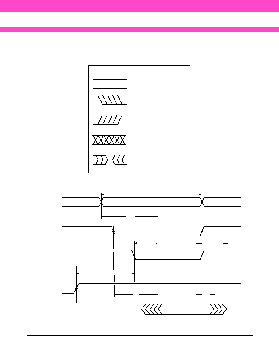
MBM29LV650UE/651UE-
90/12
35
s
s
s
s
TIMING DIAGRAM
∑ Key to Switching Waveforms
Figure 5.1 Read Operation Timing Diagram
WAVEFORM
INPUTS
OUTPUTS
Must Be
Steady
May
Change
from H to L
May
Change
from L to H
"H" or "L"
Any Change
Permitted
Does Not
Apply
Will Be
Steady
Will Be
Changing
from H to L
Will Be
Changing
from L to H
Changing
State
Unknown
Center Line is
High-
Impedance
"Off" State
WE
OE
CE
t
ACC
t
DF
t
CE
t
OH
t
OE
Outputs
t
RC
Addresses
Addresses Stable
High-Z
Output Valid
High-Z
t
OEH
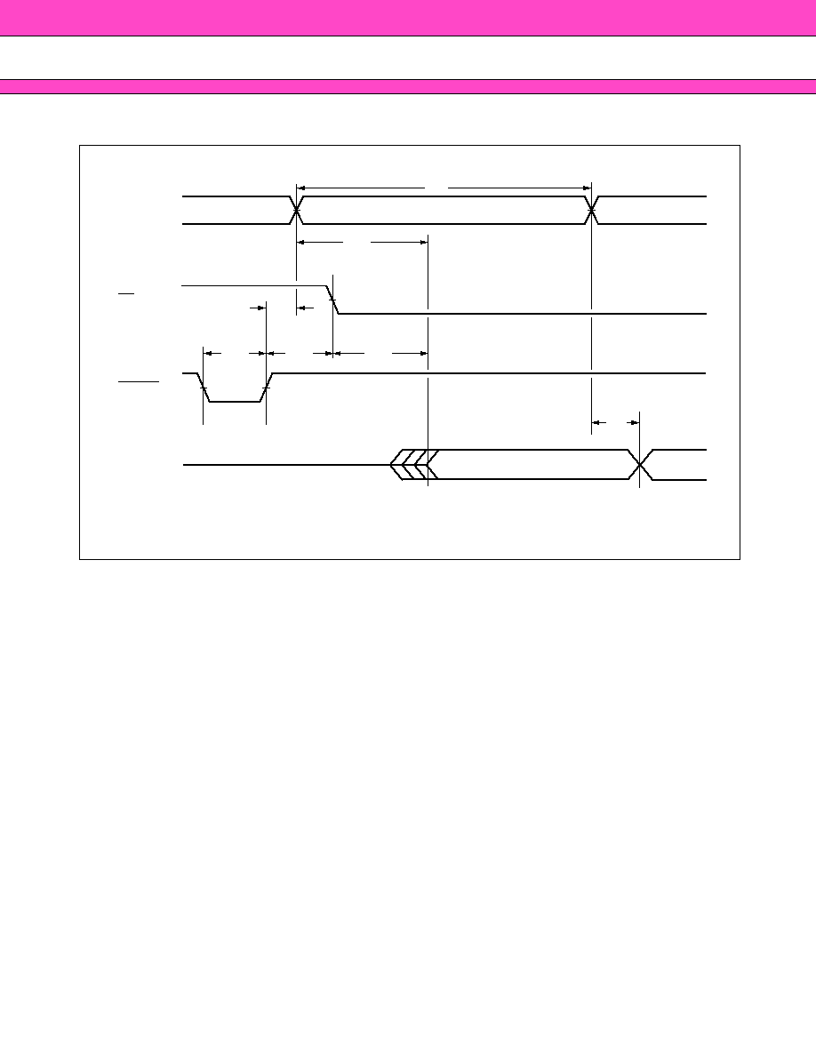
MBM29LV650UE/651UE-
90/12
36
Figure 5.2 Hardware Reset/Read Operation Timing Diagram
RESET
t
ACC
t
OH
Outputs
t
RC
Addresses
Addresses Stable
High-Z
Output Valid
t
RH
CE
t
RP
t
RH
t
CE
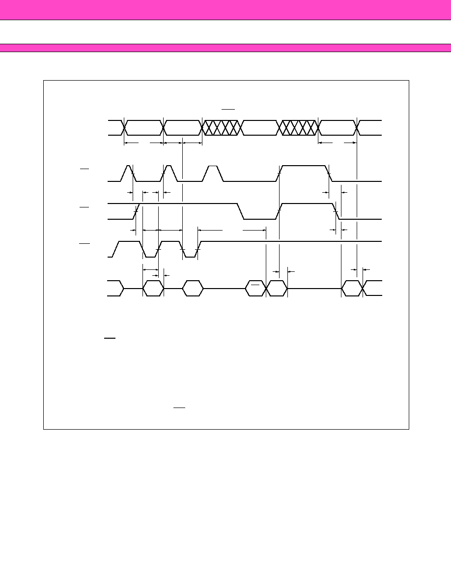
MBM29LV650UE/651UE-
90/12
37
Notes: 1. PA is address of the memory location to be programmed.
2. PD is data to be programmed at byte address.
3. DQ
7
is the output of the complement of the data written to the device.
4. D
OUT
is the output of the data written to the device.
5. Figure indicates last two bus cycles out of four bus cycle sequence.
Figure 6 Alternate WE Controlled Program Operation Timing Diagram
t
CH
t
WP
t
WHWH1
t
WC
t
AH
CE
OE
t
RC
Addresses
Data
t
AS
t
OE
t
WPH
t
GHWL
t
DH
DQ
7
PD
A0h
D
OUT
WE
XXXh
PA
PA
t
OH
Data Polling
3rd Bus Cycle
t
CS
t
CE
t
DS
D
OUT
t
DF
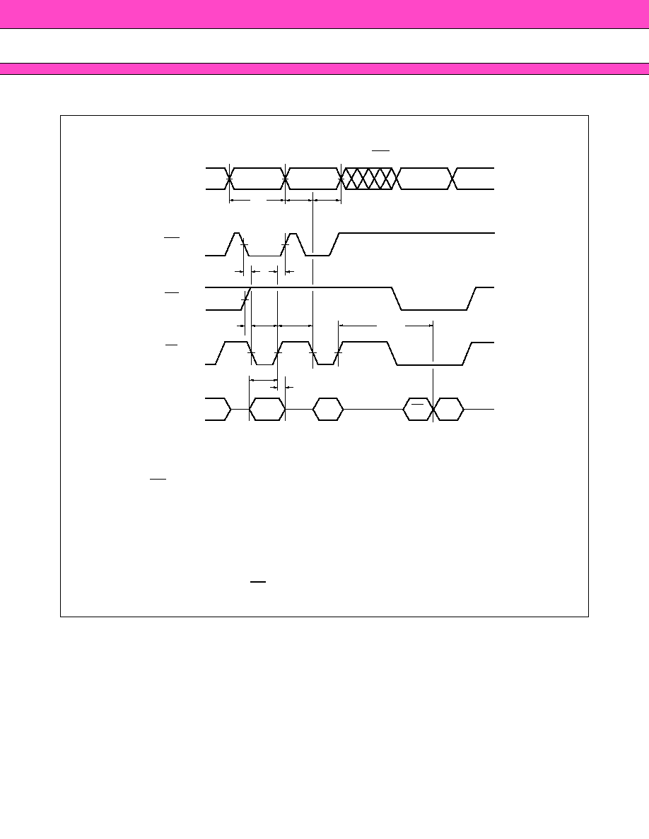
MBM29LV650UE/651UE-
90/12
38
Figure 7 Alternate CE Controlled Program Operation Timing Diagram
Notes: 1. PA is address of the memory location to be programmed.
2. PD is data to be programmed at byte address.
3. DQ
7
is the output of the complement of the data written to the device.
4. D
OUT
is the output of the data written to the device.
5. Figure indicates last two bus cycles out of four bus cycle sequence.
t
CP
t
DS
t
WHWH1
t
WC
t
AH
WE
OE
Addresses
Data
t
AS
t
CPH
t
DH
DQ
7
A0h
D
OUT
CE
XXXh
PA
PA
Data Polling
3rd Bus Cycle
t
WS
t
WH
t
GHEL
PD

MBM29LV650UE/651UE-
90/12
39
Figure 8 Chip/Sector Erase Operation Timing Diagram
* : SA is the sector address for Sector Erase. Addresses = XXXh for Chip Erase.
V
CC
CE
OE
Addresses
Data
t
WP
WE
XXXh
XXXh
XXXh
XXXh
XXXh
SA *
t
DS
t
CH
t
AS
t
AH
t
CS
t
WPH
t
DH
t
GHWL
t
VCS
t
WC
55h
55h
80h
AAh
AAh
10h/
30h
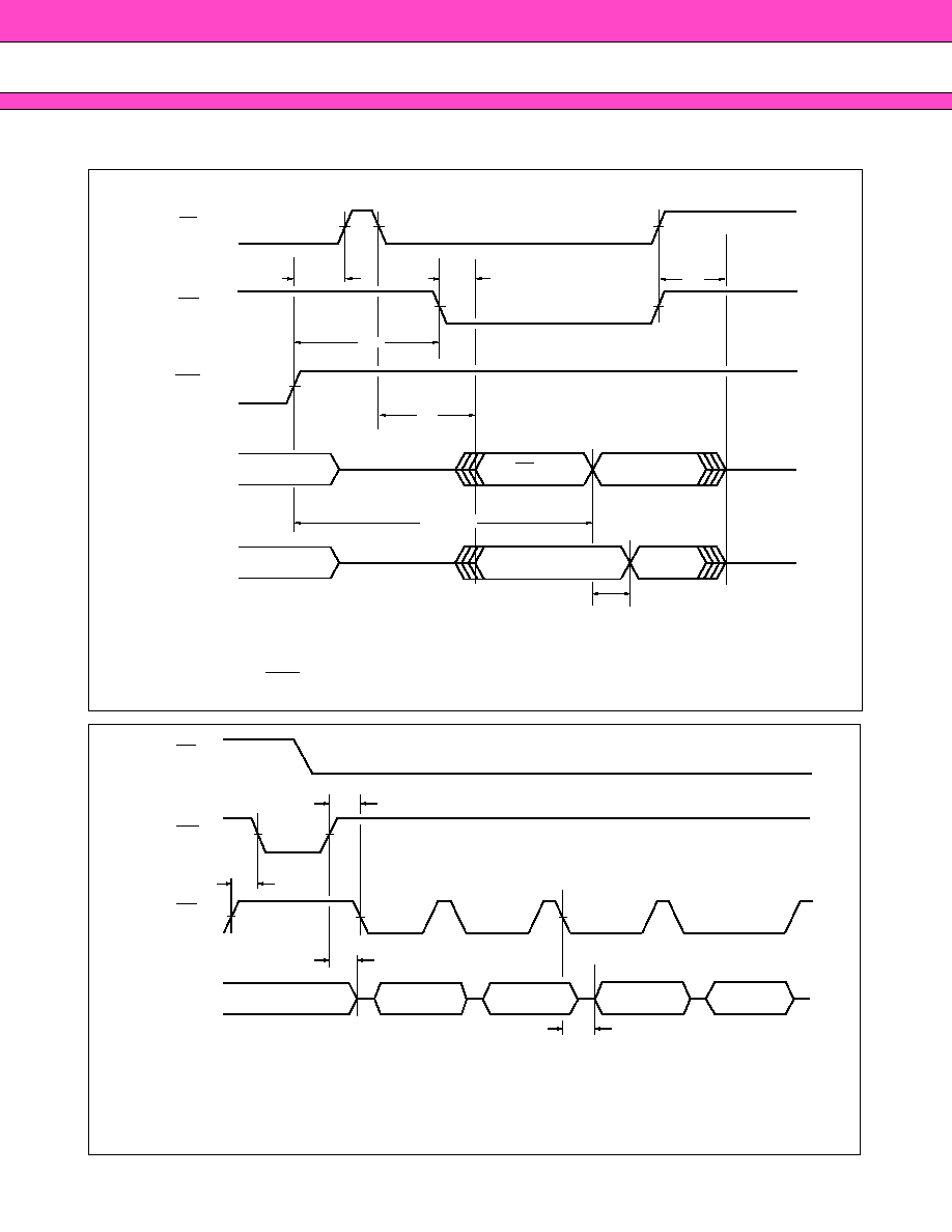
MBM29LV650UE/651UE-
90/12
40
Figure 9 Data Polling during Embedded Algorithm Operation Timing Diagram
* : DQ
7
= Valid Data (The device has completed the Embedded operation.)
t
OEH
t
OE
t
WHWH1 or 2
CE
OE
t
EOE
WE
t
DF
t
CH
t
CE
High-Z
High-Z
DQ
7
=
Valid Data
DQ
0
to DQ
6
Valid Data
DQ
7
*
DQ
7
DQ
0
to DQ
6
Data
Data
DQ
0
to DQ
6
= Output Flag
*
Figure 10 Toggle Bit I during Embedded Algorithm Operation Timing Diagram
* : DQ
6
= Stops toggling. (The device has completed the Embedded operation.)
CE
WE
OE
Data (DQ
0
to DQ
7
)
DQ
6
= Toggle
DQ
6
=
Stop Toggling
DQ
0
to DQ
7
Data Valid
t
OE
DQ
6
= Toggle
t
OEH
t
OES
t
DH
DQ
6

MBM29LV650UE/651UE-
90/12
41
Figure 11 DQ
2
vs. DQ
6
DQ
2
DQ
6
WE
Erase
Erase
Suspend
Enter
Embedded
Erasing
Erase Suspend
Read
Enter Erase
Suspend Program
Erase
Suspend
Program
Erase Suspend
Read
Erase
Resume
Erase
Erase
Complete
Toggle
DQ
2
and DQ
6
with OE or CE
Note: DQ
2
is read from the erase-suspended sector.

MBM29LV650UE/651UE-
90/12
42
Figure 12 Sector Group Protection Timing Diagram
SGAX = Sector Group Address for initial sector
SGAY = Sector Group Address for next sector
t
VLHT
SGAX
A
21
, A
20
, A
19
A
18
, A
17
SGAY
A
0
A
6
A
9
3 V
t
VLHT
OE
3 V
t
VLHT
t
VLHT
t
OESP
t
WPP
t
CSP
WE
CE
t
OE
01h
Data
V
CC
A
1
t
VCS
V
ID
V
ID

MBM29LV650UE/651UE-
90/12
43
3 V
RESET
V
CC
CE
WE
t
VLHT
Program or Erase Command Sequence
3 V
t
VLHT
t
VCS
t
VIDR
V
ID
t
VLHT
Unprotection period
Figure 13 Temporary Sector Group Unprotection Timing Diagram
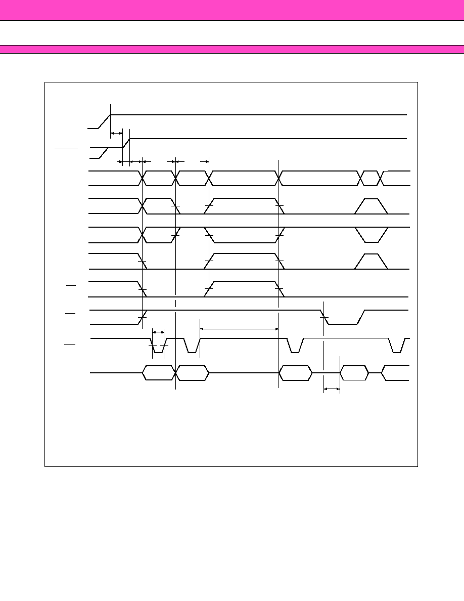
MBM29LV650UE/651UE-
90/12
44
Figure 14 Extended Sector Group Protection Timing Diagram
SGAX: Sector Group Address to be protected
SGAY : Next Sector Group Address to be protected
TIME-OUT : Time-Out window = 250
µ
s (min)
SGAY
RESET
A
6
OE
WE
CE
Data
A
1
V
CC
A
0
Add
SGAX
SGAX
60h
01h
40h
60h
60h
TIME-OUT
t
VCS
t
VLHT
t
VIDR
t
OE
t
WP
t
WC
t
WC
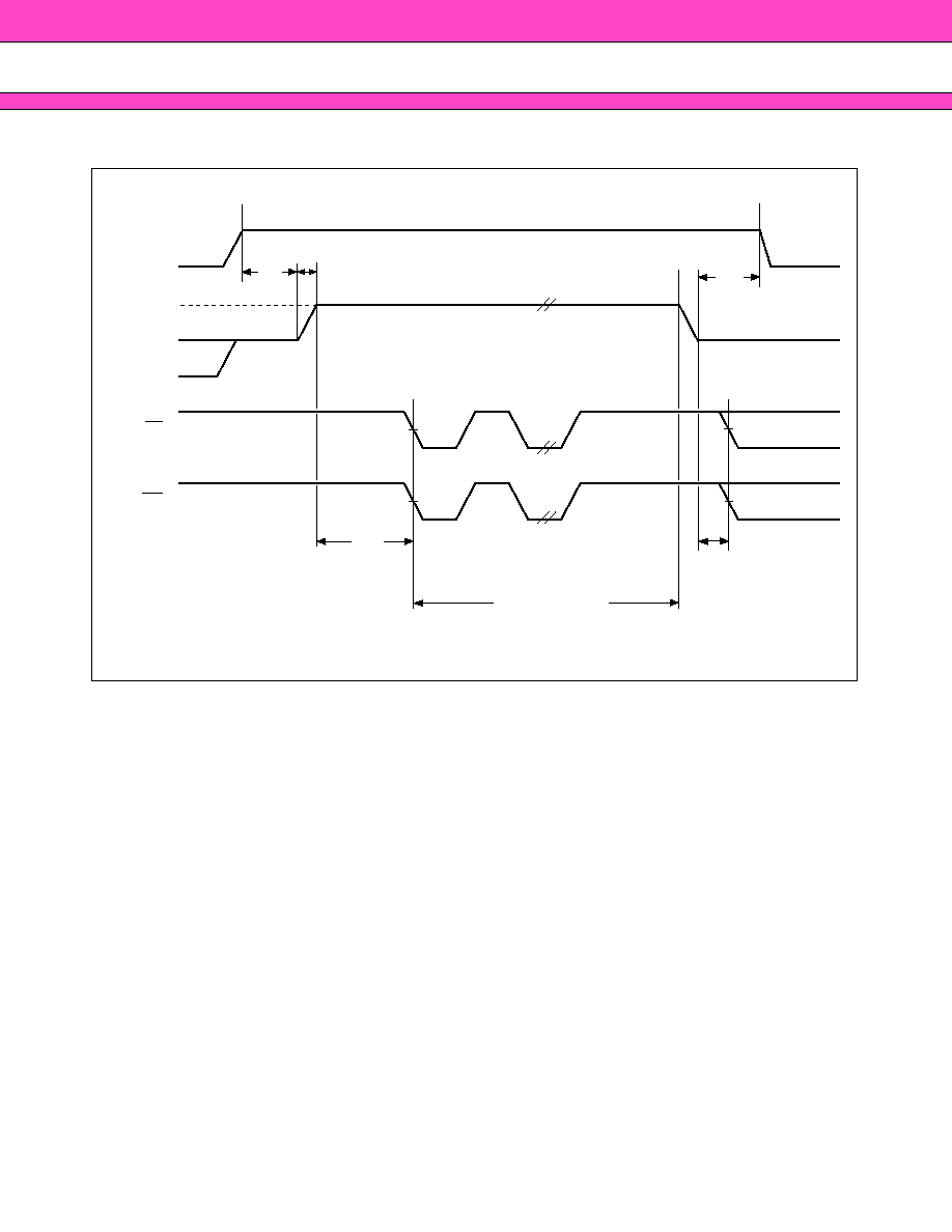
MBM29LV650UE/651UE-
90/12
45
Figure 15 Accelerated Program Timing Diagram
3 V
ACC
V
CC
CE
WE
t
VLHT
Program or Erase Command Sequence
3 V
t
VLHT
t
VCS
t
VACCR
V
ACC
t
VLHT
Acceleration period
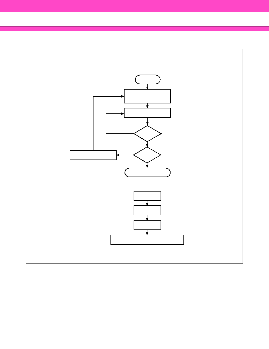
MBM29LV650UE/651UE-
90/12
46
s
s
s
s
FLOW CHART
Write Program Command
Sequence
(See below)
Data Polling
Program Command Sequence (Address/Command):
XXXh/AAh
XXXh/55h
XXXh/A0h
Program Address/Program Data
Start
No
Yes
Increment Address
Last Address
?
Programming Completed
Embeded
Program
Algorithm
in progress
Verify Data
?
No
Yes
Figure 16 Embedded Program
TM
Algorithm
EMBEDDED ALGORITHMS

MBM29LV650UE/651UE-
90/12
47
Write Erase Command
Sequence
(See below)
Data Polling
Erasure Completed
Start
XXXh/AAh
XXXh/55h
XXXh/AAh
XXXh/80h
XXXh/10h
XXXh/55h
XXXh/AAh
XXXh/55h
XXXh/AAh
XXXh/80h
XXXh/55h
Additional sector
erase commands
are optional.
Chip Erase Command Sequence
(Address/Command):
Individual Sector/Multiple Sector
Erase Command Sequence
(Address/Command):
Sector Address/30h
Sector Address/30h
Sector Address/30h
Data=FFh
?
Embeded
Program
Algorithm
in progress
No
Yes
Figure 17 Embedded Erase
TM
Algorithm
EMBEDDED ALGORITHMS

MBM29LV650UE/651UE-
90/12
48
DQ
7
= Data?
*
No
No
DQ
7
= Data?
DQ
5
= 1?
Yes
Yes
No
Read Byte
(DQ
7
to DQ
0
)
Addr. = VA
Read Byte
(DQ
7
to DQ
0
)
Addr. = VA
Yes
Start
Fail
Pass
Figure 18 Data Polling Algorithm
*
DQ
7
is rechecked even if DQ
5
= "1" because DQ
7
may change simultaneously with DQ
5
.
VA = Byte address for programming
= Any of the sector addresses within
the sector being erased during
sector erase or multiple sector
erases operation
= Any of the sector addresses within
the sector not being protected
during chip erase

MBM29LV650UE/651UE-
90/12
49
Toggle Bit
= Toggle
?
Yes
No
Toggle Bit
= Toggle
?
DQ
5
= 1?
Yes
No
No
Yes
Start
*1,*2
*1
Read DQ
7
to DQ
0
Twice
Read DQ
7
to DQ
0
Program/Erase
Operation Not
Complete.Write
Reset Command
Program/Erase
Operation Complete
Read DQ
7
to DQ
0
Figure 19 Toggle Bit Algorithm
*1:Reset toggle bit twice to determine whether or not it is toggle.
*2:Recheck toggle bit because it may stop toggle as DQ5 changes to "1" .
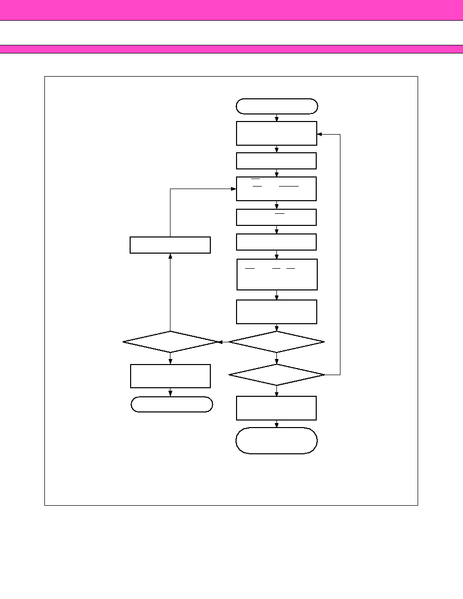
MBM29LV650UE/651UE-
90/12
50
Setup Sector Group Addr.
(A
21
, A
20
, A
19
, A
18
, A
17
)
Activate WE Pulse
WE = V
IH
, CE = OE = V
IL
(A
9
should remain V
ID
)
Yes
Yes
No
No
OE = V
ID
, A
9
= V
ID
,
A
6
= CE = V
IL
, RESET = V
IH
A
0
= V
IL
, A
1
= V
IH
PLSCNT = 1
Time out 100
µ
s
Read from Sector Group
(Addr. = SGA, A
0
= V
IL
,
A
1
= V
IH
, A
6
= V
IL
)
Remove V
ID
from A
9
Write Reset Command
Increment PLSCNT
No
Yes
Protect Another Sector
Group ?
Data = 01h?
PLSCNT = 25?
Remove V
ID
from A
9
Write Reset Command
Start
Sector Group Protection
Completed
Device Failed
Figure 20 Sector Group Protection Algorithm

MBM29LV650UE/651UE-
90/12
51
RESET = V
ID
* 1
Perform Erase or
Program Operations
RESET = V
IH
Start
Temporary Sector Group
Unprotection Completed
* 2
Figure 21 Temporary Sector Group Unprotection Algorithm
*1: All protected sector groups are unprotected.
*2: All previously protected sector groups are protected once again.

MBM29LV650UE/651UE-
90/12
52
To Sector Group Protection
Yes
No
No
PLSCNT = 1
Protection Other Sector
Start
Sector Group Protection
Extended Sector Group
Completed
Remove
V
ID
from RESET
Write Reset Command
RESET = V
ID
Wait to 4
µ
s
Protection Entry?
To Setup Sector Group
Protection Write XXXh/60h
Write SGA/60h
(A
0
= V
IL
, A
1
= V
IH
, A
6
= V
IL
)
Time Out 250
µ
s
To Verify Sector Group
Protection Write SGA/40h
(A
0
= V
IL
, A
1
= V
IH
, A
6
= V
IL
)
Data = 01h?
Group?
Device is Operating in
Temporary Sector Group
Read from Sector Group
(A
0
= V
IL
, A
1
= V
IH
, A
6
= V
IL
)
Increment PLSCNT
No
Yes
Yes
Unprotection Mode
Address
Setup Next Sector Group
Address
No
Yes
PLSCNT = 25?
Device Failed
Remove V
ID
from RESET
Write Reset Command
Figure 22 Extended Sector Group Protection Algorithm
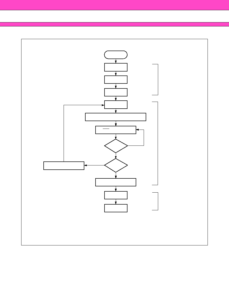
MBM29LV650UE/651UE-
90/12
53
Figure 23 Embedded Program
TM
Algorithm for Fast Mode
FAST MODE ALGORITHM
Start
XXXh/AAh
XXXh/55h
XXXh/A0h
XXXh/20h
Verify Data?
No
Program Address/Program Data
Data Polling Device
Last Address
?
Programming Completed
XXXh/90h
XXXh/F0h
Increment Address
No
Yes
Yes
Set Fast Mode
In Fast Program
Reset Fast Mode

MBM29LV650UE/651UE-
90/12
54
s
s
s
s
ORDERING INFORMATION
Standard Products
Fujitsu standard products are available in several packages. The order number is formed by a combination of:
MBM29LV650U(651U)
E
90
TN
DEVICE NUMBER/DESCRIPTION
MBM29LV650U(651U)
64 Mega-bit (4M
◊
16-Bit) CMOS Flash Memory
3.0 V-only Read, Program, and Erase
PACKAGE TYPE
TN= 48-Pin Thin Small Outline Package
(TSOP) Standard Pinout
TR = 48-Pin Thin Small Outline Package
(TSOP) Reverse Pinout
SPEED OPTION
See Product Selector Guide
DEVICE REVISION
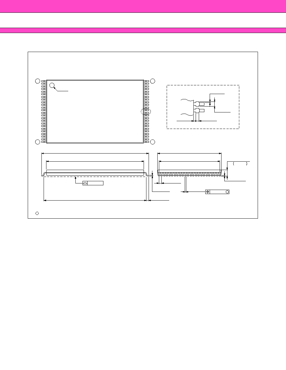
MBM29LV650UE/651UE-
90/12
55
s
s
s
s
PACKAGE DIMENSIONS
(Continued)
C
2000 FUJITSU LIMITED F48029S-3c-4
Details of "A" part
0.15(.006)
MAX
0.35(.014)
MAX
0.15(.006)
0.25(.010)
INDEX
"A"
18.40±0.20
(.724±.008)
20.00±0.20
(.787±.008)
19.00±0.20
(.748±.008)
0.50±0.10
(.020±.004)
0.15±0.05
(.006±.002)
11.50REF
(.453)
0.50(.0197)
TYP
0.20±0.10
(.008±.004)
0.10±0.05
.043
≠.002
+.004
≠0.05
+0.10
1.10
M
0.10(.004)
(.004±.002)
1
24
25
48
LEAD No.
*
*
12.00±0.20
(.472±.008)
(Mounting height)
0.10(.004)
(STAND OFF)
Dimensions in mm (inches)
48-pin plastic TSOP (I)
(FPT-48P-M19)
*: Resin protrusion. (Each side: 0.15(.006) Max)
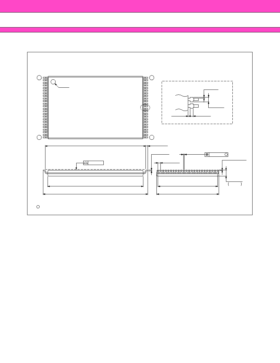
MBM29LV650UE/651UE-
90/12
56
(Continued)
C
2000 FUJITSU LIMITED F48030S-3c-4
Details of "A" part
0.15(.006)
MAX
0.35(.014)
MAX
0.15(.006)
0.25(.010)
INDEX
"A"
18.40±0.20
(.724±.008)
20.00±0.20
(.787±.008)
19.00±0.20
(.748±.008)
0.50±0.10
(.020±.004)
0.15±0.05
(.006±.002)
11.50(.453)REF
0.50(.020)
TYP
0.20±0.10
(.008±.004)
.043
≠.002
+.004
≠0.05
+0.10
1.10
M
0.10(.004)
1
24
25
48
LEAD No.
*
*
12.00±0.20(.472±.008)
(Mounting height)
0.10(.004)
0.10±0.05
(.004±.002)
(STAND OFF)
Dimensions in mm (inches)
48-pin plastic TSOP (I)
(FPT-48P-M20)
*: Resin protrusion. (Each side: 0.15(.006) Max)

MBM29LV650UE/651UE-
90/12
FUJITSU LIMITED
For further information please contact:
Japan
FUJITSU LIMITED
Corporate Global Business Support Division
Electronic Devices
Shinjuku Dai-Ichi Seimei Bldg. 7-1,
Nishishinjuku 2-chome, Shinjuku-ku,
Tokyo 163-0721, Japan
Tel: +81-3-5322-3347
Fax: +81-3-5322-3386
http://edevice.fujitsu.com/
North and South America
FUJITSU MICROELECTRONICS, INC.
3545 North First Street,
San Jose, CA 95134-1804, U.S.A.
Tel: +1-408-922-9000
Fax: +1-408-922-9179
Customer Response Center
Mon. - Fri.: 7 am - 5 pm (PST)
Tel: +1-800-866-8608
Fax: +1-408-922-9179
http://www.fujitsumicro.com/
Europe
FUJITSU MICROELECTRONICS EUROPE GmbH
Am Siebenstein 6-10,
D-63303 Dreieich-Buchschlag,
Germany
Tel: +49-6103-690-0
Fax: +49-6103-690-122
http://www.fujitsu-fme.com/
Asia Pacific
FUJITSU MICROELECTRONICS ASIA PTE. LTD.
#05-08, 151 Lorong Chuan,
New Tech Park,
Singapore 556741
Tel: +65-281-0770
Fax: +65-281-0220
http://www.fmap.com.sg/
Korea
FUJITSU MICROELECTRONICS KOREA LTD.
1702 KOSMO TOWER, 1002 Daechi-Dong,
Kangnam-Gu,Seoul 135-280
Korea
Tel: +82-2-3484-7100
Fax: +82-2-3484-7111
F0012
©
FUJITSU LIMITED Printed in Japan
All Rights Reserved.
The contents of this document are subject to change without notice.
Customers are advised to consult with FUJITSU sales
representatives before ordering.
The information and circuit diagrams in this document are
presented as examples of semiconductor device applications, and
are not intended to be incorporated in devices for actual use. Also,
FUJITSU is unable to assume responsibility for infringement of
any patent rights or other rights of third parties arising from the use
of this information or circuit diagrams.
The contents of this document may not be reproduced or copied
without the permission of FUJITSU LIMITED.
FUJITSU semiconductor devices are intended for use in standard
applications (computers, office automation and other office
equipments, industrial, communications, and measurement
equipments, personal or household devices, etc.).
CAUTION:
Customers considering the use of our products in special
applications where failure or abnormal operation may directly
affect human lives or cause physical injury or property damage, or
where extremely high levels of reliability are demanded (such as
aerospace systems, atomic energy controls, sea floor repeaters,
vehicle operating controls, medical devices for life support, etc.)
are requested to consult with FUJITSU sales representatives before
such use. The company will not be responsible for damages arising
from such use without prior approval.
Any semiconductor devices have inherently a certain rate of failure.
You must protect against injury, damage or loss from such failures
by incorporating safety design measures into your facility and
equipment such as redundancy, fire protection, and prevention of
over-current levels and other abnormal operating conditions.
If any products described in this document represent goods or
technologies subject to certain restrictions on export under the
Foreign Exchange and Foreign Trade Control Law of Japan, the
prior authorization by Japanese government should be required for
export of those products from Japan.