 | –≠–ª–µ–∫—Ç—Ä–æ–Ω–Ω—ã–π –∫–æ–º–ø–æ–Ω–µ–Ω—Ç: 29LV800BE | –°–∫–∞—á–∞—Ç—å:  PDF PDF  ZIP ZIP |

September 2003
This document specifies SPANSION
memory products that are now offered by both Advanced Micro Devices and
Fujitsu. Although the document is marked with the name of the company that originally developed the specification,
these products will be offered to customers of both AMD and Fujitsu.
Continuity of Specifications
There is no change to this datasheet as a result of offering the device as a SPANSION
product. Future routine
revisions will occur when appropriate, and changes will be noted in a revision summary.
Continuity of Ordering Part Numbers
AMD and Fujitsu continue to support existing part numbers beginning with "Am" and "MBM". To order these
products, please use only the Ordering Part Numbers listed in this document.
For More Information
Please contact your local AMD or Fujitsu sales office for additional information about SPANSION
memory
solutions.
TM
TM
TM
SPANSION Flash Memory
Data Sheet
TM
DS05-20888-6E
FUJITSU SEMICONDUCTOR
DATA SHEET
FLASH MEMORY
CMOS
8 M (1 M
◊
◊
◊
◊
8/512 K
◊
◊
◊
◊
16) BIT
MBM29LV800TE
60/70/90
/MBM29LV800BE
60/70/90
s
DESCRIPTION
The MBM29LV800TE/BE are a 8 M-bit, 3.0 V-only Flash memory organized as 1 M bytes of 8 bits each or
512 Kwords of 16 bits each. The MBM29LV800TE/BE are offered in a 48-pin TSOP (1) , 48-pin CSOP and 48-
ball FBGA package. These devices are designed to be programmed in a system with the standard system 3.0 V
V
CC
supply. 12.0 V V
PP
and 5.0 V V
CC
are not required for write or erase operations. The devices can also be
reprogrammed in standard EPROM programmers.
(Continued)
s
PRODUCT LINE UP
s
PACKAGES
Part No.
MBM29LV800TE/BE
Ordering Part No.
V
CC
=
3.3 V
60
V
CC
=
3.0 V
70
90
Max Address Access Time (ns)
60
70
90
Max CE Access Time (ns)
60
70
90
Max OE Access Time (ns)
30
30
35
48-pin Plastic TSOP (1)
48-pin Plastic CSOP
48-ball Plastic FBGA
(FPT-48P-M19)
(LCC-48P-M03)
(BGA-48P-M20)
+
0.3 V
-
0.3 V
+
0.6 V
-
0.3 V

MBM29LV800TE/BE
60/70/90
2
(Continued)
The standard MBM29LV800TE/BE offer access times 60 ns, 70 ns and 90 ns, allowing operation of high-speed
microprocessors without wait state. To eliminate bus contention, the devices have separate chip enable (CE) ,
write enable (WE) , and output enable (OE) controls.
The MBM29LV800TE/BE are pin and command set compatible with JEDEC standard E
2
PROMs. Commands
are written to the command register using standard microprocessor write timings. Register contents serve as
input to an internal state-machine which controls the erase and programming circuitry. Write cycles also internally
latch addresses and data needed for the programming and erase operations. Reading data out of the devices
is similar to reading from 5.0 V and 12.0 V Flash or EPROM devices.
The MBM29LV800TE/BE are programmed by executing the program command sequence. This will invoke the
Embedded Program Algorithm which is an internal algorithm that automatically times the program pulse widths
and verifies proper cell margin. Typically, each sector can be programmed and verified in about 0.5 seconds.
Erase is accomplished by executing the erase command sequence. This will invoke the Embedded Erase
Algorithm which is an internal algorithm that automatically preprograms the array if it is not already programmed
before executing the erase operation. During erase, the devices automatically time the erase pulse widths and
verify proper cell margin.
A sector is typically erased and verified in 1.0 second. (If already completely preprogrammed.)
The devices also feature a sector erase architecture. The sector mode allows each sector to be erased and
reprogrammed without affecting other sectors. The MBM29LV800TE/BE are erased when shipped from the
factory.
The devices feature single 3.0 V power supply operation for both read and write functions. Internally generated
and regulated voltages are provided for the program and erase operations. A low V
CC
detector automatically
inhibits write operations on the loss of power. The end of program or erase is detected by Data Polling of DQ
7
,
by the Toggle Bit feature on DQ
6
, or the RY/BY output pin. Once the end of a program or erase cycle has been
completed, the devices internally resets to the read mode.
The MBM29LV800TE/BE also have hardware RESET pins. When this pin is driven low, execution of any
Embedded Program Algorithm or Embedded Erase Algorithm is terminated. The internal state machine is then
reset to the read mode. The RESET pin may be tied to the system reset circuitry. Therefore, if a system reset
occurs during the Embedded Program Algorithm or Embedded Erase Algorithm, the device is automatically
reset to the read mode and will have erroneous data stored in the address locations being programmed or
erased. These locations need re-writing after the Reset. Resetting the device enables the system's
microprocessor to read the boot-up firmware from the Flash memory.
Fujitsu's Flash technology combines years of Flash memory manufacturing experience to produce the highest
levels of quality, reliability, and cost effectiveness. The MBM29LV800TE/BE memory electrically erase all bits
within a sector simultaneously via Fowler-Nordhiem tunneling. The bytes/words are programmed one byte/word
at a time using the EPROM programming mechanism of hot electron injection.

MBM29LV800TE/BE
60/70/90
3
s
FEATURES
∑ 0.23
µ
µ
µ
µ
m Process Technology
∑ Single 3.0 V Read, Program, and Erase
Minimized system level power requirements
∑ Compatible with JEDEC-standard Commands
Use the same software commands as E
2
PROMs
∑ Compatible with JEDEC-standard World-wide Pinouts
48-pin TSOP (1) (Package suffix : TN Normal Bend Type)
48-pin CSOP (Package suffix : PCV)
48-ball FBGA (Package suffix : PBT)
∑ Minimum 100,000 Program/Erase Cycles
∑ High Performance
70 ns maximum access time
∑ Sector Erase Architecture
One 8 Kwords, two 4 Kwords, one 16 Kwords, and fifteen 32 Kwords sectors in word mode
One 16 Kbytes, two 8 Kbytes, one 32 Kbytes, and fifteen 64 Kbytes sectors in byte mode
Any combination of sectors can be concurrently erased, and also supports full chip erase.
∑ Boot Code Sector Architecture
T
=
Top sector
B
=
Bottom sector
∑ Embedded Erase
TM
* Algorithm
Automatically pre-programs and erases the chip or any sector.
∑ Embedded Program
TM
* Algorithm
Automatically writes and verifies data at specified address.
∑ Data Polling and Toggle Bit Feature for Detection of Program or Erase Cycle Completion
∑ Ready/Busy Output (RY/BY)
Hardware method for detection of program or erase cycle completion
∑ Automatic Sleep Mode
When addresses remain stable, MBM29LV800TE/BE automatically switch themselves to low power mode.
∑ Low V
CC
Write Inhibit
2.5 V
∑ Erase Suspend/Resume
Suspends the erase operation to allow a read data and/or program in another sector within the same device.
∑ Sector Protection
Hardware method disables any combination of sectors from program or erase operations.
∑ Sector Protection Set Function by Extended Sector Protection Command
∑ Fast Programming Function by Extended Command
∑ Temporary Sector Unprotection
Temporary sector unprotection via the RESET pin
* : Embedde Erase
TM
and Embedded Program
TM
are trademarks of Advanced Micro Devices, Inc.
MBM29LV800TE/BE
60/70/90
4
s
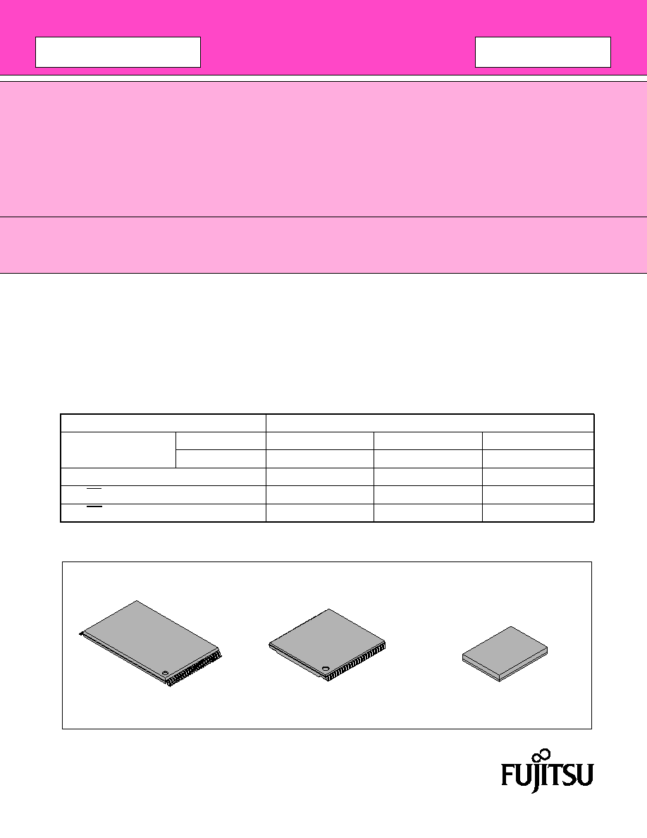
PIN ASSIGNMENTS
(Continued)
48
N.C.
1
2
3
4
5
6
7
8
9
10
11
12
13
14
15
16
17
18
19
20
21
22
23
24
47
35
46
45
44
43
42
41
40
39
38
37
36
34
33
32
31
30
29
28
27
26
25
A
3
A
2
A
4
A
1
A
6
A
7
A
18
A
17
RY/BY
N.C.
WE
RESET
N.C.
N.C.
A
8
A
9
A
10
A
11
A
13
A
12
A
14
A
15
A
0
DQ
1
DQ
8
DQ
0
OE
V
SS
CE
DQ
2
DQ
9
DQ
10
DQ
3
DQ
11
V
CC
DQ
4
DQ
12
DQ
5
DQ
14
DQ
6
DQ
13
DQ
7
BYTE
V
SS
DQ
15
/A
-1
A
16
A
5
MBM29LV800TE/MBM29LV800BE
Normal Bend
(Marking Side)
TSOP (1)
(FPT-48P-M19)
MBM29LV800TE/BE
60/70/90
5
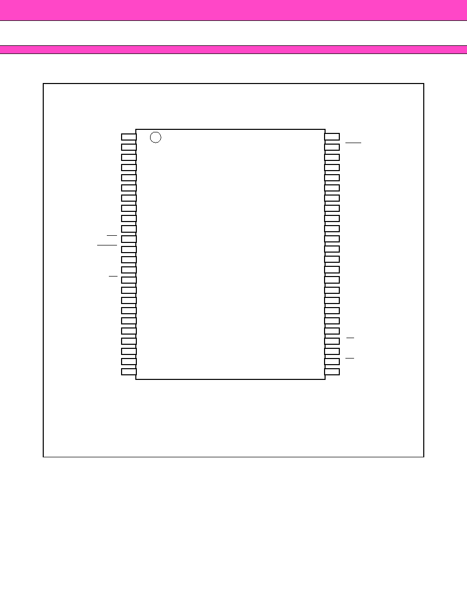
(Continued)
(Marking side)
1
2
3
4
5
6
7
8
9
10
11
12
13
14
15
16
17
18
19
20
21
22
23
24
A
0
CE
V
SS
OE
DQ
0
DQ
8
DQ
1
DQ
9
DQ
2
DQ
10
DQ
3
DQ
11
V
CC
DQ
4
DQ
12
DQ
5
DQ
13
DQ
6
DQ
14
DQ
7
DQ
15
/A
-1
V
SS
BYTE
A
16
48
47
46
45
44
43
42
41
40
39
38
37
36
35
34
33
32
31
30
29
28
27
26
25
A
1
A
2
A
3
A
4
A
5
A
6
A
7
A
17
A
18
RY/BY
N.C.
N.C.
RESET
WE
N.C.
N.C.
A
8
A
9
A
10
A
11
A
12
A
13
A
14
A
15
CSOP
(TOP VIEW)
(LCC-48P-M03)

MBM29LV800TE/BE
60/70/90
6
(Continued)
H1
A1
A2
A3
A4
A5
A6
F1
F2
F3
F4
B1
B2
B3
B4
B5
B6
F5
F6
G4
G5
C1
C2
C3
C4
H2
D5
E6
E5
E4
E3
E2
E1
H3
H4
G6
D6
D4
D3
D2
D1
G1
G2
G3
C6
C5
H5
H6
FBGA
(TOP VIEW)
Marking side
(BGA-48P-M20)
A1
A
3
A2
A
7
A3
RY/BY
A4
WE
A5
A
9
A6
A
13
B1
A
4
B2
A
17
B3
N.C.
B4
RESET
B5
A
8
B6
A
12
C1
A
2
C2
A
6
C3
A
18
C4
N.C.
C5
A
10
C6
A
14
D1
A
1
D2
A
5
D3
N.C.
D4
N.C.
D5
A
11
D6
A
15
E1
A
0
E2
DQ
0
E3
DQ
2
E4
DQ
5
E5
DQ
7
E6
A
16
F1
CE
F2
DQ
8
F3
DQ
10
F4
DQ
12
F5
DQ
14
F6
BYTE
G1
OE
G2
DQ
9
G3
DQ
11
G4
V
CC
G5
DQ
13
G6
DQ
15
/A
-1
H1
V
SS
H2
DQ
1
H3
DQ
3
H4
DQ
4
H5
DQ
6
H6
V
SS

MBM29LV800TE/BE
60/70/90
7
s
PIN DESCRIPTION
Pin name
Function
A
18
to A
0
, A
-1
Address Inputs
DQ
15
to DQ
0
Data Inputs/Outputs
CE
Chip Enable
OE
Output Enable
WE
Write Enable
RY/BY
Ready/Busy Output
RESET
Hardware Reset Pin/Temporary Sector Unprotection
BYTE
Selects 8-bit or 16-bit mode
N.C.
No Internal Connection
V
SS
Device Ground
V
CC
Device Power Supply

MBM29LV800TE/BE
60/70/90
8
s
BLOCK DIAGRAM
s
LOGIC SYMBOL
A
-1
V
SS
V
CC
WE
CE
A
18
to A
0
OE
DQ
15
to DQ
0
BYTE
RESET
STB
STB
Erase Voltage
Generator
State
Control
Command
Register
Program Voltage
Generator
Input/Output
Buffers
Data Latch
Chip Enable
Output Enable
Logic
Low V
CC
Detector
Timer for
Program/Erase
Address
Latch
Y-Decoder
X-Decoder
Y-Gating
Cell Matrix
RY/BY
RY/BY
Buffer
19
A
18
to A
0
WE
OE
CE
DQ
15
to DQ
0
16 or 8
BYTE
RESET
A
-1
RY/BY
MBM29LV800TE/BE
60/70/90
9
s
DEVICE BUS OPERATION
MBM29LV800TE/BE User Bus Operations (BYTE
=
=
=
=
V
IH
)
Legend : L
=
V
IL
, H
=
V
IH
, X
=
V
IL
or V
IH
,
=
Pulse input. See "
s
DC CHARACTERISTICS" for voltage levels.
*1: Manufacturer and device codes may also be accessed via a command register write sequence.
See "Sector Address Tables (MBM29LV800BE) " in "
s
FLEXIBLE SECTOR-ERASE ARCHITECTURE".
*2: Refer to Sector Protection.
*3: WE can be V
IL
if OE is V
IL
, OE at V
IH
initiates the write operations.
*4: V
CC
=
3.0 V to 3.6 V (MBM29LV800TE/BE 60)
=
2.7 V to 3.6 V (MBM29LV800TE/BE 70/90)
*5: Also used for the extended sector protection.
Operation
CE
OE
WE
A
0
A
1
A
6
A
9
DQ
15
to DQ
0
RESET
Auto-Select Manufacturer Code *
1
L
L
H
L
L
L
V
ID
Code
H
Auto-Select Device Code *
1
L
L
H
H
L
L
V
ID
Code
H
Read *
3
L
L
H
A
0
A
1
A
6
A
9
D
OUT
H
Standby
H
X
X
X
X
X
X
High-Z
H
Output Disable
L
H
H
X
X
X
X
High-Z
H
Write (Program/Erase)
L
H
L
A
0
A
1
A
6
A
9
D
IN
H
Enable Sector Protection *
2,
*
4
L
V
ID
L
H
L
V
ID
X
H
Verify Sector Protection *
2,
*
4
L
L
H
L
H
L
V
ID
Code
H
Temporary Sector Unprotection*
5
X
X
X
X
X
X
X
X
V
ID
Reset (Hardware) /Standby
X
X
X
X
X
X
X
High-Z
L

MBM29LV800TE/BE
60/70/90
10
MBM29LV800TE/BE User Bus Operations (BYTE
=
=
=
=
V
IL
)
Legend : L
=
V
IL
, H
=
V
IH
, X
=
V
IL
or V
IH
,
=
Pulse input. See "
s
DC CHARACTERISTICS" for voltage levels.
*1: Manufacturer and device codes may also be accessed via a command register write sequence.
See "Sector Address Tables (MBM29LV800BE) " in "
s
FLEXIBLE SECTOR-ERASE ARCHITECTURE".
*2: Refer to Sector Protection.
*3: WE can be V
IL
if OE is V
IL
, OE at V
IH
initiates the write operations.
*4: V
CC
=
3.0 V to 3.6 V (MBM29LV800TE/BE 60)
=
2.7 V to 3.6 V (MBM29LV800TE/BE 70/90)
*5: Also used for the extended sector protection.
Operation
CE
OE
WE
DQ
15
/
A-
1
A
0
A
1
A
6
A
9
DQ
7
to DQ
0
RESET
Auto-Select Manufacturer Code *
1
L
L
H
L
L
L
L
V
ID
Code
H
Auto-Select Device Code *
1
L
L
H
L
H
L
L
V
ID
Code
H
Read *
3
L
L
H
A
-1
A
0
A
1
A
6
A
9
D
OUT
H
Standby
H
X
X
X
X
X
X
X
High-Z
H
Output Disable
L
H
H
X
X
X
X
X
High-Z
H
Write (Program/Erase)
L
H
L
A
-1
A
0
A
1
A
6
A
9
D
IN
H
Enable Sector Protection *
2,
*
4
L
V
ID
L
L
H
L
V
ID
X
H
Verify Sector Protection *
2,
*
4
L
L
H
L
L
H
L
V
ID
Code
H
Temporary Sector Unprotection *
5
X
X
X
X
X
X
X
X
X
V
ID
Reset (Hardware) /Standby
X
X
X
X
X
X
X
X
High-Z
L

MBM29LV800TE/BE
60/70/90
11
MBM29LV800TE/BE Command Definitions
*1 : Both of these reset commands are equivalent.
*2 : This command is valid during Fast Mode.
*3 : This command is valid while RESET
=
V
ID
(except during HiddenROM MODE) .
*4 : The data "00h" is also acceptable.
*5 : The fourth bus cycle is only for read.
Notes :
∑
Address bits A
18
to A
11
=
X
=
"H" or "L" for all address commands except or Program Address (PA) and
Sector Address (SA) .
∑
Bus operations are defined in "MBM29LV800TE/BE User Bus Operations (BYTE = V
IH
)" and
"MBM29LV800TE/BE User Bus Operations (BYTE = V
IL
)".
∑
RA
=
Address of the memory location to be read.
IA
=
Autoselect read address that sets A
6
, A
1
, A
0
.
PA
=
Address of the memory location to be programmed. Addresses are latched on the falling edge of
the WE pulse.
SA
=
Address of the sector to be erased. The combination of A
18
, A
17
, A
16
, A
15
, A
14
, A
13
, and A
12
will
uniquely select any sector.
Command
Sequence
Bus
Write
Cycles
Req'd
First Bus
Write Cycle
Second
Bus
Write Cycle
Third Bus
Write Cycle
Fourth Bus
Read/Write
Cycle
Fifth Bus
Write Cycle
Sixth Bus
Write Cycle
Addr. Data Addr. Data Addr. Data Addr. Data Addr. Data Addr. Data
Read/Reset*
1
Word
1
XXXh
F0h
Byte
Read/Reset*
1
Word
3
555h
AAh
2AAh
55h
555h
F0h
RA*
5
RD*
5
Byte
AAAh
555h
AAAh
Autoselect
Word
3
555h
AAh
2AAh
55h
555h
90h
IA*
5
ID*
5
Byte
AAAh
555h
AAAh
Program
Word
4
555h
AAh
2AAh
55h
555h
A0h
PA
PD
Byte
AAAh
555h
AAAh
Chip Erase
Word
6
555h
AAh
2AAh
55h
555h
80h
555h
AAh
2AAh
55h
555h
10h
Byte
AAAh
555h
AAAh
AAAh
555h
AAAh
Sector Erase
Word
6
555h
AAh
2AAh
55h
555h
80h
555h
AAh
2AAh
55h
SA
30h
Byte
AAAh
555h
AAAh
AAAh
555h
Erase Suspend
1
XXXh
B0h
Erase Resume
1
XXXh
30h
Set to
Fast Mode
Word
3
555h
AAh
2AAh
55h
555h
20h
Byte
AAAh
555h
AAAh
Fast
Program*
2
Word
2
XXXh
A0h
PA
PD
Byte
XXXh
Reset from
Fast Mode*
2
Word
2
XXXh
90h
XXXh
*
4
F0h
Byte
XXXh
XXXh
Extended
Sector
Protection*
3
Word
3
XXXh
60h
SPA
60h
SPA
40h SPA*
5
SD*
5
Byte

MBM29LV800TE/BE
60/70/90
12
∑
RD
=
Data read from location RA during read operation.
ID
=
Device code/manufacture code for the address located by IA.
PD
=
Data to be programmed at location PA. Data is latched on the rising edge of WE.
∑
SPA
=
Sector address to be protected. Set sector address (SA) and (A
6
, A
1
, A
0
)
=
(0, 1, 0) .
SD
=
Sector protection verify data. Output 01h at protected sector addressed and output 00h at
unprotected sector addresses.
∑
The system should generate the following address patterns :
Word Mode : 555h or 2AAh to addresses A
10
to A
0
Byte Mode : AAAh or 555h to addresses A
10
to A-
1
∑
Both Read/Reset commands are functionally equivalent, resetting the device to the read mode.
∑
The command combinations not described in Command Definitions are illegal.
MBM29LV800TE/BE Sector Protection Verify Autoselect Codes
*1 : A
-1
is for Byte mode. At Byte mode, DQ
14
to DQ
8
are High-Z and DQ
15
is A
-1
, the lowest address.
*2 : Outputs 01h at protected sector addresses and outputs 00h at unprotected sector addresses.
Expanded Autoselect Code Table
* : At Byte mode, DQ
14
to DQ
8
are High-Z and DQ
15
is A
-1
, the lowest address.
(B) : Byte mode
(W) : Word mode
HI-Z : High-Z
Type
A
18
to A
12
A
6
A
1
A
0
A
-1
*
1
Code (HEX)
Manufacture's Code
X
V
IL
V
IL
V
IL
V
IL
04h
Device Code
MBM29LV800TE
Byte
X
V
IL
V
IL
V
IH
V
IL
DAh
Word
X
22DAh
MBM29LV800BE
Byte
X
V
IL
V
IL
V
IH
V
IL
5Bh
Word
X
225Bh
Sector Protection
Sector
Addresses
V
IL
V
IH
V
IL
V
IL
01h*
2
Type
Code
DQ
15
DQ
14
DQ
13
DQ
12
DQ
11
DQ
10
DQ
9
DQ
8
DQ
7
DQ
6
DQ
5
DQ
4
DQ
3
DQ
2
DQ
1
DQ
0
Manufacturer's Code
04h A
-1
/0
0
0
0
0
0
0
0
0
0
0
0
0
1
0
0
Device
Code
MBM29
LV800TE
(B)
DAh
A
-1
HI-Z HI-Z HI-Z HI-Z HI-Z HI-Z HI-Z
1
1
0
1
1
0
1
0
(W)
22DAh
0
0
1
0
0
0
1
0
1
1
0
1
1
0
1
0
MBM29
LV800BE
(B)
5Bh
A
-1
HI-Z HI-Z HI-Z HI-Z HI-Z HI-Z HI-Z
0
1
0
1
1
0
1
1
(W) 225Bh
0
0
1
0
0
0
1
0
0
1
0
1
1
0
1
1
Sector Protection*
01h A
-1
/0
0
0
0
0
0
0
0
0
0
0
0
0
0
0
1

MBM29LV800TE/BE
60/70/90
13
s
FLEXIBLE SECTOR-ERASE ARCHITECTURE
Sector Address Tables (MBM29LV800TE)
Sector
Address
A
18
A
17
A
16
A
15
A
14
A
13
A
12
Address Range (
◊
◊
◊
◊
8) Address
Range
(
◊
◊
◊
◊
16)
SA0
0
0
0
0
X
X
X
00000h to 0FFFFh
00000h to 07FFFh
SA1
0
0
0
1
X
X
X
10000h to 1FFFFh
08000h to 0FFFFh
SA2
0
0
1
0
X
X
X
20000h to 2FFFFh
10000h to 17FFFh
SA3
0
0
1
1
X
X
X
30000h to 3FFFFh
18000h to 1FFFFh
SA4
0
1
0
0
X
X
X
40000h to 4FFFFh
20000h to 27FFFh
SA5
0
1
0
1
X
X
X
50000h to 5FFFFh
28000h to 2FFFFh
SA6
0
1
1
0
X
X
X
60000h to 6FFFFh
30000h to 37FFFh
SA7
0
1
1
1
X
X
X
70000h to 7FFFFh
38000h to 3FFFFh
SA8
1
0
0
0
X
X
X
80000h to 8FFFFh
40000h to 47FFFh
SA9
1
0
0
1
X
X
X
90000h to 9FFFFh
48000h to 4FFFFh
SA10
1
0
1
0
X
X
X
A0000h to AFFFFh
50000h to 57FFFh
SA11
1
0
1
1
X
X
X
B0000h to BFFFFh
58000h to 5FFFFh
SA12
1
1
0
0
X
X
X
C0000h to CFFFFh
60000h to 67FFFh
SA13
1
1
0
1
X
X
X
D0000h to DFFFFh
68000h to 6FFFFh
SA14
1
1
1
0
X
X
X
E0000h to EFFFFh
70000h to 77FFFh
SA15
1
1
1
1
0
X
X
F0000h to F7FFFh
78000h to 7BFFFh
SA16
1
1
1
1
1
0
0
F8000h to F9FFFh
7C000h to 7CFFFh
SA17
1
1
1
1
1
0
1
FA000h to FBFFFh
7D000h to 7DFFFh
SA18
1
1
1
1
1
1
X
FC000h to FFFFFh
7E000h to 7FFFFh

MBM29LV800TE/BE
60/70/90
14
Sector Address Tables (MBM29LV800BE)
Sector
Address
A
18
A
17
A
16
A
15
A
14
A
13
A
12
Address Range (
◊
◊
◊
◊
8) Address
Range
(
◊
◊
◊
◊
16)
SA0
0
0
0
0
0
0
X
00000h to 03FFFh
00000h to 01FFFh
SA1
0
0
0
0
0
1
0
04000h to 05FFFh
02000h to 02FFFh
SA2
0
0
0
0
0
1
1
06000h to 07FFFh
03000h to 03FFFh
SA3
0
0
0
0
1
X
X
08000h to 0FFFFh
04000h to 07FFFh
SA4
0
0
0
1
X
X
X
10000h to 1FFFFh
08000h to 0FFFFh
SA5
0
0
1
0
X
X
X
20000h to 2FFFFh
10000h to 17FFFh
SA6
0
0
1
1
X
X
X
30000h to 3FFFFh
18000h to 1FFFFh
SA7
0
1
0
0
X
X
X
40000h to 4FFFFh
20000h to 27FFFh
SA8
0
1
0
1
X
X
X
50000h to 5FFFFh
28000h to 2FFFFh
SA9
0
1
1
0
X
X
X
60000h to 6FFFFh
30000h to 37FFFh
SA10
0
1
1
1
X
X
X
70000h to 7FFFFh
38000h to 3FFFFh
SA11
1
0
0
0
X
X
X
80000h to 8FFFFh
40000h to 47FFFh
SA12
1
0
0
1
X
X
X
90000h to 9FFFFh
48000h to 4FFFFh
SA13
1
0
1
0
X
X
X
A0000h to AFFFFh
50000h to 57FFFh
SA14
1
0
1
1
X
X
X
B0000h to BFFFFh
58000h to 5FFFFh
SA15
1
1
0
0
X
X
X
C0000h to CFFFFh
60000h to 67FFFh
SA16
1
1
0
1
X
X
X
D0000h to DFFFFh
68000h to 6FFFFh
SA17
1
1
1
0
X
X
X
E0000h to EFFFFh
70000h to 77FFFh
SA18
1
1
1
1
X
X
X
F0000h to FFFFFh
78000h to 7FFFFh

MBM29LV800TE/BE
60/70/90
15
∑ One 16 Kbytes, two 8 Kbytes, one 32 Kbytes, and fifteen 64 Kbytes
∑ Individual-sector, multiple-sector, or bulk-erase capability
∑ Individual or multiple-sector protection is user definable.
(
◊
8)
FFFFFh
FBFFFh
F9FFFh
F7FFFh
EFFFFh
DFFFFh
CFFFFh
BFFFFh
AFFFFh
9FFFFh
8FFFFh
7FFFFh
6FFFFh
5FFFFh
4FFFFh
3FFFFh
2FFFFh
1FFFFh
0FFFFh
00000h
(
◊
16)
7FFFFh
7DFFFh
7CFFFh
7BFFFh
77FFFh
6FFFFh
67FFFh
5FFFFh
57FFFh
4FFFFh
47FFFh
3FFFFh
37FFFh
2FFFFh
27FFFh
1FFFFh
17FFFh
0FFFFh
07FFFh
00000h
16 Kbyte
8 Kbyte
8 Kbyte
32 Kbyte
64 Kbyte
64 Kbyte
64 Kbyte
64 Kbyte
64 Kbyte
64 Kbyte
64 Kbyte
64 Kbyte
64 Kbyte
64 Kbyte
64 Kbyte
64 Kbyte
64 Kbyte
64 Kbyte
64 Kbyte
(
◊
8)
FFFFFh
EFFFFh
DFFFFh
CFFFFh
BFFFFh
AFFFFh
9FFFFh
8FFFFh
7FFFFh
6FFFFh
5FFFFh
4FFFFh
3FFFFh
2FFFFh
1FFFFh
0FFFFh
07FFFh
05FFFh
03FFFh
00000h
(
◊
16)
7FFFFh
77FFFh
6FFFFh
67FFFh
5FFFFh
57FFFh
4FFFFh
47FFFh
3FFFFh
37FFFh
2FFFFh
27FFFh
1FFFFh
17FFFh
0FFFFh
07FFFh
03FFFh
02FFFh
01FFFh
00000h
64 Kbyte
64 Kbyte
64 Kbyte
64 Kbyte
64 Kbyte
64 Kbyte
64 Kbyte
64 Kbyte
64 Kbyte
64 Kbyte
64 Kbyte
64 Kbyte
64 Kbyte
64 Kbyte
64 Kbyte
32 Kbyte
8 Kbyte
8 Kbyte
16 Kbyte
MBM29LV800TE Sector Architecture
MBM29LV800BE Sector Architecture

MBM29LV800TE/BE
60/70/90
16
s
FUNCTIONAL DESCRIPTION
Read Mode
The MBM29LV800TE/BE have two control functions which must be satisfied in order to obtain data at the outputs.
CE is the power control and should be used for a device selection. OE is the output control and should be used
to gate data to the output pins if a device is selected.
Address access time (t
ACC
) is equal to delay from stable addresses to valid output data. The chip enable access
time (t
CE
) is the delay from stable addresses and stable CE to valid data at the output pins. The output enable
access time is the delay from the falling edge of OE to valid data at the output pins (Assuming the addresses
have been stable for at least t
ACC
-t
OE
time) . When reading out data without changing addresses after power-up,
it is necessary to input hardware reset or change CE pin from "H" or "L"
Standby Mode
There are two ways to implement the standby mode on the MBM29LV800TE/BE devices, one using both the
CE and RESET pins; the other via the RESET pin only.
When using both pins, a CMOS standby mode is achieved with CE and RESET inputs both held at V
CC
±
0.3 V.
Under this condition, the current consumed is less than 5
µ
A. The device can be read with standard access time
(t
CE
) from either of these standby modes. During Embedded Algorithm operation, V
CC
active current (I
CC2
) is
required even CE
=
"H".
When using the RESET pin only, a CMOS standby mode is achieved with RESET input held at V
SS
±
0.3 V
(CE
=
"H" or "L") . Under this condition the current consumed is less than 5
µ
A. Once the RESET pin is taken
high, the device requires t
RH
as wake up time for outputs to be valid for read access.
In the standby mode, the outputs are in the high impedance state, independently of the OE input.
Automatic Sleep Mode
There is a function called automatic sleep mode to restrain power consumption during read-out of
MBM29LV800TE/BE data. This mode can be useful in the application such as handy terminal which requires
low power consumption.
To activate this mode, MBM29LV800TE/BE automatically switches themselves to low power mode when
MBM29LV800TE/BE addresses remain stable during access time of 150 ns. It is not necessary to control CE,
WE, and OE on the mode. Under the mode, the current consumed is typically 1
µ
A (CMOS Level) .
Since the data are latched during this mode, the data are read-out continuously. If the addresses are changed,
the mode is canceled automatically, and MBM29LV800TE/BE read-out the data for changed addresses.
Output Disable
With the OE input at a logic high level (V
IH
) , the output from the devices is disabled. This will cause the output
pins to be in a high impedance state.
Autoselect
The autoselect mode allows the reading out of a binary code from the devices and will identify its manufacturer
and type. This mode is intended for use by programming equipment for the purpose of automatically matching
the devices to be programmed with its corresponding programming algorithm. This mode is functional over the
entire temperature range of the devices.
To activate this mode, the programming equipment must force V
ID
(11.5 V to 12.5 V) on address pin A
9
. Two
identifier bytes may then be sequenced from the devices outputs by toggling address A
0
from V
IL
to V
IH
. All
addresses are DON'T CARES except A
0
, A
1
, A
6
, and A
-1
. (See "MBM29LV800TE/BE Sector Protection Verify
Autoselect Codes" in "
DEVICE BUS OPERATION".)
The manufacturer and device codes may also be read via the command register, for instances when the
MBM29LV800TE/BE are erased or programmed in a system without access to high voltage on the A
9
pin. The
command sequence is illustrated in "MBM29LV800TE/BE Command Definitions" in "
DEVICE BUS OPERA-
TION". (Refer to Autoselect Command section.)

MBM29LV800TE/BE
60/70/90
17
Word 0 (A
0
=
V
IL
) represents the manufacturer's code (Fujitsu
=
04h) and (A
0
=
V
IH
) represents the device identifier
code (MBM29LV800TE
=
DAh and MBM29LV800BE
=
5Bh for
◊
8 mode; MBM29LV800TE
=
22DAh and
MBM29LV800BE
=
225Bh for
◊
16 mode) . These two bytes/words are given in "MBM29LV800TE/BE Sector
Protection Verify Autoselect Codes" and "Expanded Autoselect Code Table" in "
DEVICE BUS OPERATION".
All identifiers for manufactures and device will exhibit odd parity with DQ
7
defined as the parity bit. In order to
read the proper device codes when executing the autoselect, A
1
must be V
IL
. (See "MBM29LV800TE/BE Sector
Protection Verify Autoselect Codes" and "Expanded Autoselect Code Table" in "
DEVICE BUS OPERATION".)
Write
Device erasure and programming are accomplished via the command register. The contents of the register serve
as inputs to the internal state machine. The state machine outputs dictate the function of the device.
The command register itself does not occupy any addressable memory location. The register is a latch used to
store the commands, along with the address and data information needed to execute the command. The
command register is written by bringing WE to V
IL
, while CE is at V
IL
and OE is at V
IH
. Addresses are latched on
the falling edge of WE or CE, whichever happens later; while data is latched on the rising edge of WE or CE,
whichever happens first. Standard microprocessor write timings are used.
Refer to AC Write Characteristics and the Erase/Programming Waveforms for specific timing parameters.
Sector Protection
The MBM29LV800TE/BE feature hardware sector protection. This feature will disable both program and erase
operations in any number of sectors (0 through 18) . The sector protection feature is enabled using programming
equipment at the user's site. The devices are shipped with all sectors unprotected. Alternatively, Fujitsu may
program and protect sectors in the factory prior to shiping the device.
To activate this mode, the programming equipment must force V
ID
on address pin A
9
and control pin OE, (suggest
V
ID
=
11.5 V) , CE
=
V
IL
, and A
6
=
V
IL
. The sector addresses (A
18
, A
17
, A
16
, A
15
, A
14
, A
13
, and A
12
) should be set to
the sector to be protected. "Sector Address Tables (MBM29LV800TE)" and "Sector Address Tables
(MBM29LV800BE) " in "
FLEXIBLE SECTOR-ERASE ARCHITECTURE" define the sector address for each
of the nineteen (19) individual sectors. Programming of the protection circuitry begins on the falling edge of the
WE pulse and is terminated with the rising edge of the same. Sector addresses must be held constant during
the WE pulse. See "Sector Protection Timing Diagram" in "
TIMING DIAGRAM" and "Sector Protection Algo-
rithm" in "
FLOW CHART" for sector protection waveforms and algorithm.
To verify programming of the protection circuitry, the programming equipment must force V
ID
on address pin A
9
with CE and OE at V
IL
and WE at V
IH
. Scanning the sector addresses (A
18
, A
17
, A
16
, A
15
, A
14
, A
13
, and A
12
) while
(A
6
, A
1
, A
0
)
=
(0, 1, 0) will produce a logical "1" code at device output DQ
0
for a protected sector. Otherwise the
devices will read 00h for unprotected sector. In this mode, the lower order addresses, except for A
0
, A
1
, and A
6
are DON'T CARES. Address locations with A
1
=
V
IL
are reserved for Autoselect manufacturer and device codes.
A
-1
requires to apply to V
IL
on byte mode.
It is also possible to determine if a sector is protected in the system by writing an Autoselect command. Performing
a read operation at the address location XX02h, where the higher order addresses (A
18
, A
17
, A
16
, A
15
, A
14
, A
13
,
and A
12
) are the desired sector address will produce a logical "1" at DQ
0
for a protected sector. See
"MBM29LV800TE/BE Sector Protection Verify Autoselect Codes" and "Expanded Autoselect Code Table" in
"
DEVICE BUS OPERATION" for Autoselect codes.
Temporary Sector Unprotection
This feature allows temporary unprotection of previously protected sectors of the MBM29LV800TE/BE devices
in order to change data. The Sector Unprotection mode is activated by setting the RESET pin to high voltage
(V
ID
) . During this mode, formerly protected sectors can be programmed or erased by selecting the sector
addresses. Once the V
ID
is taken away from the RESET pin, all the previously protected sectors will be protected
again. See "Temporary Sector Unprotection Timing Diagram" in "
TIMING DIAGRAM" and "Temporary Sector
Unprotection Algorithm" in "
FLOW CHART".

MBM29LV800TE/BE
60/70/90
18
Extended Sector Protection
In addition to normal sector protection, the MBM29LV800TE/BE have Extended Sector Protection as extended
function. This function enables to protect sector by forcing V
ID
on RESET pin and write a commnad sequence.
Unlike conventional procedure, it is not necessary to force V
ID
and control timing for control pins. The only RESET
pin requires V
ID
for sector protection in this mode. The extended sector protect requires V
ID
on RESET pin. With
this condition the operation is initiated by writing the set-up command (60h) into the command register. Then
the sector addresses pins (A
18
, A
17
, A
16
, A
15
, A
14
, A
13
and A
12
) and (A
6
, A
1
, A
0
)
=
(0, 1, 0) should be set to be
protected (recommend to set V
IL
for the other addresses pins) , and write extended sector protect command
(60h) . A sector is generally protected in 250
µ
s. To verify programming of the protection circuitry, the sector
addresses pins (A
18
, A
17
, A
16
, A
15
, A
14
, A
13
and A
12
) and (A
6
, A
1
, A
0
)
=
(0, 1, 0) should be set and write a command
(40h) . Following the command write, a logical "1" at device output DQ
0
produces for protected sector in the read
operation. If the output is logical "0", repeat to write extended sector protect command (60h) again. To terminate
the operation, it is necessary to set RESET pin to V
IH
(refer to "Extended Sector Protection Algorithm" in
"
s
FLOW CHART") .
RESET
Hardware Reset
The MBM29LV800TE/BE devices may be reset by driving the RESET pin to V
IL
. The RESET pin has pulse
requirement and has to be kept low (V
IL
) for at least "t
RP
" in order to properly reset the internal state machine.
Any operation in the process of being executed is terminated and the internal state machine is reset to the read
mode "t
READY
" after the RESET pin goes low. Furthermore once the RESET pin goes high, the devices require
an additional t
RH
before it will allow read access. When the RESET pin is low, the devices will be in the standby
mode for the duration of the pulse and all the data output pins will be tri-stated. If hardware reset occurs during
program or erase operation, the data at that particular location is corrupted. Note that the RY/BY output signal
should be ignored during the RESET pulse. See "RESET, RY/BY Timing Diagram" in "
s
TIMING DIAGRAM"
for the timing diagram. Refer to Temporary Sector Unprotection for additional functionality.
If hardware reset occurs during Embedded Erase Algorithm, the erasing sector (s) cannot be used.

MBM29LV800TE/BE
60/70/90
19
s
COMMAND DEFINITIONS
Device operations are selected by writing specific address and data sequences into the command register.
"MBM29LV800TE/BE Command Definitions" in "
s
DEVICE BUS OPERATION" defines the valid register com-
mand sequences. Note that the Erase Suspend (B0h) and Erase Resume (30h) commands are valid only while
the Sector Erase operation is in progress. Furthermore both Read/Reset commands are functionally equivalent,
resetting the device to the read mode. Note that commands are always written at DQ
7
to DQ
0
and DQ
15
to DQ
8
bits are ignored.
Read/Reset Command
In order to return from Autoselect mode or Exceeded Timing Limits (DQ
5
=
1) to read/reset mode, the read/reset
operation is initiated by writing the Read/Reset command sequence into the command register. Microprocessor
read cycles retrieve array data from the memory. The devices remain enabled for reads until the command
register contents are altered.
The devices will automatically power-up in the read/reset state. In this case, a command sequence is not required
to read data. Standard microprocessor read cycles will retrieve array data. This default value ensures that no
spurious alteration of the memory content occurs during the power transition. Refer to the AC Read Character-
istics and Waveforms for the specific timing parameters.
Autoselect Command
Flash memories are intended for use in applications where the local CPU alters memory contents. As such
manufacture and device codes must be accessible while the devices reside in the target system. PROM pro-
grammers typically access the signature codes by raising A
9
to a high voltage. However multiplexing high voltage
onto the address lines is not generally desired system design practice.
The device contains an Autoselect command operation to supplement traditional PROM programming method-
ology. The operation is initiated by writing the Autoselect command sequence into the command register.
Following the command write, a read cycle from address XX00h retrieves the manufacture code of 04h. A read
cycle from address XX01h for
◊
16 (XX02h for
◊
8) returns the device code (MBM29LV800TE
=
DAh and MBM29LV
800BE
=
5Bh for
◊
8 mode; MBM29LV800TE
=
22DAh and MBM29LV800BE
=
225Bh for
◊
16 mode) .
(See "MBM29LV800TE/BE Sector Protection Verify Autoselect Codes" and "Expanded Autoselect Code Table"
in "
s
DEVICE BUS OPERATION".) All manufacturer and device codes will exhibit odd parity with DQ
7
defined
as the parity bit. Sector state (protection or unprotection) will be informed by address XX02h for
◊
16 (XX04h
for
◊
8).
Scanning the sector addresses (A
18
, A
17
, A
16
, A
15
, A
14
, A
13
, and A
12
) while (A
6
, A
1
, A
0
)
=
(0, 1, 0) will produce a
logical "1" at device output DQ
0
for a protected sector. The programming verification should be performed margin
mode on the protected sector. (See "MBM29LV800TE/BE User Bus Operations (BYTE = V
IH
)" and "MBM29LV
800TE/BE User Bus Operations (BYTE = V
IL
)" in "
s
DEVICE BUS OPERATION".)
To terminate the operation, it is necessary to write the Read/Reset command sequence into the register. To
execute the Autoselect command during the operation, writing Read/Reset command sequence must precede
the Autoselect command.
Byte/Word Programming
The devices are programmed on a byte-by-byte (or word-by-word) basis. Programming is a four bus cycle
operation. There are two "unlock" write cycles. These are followed by the program set-up command and data
write cycles. Addresses are latched on the falling edge of CE or WE, whichever happens later and the data is
latched on the rising edge of CE or WE, whichever happens first. The rising edge of CE or WE (whichever
happens first) begins programming. Upon executing the Embedded Program Algorithm command sequence,
the system is not required to provide further controls or timings. The device will automatically provide adequate
internally generated program pulses and verify the programmed cell margin.
The automatic programming operation is completed when the data on DQ
7
is equivalent to data written to this
bit at which time the devices return to the read mode and addresses are no longer latched. (See "Hardware
Sequence Flags".) Therefore, the devices require that a valid address to the devices be supplied by the system
at this particular instance of time. Hence, Data Polling must be performed at the memory location which is being
programmed.

MBM29LV800TE/BE
60/70/90
20
If hardware reset occurs during the programming operation, it is impossible to guarantee the data are being
written.
Programming is allowed in any sequence and across sector boundaries. Beware that a data "0" cannot be
programmed back to a "1". Attempting to do so may either hang up the device or result in an apparent success
according to the data polling algorithm but a read from read/reset mode will show that the data is still "0". Only
erase operations can convert "0"s to "1"s.
"Embedded Program
TM
Algorithm" in "
s
FLOW CHART" illustrates the Embedded Program
TM
Algorithm using
typical command strings and bus operations.
Chip Erase
Chip erase is a six bus cycle operation. There are two "unlock" write cycles. These are followed by writing the
"set-up" command. Two more "unlock" write cycles are then followed by the chip erase command.
Chip erase does not require the user to program the device prior to erase. Upon executing the Embedded Erase
Algorithm command sequence the devices will automatically program and verify the entire memory for an all
zero data pattern prior to electrical erase (Preprogram function) . The system is not required to provide any
controls or timings during these operations.
The automatic erase begins on the rising edge of the last WE pulse in the command sequence and terminates
when the data on DQ
7
is "1" (See Write Operation Status section.) at which time the device returns to read the
mode.
Chip Erase Time; Sector Erase Time
◊
All sectors
+
Chip Program Time (Preprogramming)
"Embedded Erase
TM
Algorithm" in "
s
FLOW CHART" illustrates the Embedded Erase
TM
Algorithm using typical
command strings and bus operations.
Sector Erase
Sector erase is a six bus cycle operation. There are two "unlock" write cycles. These are followed by writing the
"set-up" command. Two more "unlock" write cycles are then followed by the Sector Erase command. The sector
address (any address location within the desired sector) is latched on the falling edge of WE, while the command
(Data
=
30h) is latched on the rising edge of WE. After time-out of "t
TOW
" from the rising edge of the last sector
erase command, the sector erase operation will begin.
Multiple sectors may be erased concurrently by writing the six bus cycle operations on "MBM29LV800TE/BE
Command Definitions" in "
s
DEVICE BUS OPERATION". This sequence is followed with writes of the Sector
Erase command to addresses in other sectors desired to be concurrently erased. The time between writes must
be less than "t
TOW
" otherwise that command will not be accepted and erasure will not start. It is recommended
that processor interrupts be disabled during this time to guarantee this condition. The interrupts can be re-
enabled after the last Sector Erase command is written. A time-out of "t
TOW
" from the rising edge of the last WE
will initiate the execution of the Sector Erase command (s) . If another falling edge of the WE occurs within the
"t
TOW
" time-out window the timer is reset. (Monitor DQ
3
to determine if the sector erase timer window is still open,
see section DQ
3
, Sector Erase Timer.) Once execution has begun resetting the devices will corrupt the data in
the sector. In that case, restart the erase on those sectors and allow them to complete. (Refer to the Write
Operation Status section for Sector Erase Timer operation.) Loading the sector erase buffer may be done in any
sequence and with any number of sectors (0 to 18) .
Sector erase does not require the user to program the devices prior to erase. The devices automatically program
all memory locations in the sector (s) to be erased prior to electrical erase (Preprogram function) . When erasing
a sector or sectors the remaining unselected sectors are not affected. The system is not required to provide any
controls or timings during these operations.
The automatic sector erase begins after the "t
TOW
" time out from the rising edge of the WE pulse for the last
sector erase command pulse and terminates when the data on DQ
7
is "1" (See Write Operation Status section.)
at which time the devices return to the read mode. Data polling must be performed at an address within any of
the sectors being erased. Multiple Sector Erase Time; [Sector Erase Time
+
Sector Program Time (Preprogram-
ming) ]
◊
Number of Sector Erase

MBM29LV800TE/BE
60/70/90
21
"Embedded Erase
TM
Algorithm" in "
s
FLOW CHART" illustrates the Embedded Erase
TM
Algorithm using typical
command strings and bus operations.
Erase Suspend/Resume
The Erase Suspend command allows the user to interrupt a Sector Erase operation and then perform data reads
from or programs to a sector not being erased. This command is applicable ONLY during the Sector Erase
operation which includes the time-out period for sector erase. Writting the Erase Suspend command during the
Sector Erase time-out results in immediate termination of the time-out period and suspension of the erase
operation.
Writing the Erase Resume command resumes the erase operation. The addresses are DON'T CARES when
writing the Erase Suspend or Erase Resume command.
When the Erase Suspend command is written during the Sector Erase operation, the device will take a maximum
of "t
SPD
" to suspend the erase operation. When the devices have entered the erase-suspended mode, the RY/
BY output pin and the DQ
7
bit will be at logic "1", and DQ
6
will stop toggling. The user must use the address of
the erasing sector for reading DQ
6
and DQ
7
to determine if the erase operation has been suspended. Further
writes of the Erase Suspend command are ignored.
When the erase operation has been suspended, the devices default to the erase-suspend-read mode. Reading
data in this mode is the same as reading from the standard read mode except that the data must be read from
sectors that have not been erase-suspended. Successively reading from the erase-suspended sector will cause
DQ
2
to toggle while the device is in the erase-suspend-read mode (See the section on DQ
2
) .
After entering the erase-suspend-read mode, the user can program the device by writing the appropriate com-
mand sequence for Program. This program mode is known as the erase-suspend-program mode. Again, pro-
gramming in this mode is the same as programming in the regular Program mode except that the data must be
programmed to sectors that are not erase-suspended. Successively reading from the erase-suspended sector
while the devices are in the erase-suspend-program mode will cause DQ
2
to toggle. The end of the erase-
suspended Program operation is detected by the RY/BY output pin, Data polling of DQ
7
, or by the Toggle Bit I
(DQ
6
) which is the same as the regular Program operation. Note that DQ
7
must be read from the Program address
while DQ
6
can be read from any address.
To resume the operation of Sector Erase, the Resume command (30h) should be written. Any further writes of
the Resume command at this point will be ignored. Another Erase Suspend command can be written after the
chip has resumed erasing.
Extended Command
(1) Fast Mode
MBM29LV800TE/BE have Fast Mode function. This mode dispenses with the initial two unclock cycles required
in the standard program command sequence by writing Fast Mode command into the command register. In this
mode, the required bus cycle for programming is two cycles instead of four bus cycles in standard program
command. In Fast Mode, do not write any command other than the fast program/fast mode reset command. The
read operation is also executed after exiting this mode. To exit this mode, it is necessary to write Fast Mode
Reset command into the command register (Refer to "Embedded Programming Algorithm for Fast Mode" in "
s
FLOW CHART") . The V
CC
active current is required even CE
=
V
IH
during Fast Mode.
(2) Fast Programming
During Fast Mode, the programming can be executed with two bus cycles operation. The Embedded Program
Algorithm is executed by writing program set-up command (A0h) and data write cycles (PA/PD) (Refer to
"Embedded Programming Algorithm for Fast Mode" in "
s
FLOW CHART") .

MBM29LV800TE/BE
60/70/90
22
Write Operation Status
Hardware Sequence Flags
*1 : Performing successive read operations from any address will cause DQ
6
to toggle.
*2 : Reading the byte address being programmed while in the erase-suspend program mode will indicate logic "1"
at the DQ
2
bit. However, successive reads from the erase-suspended sector will cause DQ
2
to toggle.
Notes :
∑
DQ
1
and DQ
0
are reserved pins for future use.
∑
DQ
4
is Fujitsu internal use only.
DQ
7
Data Polling
The MBM29LV800TE/BE devices feature Data Polling as a method to indicate to the host that the Embedded
Algorithms are in progress or completed. During the Embedded Program Algorithm, an attempt to read devices
will produce a complement of data last written to DQ
7
. Upon completion of the Embedded Program Algorithm,
an attempt to read device will produce true data last written to DQ
7
. During the Embedded Erase Algorithm, an
attempt to read device will produce a "0" at the DQ
7
output. Upon completion of the Embedded Erase Algorithm
an attempt to read device will produce a "1" on DQ
7
. The flowchart for Data Polling (DQ
7
) is shown in "Data
Polling Algorithm" in "
s
FLOW CHART".
For chip erase and sector erase, the Data Polling is valid after the rising edge of the sixth WE pulse in the six
write pulse sequence. Data Polling must be performed at sector address of sectors being erased, not protected
sectors. Otherwise, the status may be invalid. Once the Embedded Algorithm operation is close to completion,
MBM29LV800TE/BE data pins (DQ
7
) may change asynchronously while the output enable (OE) is asserted low.
This means that devices are driving status information on DQ
7
at one instant of time and then that byte's valid
data at the next instant of time. Depending on when the system samples the DQ
7
output, it may read the status
or valid data. Even if device has completed the Embedded Algorithm operation and DQ
7
has a valid data, data
outputs on DQ
6
to DQ
0
may be still invalid. The valid data on DQ
7
to DQ
0
will be read on the successive read
attempts.
The Data Polling feature is active only during the Embedded Programming Algorithm, Embedded Erase Algorithm
or sector erase time-out.
See "Data Polling during Embedded Algorithm Operation Timing Diagram" in "
s
TIMING DIAGRAM" for the
Data Polling timing specifications and diagrams.
Status
DQ
7
DQ
6
DQ
5
DQ
3
DQ
2
In Progress
Embedded Program Algorithm
DQ
7
Toggle
0
0
1
Embedded Erase Algorithm
0
Toggle
0
1
Toggle
Erase
Suspended
Mode
Erase Suspend Read
(Erase Suspended Sector)
1
1
0
0
Toggle
Erase Suspend Read
(Non-Erase Suspended Sector)
Data
Data
Data
Data
Data
Erase Suspend Program
(Non-Erase Suspended Sector)
DQ
7
Toggle*
1
0
0
1*
2
Exceeded
Time Limits
Embedded Program Algorithm
DQ
7
Toggle
1
0
1
Embedded Erase Algorithm
0
Toggle
1
1
N/A
Erase
Suspended
Mode
Erase Suspend Program
(Non-Erase Suspended Sector)
DQ
7
Toggle
1
0
N/A

MBM29LV800TE/BE
60/70/90
23
DQ
6
Toggle Bit I
The MBM29LV800TE/BE also feature the "Toggle Bit I" as a method to indicate to the host system that the
Embedded Algorithms are in progress or completed.
During Embedded Program or Erase Algorithm cycle, successive attempts to read (OE toggling) data from the
devices will result in DQ
6
toggling between one and zero. Once the Embedded Program or Erase Algorithm cycle
is completed, DQ
6
will stop toggling and valid data will be read on the next successive attempts. During pro-
gramming, the Toggle Bit I is valid after the rising edge of the fourth WE pulses in the four write pulse sequence.
For chip erase and sector erase, the Toggle Bit I is valid after the rising edge of the sixth WE pulse in the six
write pulses sequence. The Toggle Bit I is active during the sector time out.
In programming, if the sector being written is protected, the toggle bit will toggle for about 2
µ
s and then stop
toggling with data unchanged. In erase, devices will erase all selected sectors except for ones that are protected.
If all selected sectors are protected, the chip will toggle the toggle bit for about 200
µ
s and then drop back into
read mode, having data unchanged.
Either CE or OE toggling will cause DQ
6
to toggle. In addition, an Erase Suspend/Resume command will cause
DQ
6
to toggle.
See "Taggle Bit I during Embedded Algorithm Operation Timing Diagram" in "
s
TIMING DIAGRAM" for the
Toggle Bit I timing specifications and diagrams.
DQ
5
Exceeded Timing Limits
DQ
5
will indicate if the program or erase time has exceeded the specified limits (internal pulse count) . Under
these conditions, DQ
5
will produce a "1". This is a failure condition which indicates that the program or erase
cycle was not successfully completed. Data Polling is the only operating function of devices under this condition.
The CE circuit will partially power down device under these conditions (to approximately 2 mA) . The OE and
WE pins will control the output disable functions as described in "MBM29LV800TE/BE User Bus Operations
(BYTE = V
IH
)" and "MBM29LV800TE/BE User Bus Operations (BYTE = V
IL
)" in "
s
DEVICE BUS OPERATION".
The DQ
5
failure condition may also appear if a user tries to program a non blank location without pre-erase. In
this case, the devices lock out and never complete the Embedded Algorithm operation. Hence, the system never
read valid data on DQ
7
bit and DQ
6
never stop toggling. Once devices have exceeded timing limits, the DQ
5
bit
will indicate a "1." Please note that this is not a device failure condition since devices were incorrectly used. If
this occurs, reset device with command sequence.
DQ
3
Sector Erase Timer
After completion of the initial sector erase command sequence, sector erase time-out will begin. DQ
3
will remain
low until the time-out is completed. Data Polling and Toggle Bit are valid after the initial sector erase command
sequence.
If Data Polling or the Toggle Bit I indicates device has been written with a valid erase command, DQ
3
may be
used to determine if the sector erase timer window is still open. If DQ
3
is high ("1") the internally controlled erase
cycle has begun : If DQ
3
is low ("0") , the device will accept additional sector erase commands. To insure the
command has been accepted, the system software should check the status of DQ
3
prior to and following each
subsequent Sector Erase command. If DQ
3
were high on the second status check, the command may not have
been accepted.
See "Hardware Sequence Flags".

MBM29LV800TE/BE
60/70/90
24
DQ
2
Toggle Bit II
This toggle bit II, along with DQ
6
, can be used to determine whether the devices are in the Embedded Erase
Algorithm or in Erase Suspend.
Successive reads from the erasing sector will cause DQ
2
to toggle during the Embedded Erase Algorithm. If the
devices are in the erase-suspended-read mode, successive reads from the erase-suspended sector will cause
DQ
2
to toggle. When the devices are in the erase-suspended-program mode, successive reads from the byte
address of the non-erase suspended sector will indicate a logic "1" at the DQ
2
bit.
DQ
6
is different from DQ
2
in that DQ
6
toggles only when the standard program or Erase, or Erase Suspend
Program operation is in progress. The behavior of these two status bits, along with that of DQ
7
, is summarized
as follows :
For example, DQ
2
and DQ
6
can be used together to determine if the erase-suspend-read mode is in progress.
(DQ
2
toggles while DQ
6
does not.) See also "Hardware Sequence Flags" and "DQ
2
vs. DQ
6
" in "
s
TIMING
DIAGRAM".
Furthermore, DQ
2
can also be used to determine which sector is being erased. When device is in the erase
mode, DQ
2
toggles if this bit is read from an erasing sector.
Toggle Bit Status
*1 : Performing successive read operations from any address will cause DQ
6
to toggle.
*2 : Reading the byte address being programmed while in the erase-suspend program mode will indicate logic "1"
at the DQ
2
bit. However, successive reads from the erase-suspended sector will cause DQ
2
to toggle.
RY/BY
Ready/Busy
MBM29LV800TE/BE provide a RY/BY open-drain output pin as a way to indicate to the host system that Em-
bedded Algorithms are either in progress or has been completed. If output is low, devices are busy with either
a program or erase operation. If output is high, devices are ready to accept any read/write or erase operation.
If MBM29LV800TE/BE are placed in an Erase Suspend mode, RY/BY output will be high.
During programming, RY/BY pin is driven low after the rising edge of the fourth WE pulse. During an erase
operation, RY/BY pin is driven low after the rising edge of the sixth WE pulse. RY/BY pin will indicate a busy
condition during RESET pulse. Refer to "RY/BY Timing Diagram during Program/Erase Operation Timing
Diagram" and "RESET, RY/BY Timing Diagram" in "
s
TIMING DIAGRAM" for a detailed timing diagram. RY/BY
pin is pulled high in standby mode.
Since this is an open-drain output, RY/BY pins can be tied together in parallel with a pull-up resistor to V
CC
.
Mode
DQ
7
DQ
6
DQ
2
Program
DQ
7
Toggle
1
Erase
0
Toggle
Toggle
Erase-Suspend Read
(Erase-Suspended Sector) *
1
1
1
Toggle
Erase-Suspend Program
DQ
7
Toggle *
1
1 *
2

MBM29LV800TE/BE
60/70/90
25
Byte/Word Configuration
BYTE pin selects byte (8-bit) mode or word (16-bit) mode for MBM29LV800TE/BE devices. When this pin is
driven high, devices operate in word (16-bit) mode. Data is read and programmed at DQ
15
to DQ
0
. When this
pin is driven low, devices operates in byte (8-bit) mode. Under this mode, the DQ
15
/A-
1
pin becomes the lowest
address bit, and DQ
14
to DQ
8
bits are tri-stated. However, the command bus cycle is always an 8-bit operation
and hence commands are written at DQ
7
to DQ
0
and DQ
15
to DQ
8
bits are ignored. Refer to "Timing Diagram
for Word Mode Configuration", "Timing Diagram for Byte Mode Configuration" and "BYTE Timing Diagram for
Write Operations" in "
s
TIMING DIAGRAM" for the timing diagram.
Data Protection
MBM29LV800TE/BE are designed to offer protection against accidental erasure or programming caused by
spurious system level signals that may exist during power transitions. During power up, devices automatically
reset internal state machine in Read mode. Also, with its control register architecture, alteration of memory
contents only occurs after successful completion of specific multi-bus cycle command sequences.
Devices also incorporate several features to prevent inadvertent write cycles resulting form V
CC
power-up and
power-down transitions or system noise.
Low V
CC
Write Inhibit
To avoid initiation of a write cycle during V
CC
power-up and power-down, a write cycle is locked out for V
CC
less
than V
LKO
(Min) . If V
CC
< V
LKO
, the command register is disabled and all internal program/erase circuits are
disabled. Under this condition, the device will reset to the read mode. Subsequent writes will be ignored until
the V
CC
level is greater than V
LKO
. It is the users responsibility to ensure that the control pins are logically correct
to prevent unintentional writes when V
CC
is above V
LKO
(Min) .
If Embedded Erase Algorithm is interrupted, there is possibility that the erasing sector (s) cannot be used.
Write Pulse "Glitch" Protection
Noise pulses of less than 3 ns (typical) on OE, CE, or WE will not initiate a write cycle.
Logical Inhibit
Writing is inhibited by holding any one of OE
=
V
IL
, CE
=
V
IH
, or WE
=
V
IH
. To initiate a write cycle, CE and WE
must be a logical zero while OE is a logical one.
Power-Up Write Inhibit
Power-up of the devices with WE
=
CE
=
V
IL
and OE
=
V
IH
will not accept commands on the rising edge of WE.
The internal state machine is automatically reset to the read mode on power-up.

MBM29LV800TE/BE
60/70/90
26
s
ABSOLUTE MAXIMUM RATINGS
*1 : Voltage is defined on the basis of V
SS
=
GND
=
0 V.
*2 : Minimum DC voltage on input or l/O pins is
-
0.5 V. During voltage transitions, inputs or I/O pins may undershoot
V
SS
to
-
2.0 V for periods of up to 20 ns. Maximum DC voltage on input or l/O pins is V
CC
+
0.5 V. During voltage
transitions, inputs or I/O pins may overshoot to V
CC
+
2.0 V for periods of up to 20 ns.
*3 : Minimum DC input voltage on A
9
, OE, and RESET pins is
-
0.5 V. During voltage transitions, A
9
, OE, and RESET
pins may undershoot V
SS
to
-
2.0 V for periods of up to 20 ns. Voltage difference between input and supply
voltage (V
IN
-
V
CC
) does not exceed
+
9.0 V. Maximum DC input voltage on A
9
, OE, and RESET pins is
+
13.0 V
which may overshoot to
+
14.0 V for periods of up to 20 ns.
WARNING: Semiconductor devices can be permanently damaged by application of stress (voltage, current,
temperature, etc.) in excess of absolute maximum ratings. Do not exceed these ratings.
s
RECOMMENDED OPERATING CONDITIONS
* : Voltage is defined on the basis of V
SS
=
GND
=
0 V.
Note : Operating ranges define those limits between which the functionality of the device is guaranteed.
WARNING: The recommended operating conditions are required in order to ensure the normal operation of the
semiconductor device. All of the device's electrical characteristics are warranted when the device is
operated within these ranges.
Always use semiconductor devices within their recommended operating condition ranges. Operation
outside these ranges may adversely affect reliability and could result in device failure.
No warranty is made with respect to uses, operating conditions, or combinations not represented on
the data sheet. Users considering application outside the listed conditions are advised to contact their
FUJITSU representatives beforehand.
Parameter
Symbol
Rating
Unit
Min
Max
Storage Temperature
Tstg
-
55
+
125
∞
C
Ambient Temperature with Power Applied
T
A
-
40
+
85
∞
C
Voltage with Respect to Ground All pins except A
9
,
OE, RESET *
1,
*
2
V
IN
, V
OUT
-
0.5
V
CC
+
0.5
V
Power Supply Voltage *
1
V
CC
-
0.5
+
5.5
V
A
9
, OE, and RESET *
1,
*
3
V
IN
-
0.5
+
13.0
V
Parameter
Symbol
Part No.
Value
Unit
Min
Typ
Max
Ambient Temperature
T
A
MBM29LV800TE/BE 60
-
20
+
70
∞
C
MBM29LV800TE/BE 70/90
-
40
+
85
∞
C
Power Supply Voltage*
V
CC
MBM29LV800TE/BE 60
+
3.0
+
3.6
V
MBM29LV800TE/BE 70/90
+
2.7
+
3.6
V

MBM29LV800TE/BE
60/70/90
27
s
MAXIMUM OVERSHOOT/MAXIMUM UNDERSHOOT
+
0.6 V
-
0.5 V
20 ns
-
2.0 V
20 ns
20 ns
Maximum Undershoot Waveform
V
CC
+
0.5 V
+
2.0 V
V
CC
+
2.0 V
20 ns
20 ns
20 ns
Maximum Overshoot Waveform 1
+
13.0 V
V
CC
+
0.5 V
+
14.0 V
20 ns
20 ns
20 ns
Maximum Overshoot Waveform 2
Note : This wave form is applied for A
9
, OE, and RESET.

MBM29LV800TE/BE
60/70/90
28
s
DC CHARACTERISTICS
*1: I
CC
current listed includes both the DC operating current and the frequency dependent component (at 10 MHz) .
*2: I
CC
is active while Embedded Algorithm (program or erase) is in progress.
*3: Automatic sleep mode enables the low power mode when address remains stable for 150 ns.
*4: (V
ID
-
V
CC
) do not exceed 9 V.
Parameter
Symbol
Test Conditions
Value
Unit
Min
Max
Input Leakage Current
I
LI
V
IN
=
V
SS
to V
CC
, V
CC
=
V
CC
Max
-
1.0
+
1.0
µ
A
Output Leakage Current
I
LO
V
OUT
=
V
SS
to V
CC
, V
CC
=
V
CC
Max
-
1.0
+
1.0
µ
A
A
9
, OE, RESET Inputs Leakage
Current
I
LIT
V
CC
=
V
CC
Max,
A
9
, OE, RESET
=
12.5 V
35
µ
A
V
CC
Active Current *
1
I
CC1
CE
=
V
IL
, OE
=
V
IH
,
f
=
10 MHz
Byte
22
mA
Word
25
CE
=
V
IL
, OE
=
V
IH
,
f
=
5 MHz
Byte
12
mA
Word
15
V
CC
Active Current *
2
I
CC2
CE
=
V
IL
, OE
=
V
IH
35
mA
V
CC
Current (Standby)
I
CC3
V
CC
=
V
CC
Max, CE
=
V
CC
±
0.3 V,
RESET
=
V
CC
±
0.3 V
5
µ
A
V
CC
Current (Standby, Reset)
I
CC4
V
CC
=
V
CC
Max,
RESET
=
V
SS
±
0.3 V
5
µ
A
V
CC
Current
(Automatic Sleep Mode) *
3
I
CC5
V
CC
=
V
CC
Max, CE
=
V
SS
±
0.3 V,
RESET
=
V
CC
±
0.3 V,
V
IN
=
V
CC
±
0.3 V or V
SS
±
0.3 V
5
µ
A
Input Low Level
V
IL
-
0.5
0.6
V
Input High Level
V
IH
2.0
V
CC
+
0.3
V
Voltage for Autoselect and Sector
Protection (A
9
, OE, RESET) *
4
V
ID
11.5
12.5
V
Output Low Voltage Level
V
OL
I
OL
=
4.0 mA, V
CC
=
V
CC
Min
0.45
V
Output High Voltage Level
V
OH1
I
OH
=
-
2.0 mA, V
CC
=
V
CC
Min
2.4
V
V
OH2
I
OH
=
-
100
µ
A
V
CC
-
0.4
V
Low V
CC
Lock-Out Voltage
V
LKO
2.3
2.5
V

MBM29LV800TE/BE
60/70/90
29
s
AC CHARACTERISTICS
∑ Read Only Operations Characteristics
Parameter
Symbols
Test
Setup
Value*
Unit
60
70
90
JEDEC Standard
Min Max Min Max Min Max
Read Cycle Time
t
AVAV
t
RC
60
70
90
ns
Address to Output Delay
t
AVQV
t
ACC
CE
=
V
IL
OE
=
V
IL
60
70
90
ns
Chip Enable to Output Delay
t
ELQV
t
CE
OE
=
V
IL
60
70
90
ns
Output Enable to Output Delay
t
GLQV
t
OE
30
30
35
ns
Chip Enable to Output High-Z
t
EHQZ
t
DF
25
25
30
ns
Output Enable to Output High-Z
t
GHQZ
t
DF
25
25
30
ns
Output Hold Time From Addresses,
CE or OE, Whichever Occurs First
t
AXQX
t
OH
0
0
0
ns
RESET Pin Low to Read Mode
t
READY
20
20
20
µ
s
CE to BYTE Switching Low or High
t
ELFL
t
ELFH
5
5
5
ns
* : Test Conditions :
Output Load : 1 TTL gate and 30 pF (MBM29LV800TE60/BE60, MBM29LV800TE70/BE70)
1 TTL gate and 100 pF (MBM29LV800TE90/BE90)
Input rise and fall times : 5 ns
Input pulse levels : 0.0 V or 3.0 V
Timing measurement reference level
Input : 1.5 V
Output : 1.5 V
C
L
3.3 V
Diode
=
1N3064
or equivalent
2.7 k
Device
Under
Test
Diode = 1N3064
or equivalent
6.2 k
Test Conditions
Note : C
L
=
30 pF including jig capacitance (MBM29LV800TE60/BE60, MBM29LV800TE70/BE70)
C
L
=
100 pF including jig capacitance (MBM29LV800TE90/BE90)
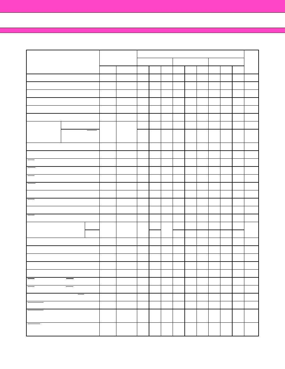
MBM29LV800TE/BE
60/70/90
30
∑ Write/Erase/Program Operations
(Continued)
Parameter
Symbol
MBM29LV800TE/BE
Unit
60
70
90
JEDEC Standard
Min Typ Max Min Typ Max Min Typ Max
Write Cycle Time
t
AVAV
t
WC
60
70
90
ns
Address Setup Time
t
AVWL
t
AS
0
0
0
ns
Address Hold Time
t
WLAX
t
AH
45
45
45
ns
Data Setup Time
t
DVWH
t
DS
30
35
45
ns
Data Hold Time
t
WHDX
t
DH
0
0
0
ns
Output Enable Setup Time
t
OES
0
0
0
ns
Output Enable
Hold Time
Read
t
OEH
0
0
0
ns
Toggle and Data
Polling
10
10
10
ns
Read Recover Time Before Write
t
GHWL
t
GHWL
0
0
0
ns
Read Recover Time Before Write
t
GHEL
t
GHEL
0
0
0
ns
CE Setup Time
t
ELWL
t
CS
0
0
0
ns
WE Setup Time
t
WLEL
t
WS
0
0
0
ns
CE Hold Time
t
WHEH
t
CH
0
0
0
ns
WE Hold Time
t
EHWH
t
WH
0
0
0
ns
Write Pulse Width
t
WLWH
t
WP
30
35
45
ns
CE Pulse Width
t
ELEH
t
CP
30
35
45
ns
Write Pulse Width High
t
WHWL
t
WPH
25
25
25
ns
CE Pulse Width High
t
EHEL
t
CPH
25
25
25
ns
Programming Operation
Byte
t
WHWH1
t
WHWH1
8
8
8
µ
s
Word
16
16
16
Sector Erase Operation *
1
t
WHWH2
t
WHWH2
1
1
1
s
V
CC
Setup Time
t
VCS
50
50
50
µ
s
Rise Time to V
ID
*
2
t
VIDR
500
500
500
ns
Voltage Transition Time *
2
t
VLHT
4
4
4
µ
s
Write Pulse Width *
2
t
WPP
100
100
100
µ
s
OE Setup Time to WE Active *
2
t
OESP
4
4
4
µ
s
CE Setup Time to WE Active *
2
t
CSP
4
4
4
µ
s
Recover Time From RY/BY
t
RB
0
0
0
ns
RESET Pulse Width
t
RP
500
500
500
ns
RESET High Level Period Before
Read
t
RH
200
200
200
ns
BYTE Switching Low to Output
High-Z
t
FLQZ
25
25
30
ns
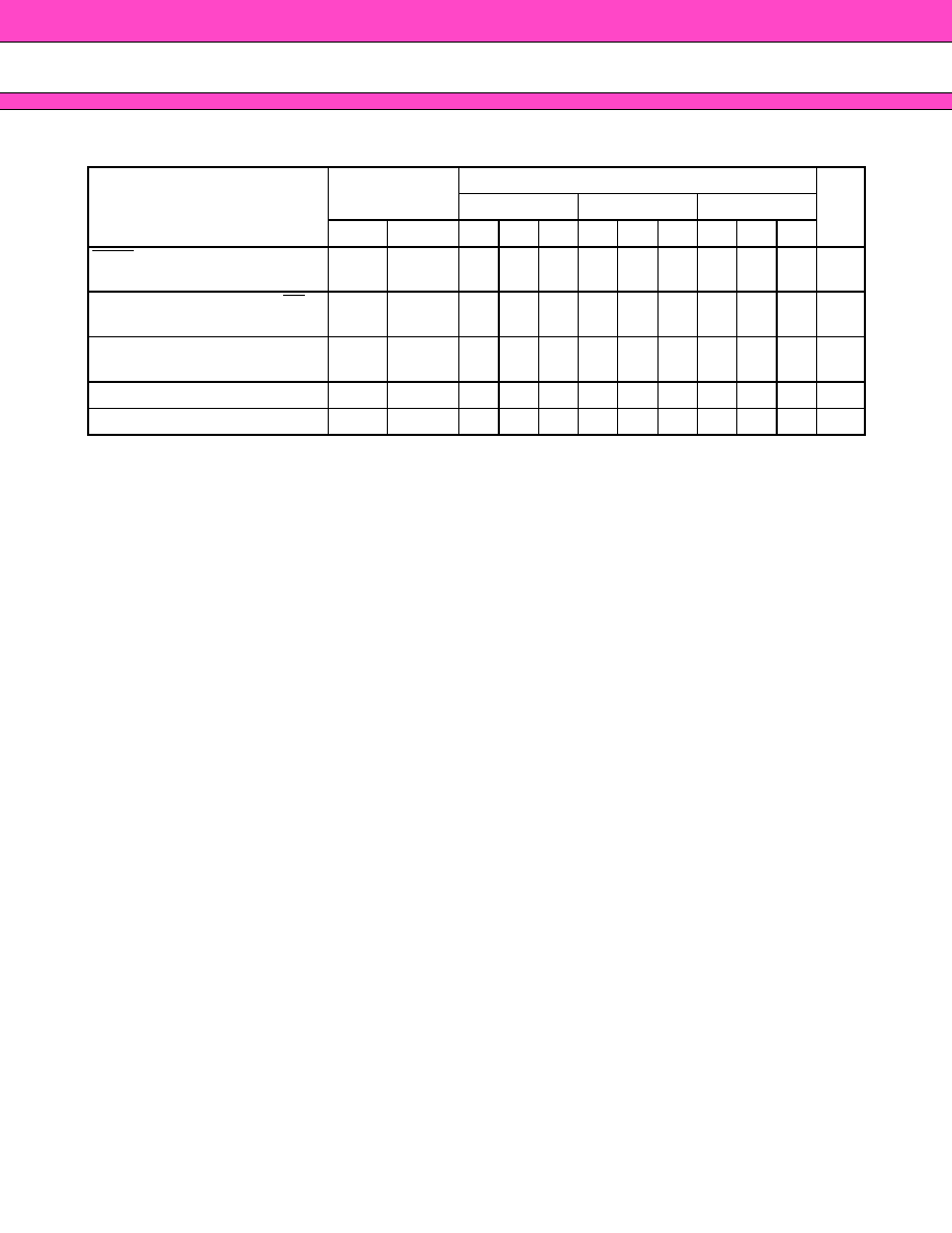
MBM29LV800TE/BE
60/70/90
31
(Continued)
*1: Does not include the preprogramming time.
*2: For Sector Protection operation.
Parameter
Symbol
MBM29LV800TE/BE
Unit
60
70
90
JEDEC Standard
Min Typ Max Min Typ Max Min Typ Max
BYTE Switching High to Output
Active
t
FHQV
60
70
90
ns
Program/Erase Valid to RY/BY
Delay
t
BUSY
90
90
90
ns
Delay Time from Embedded
Output Enable
t
EOE
60
70
90
ns
Erase Time-out Time
t
TOW
50
50
50
µ
s
Erase Suspend Transition Time
t
SPD
20
20
20
µ
s

MBM29LV800TE/BE
60/70/90
32
s
ERASE AND PROGRAMMING PERFORMANCE
s
TSOP (1) , FBGA, CSOP PIN CAPACITANCE
Notes :
∑
Test conditions T
A
=
+
25
∞
C, f
=
1.0 MHz
∑
DQ
15
/A
-1
pin capacitance is stipulated by output capacitance.
Parameter
Limits
Unit
Comments
Min
Typ
Max
Sector Erase Time
1
10
s
Excludes programming time
prior to erasure
Byte Programming Time
8
300
µ
s
Excludes system-level
overhead
Word Programming Time
16
360
Chip Programming Time
8.4
25
s
Excludes system-level
overhead
Erase/Program Cycle
100,000
cycle
Parameter
Symbol
Test Setup
Typ
Max
Unit
Input Capacitance
C
IN
V
IN
=
0
7.5
9.5
pF
Output Capacitance
C
OUT
V
OUT
=
0
8.0
10.0
pF
Control Pin Capacitance
C
IN2
V
IN
=
0
10.0
13.0
pF

MBM29LV800TE/BE
60/70/90
33
s
TIMING DIAGRAM
∑ Key to Switching Waveforms
WAVEFORM
INPUTS
OUTPUTS
Must Be
Steady
May
Change
from H to L
May
Change
from L to H
"H" or "L":
Any Change
Permitted
Does Not
Apply
Will Be
Steady
Will
Change
from H to L
Will
Change
from L to H
Changing,
State
Unknown
Center Line is
High-
Impedance
"Off" State
Address
Address Stable
High-Z
High-Z
CE
OE
WE
Outputs
Outputs Valid
t
RC
t
ACC
t
OE
t
DF
t
CE
t
OH
t
OEH
Read Operation Timing Diagram

MBM29LV800TE/BE
60/70/90
34
Address
CE
RESET
Outputs
High-Z
Outputs Valid
Address Stable
t
RC
t
ACC
t
RH
t
RP
t
RH
t
CE
t
OH
Hardware Reset/Read Operation Timing Diagram
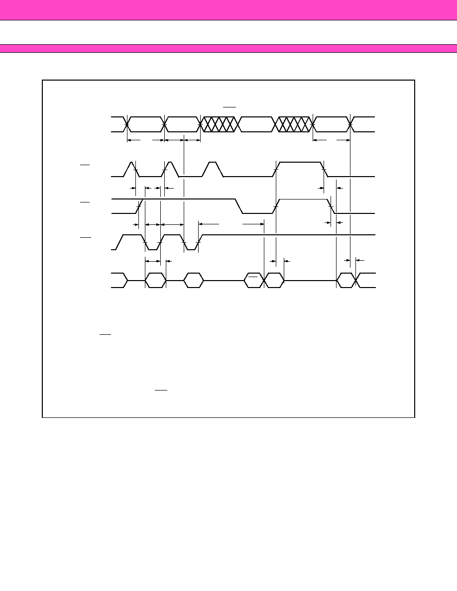
MBM29LV800TE/BE
60/70/90
35
Address
Data
CE
OE
WE
3rd Bus Cycle
Data Polling
555h
PA
A0h
PD
DQ
7
D
OUT
D
OUT
PA
t
WC
t
AS
t
AH
t
RC
t
CE
t
WHWH1
t
WPH
t
WP
t
GHWL
t
DS
t
DH
t
DF
t
OH
t
OE
t
CS
t
CH
Notes :
∑
PA is the address of the memory location to be programmed.
∑
PD is the data to be programmed at word address.
∑
DQ
7
is the output of the complement of the data written to the device.
∑
D
OUT
is the output of the data written to the device.
∑
Figure indicates the last two bus cycles out of four bus cycles sequence.
∑
These waveforms are for the
◊
16 mode (the addresses differ from
◊
8 mode).
Alternate WE Controlled Program Operation Timing Diagram

MBM29LV800TE/BE
60/70/90
36
Address
Data
WE
OE
CE
3rd Bus Cycle
Data Polling
555h
PA
A0h
PD
DQ
7
D
OUT
PA
t
WC
t
AS
t
AH
t
WHWH1
t
CPH
t
CP
t
GHEL
t
DS
t
DH
t
WS
t
WH
Alternate CE Controlled Program Operation Timing Diagram
Notes :
∑
PA is the address of the memory location to be programmed.
∑
PD is the data to be programmed at word address.
∑
DQ
7
is the output of the complement of the data written to the device.
∑
D
OUT
is the output of the data written to the device.
∑
Figure indicates the last two bus cycles out of four bus cycles sequence.
∑
These waveforms are for the
◊
16 mode (the addresses differ from
◊
8 mode) .

MBM29LV800TE/BE
60/70/90
37
Address
Data
V
CC
CE
OE
WE
555h
2AAh
555h
555h
2AAh
SA*
t
WC
t
AS
t
AH
t
CS
t
GHWL
t
CH
t
WP
t
DS
t
VCS
t
DH
t
WPH
AAh
55h
80h
AAh
55h
10h/
30h
10h for Chip Erase
Chip/Sector Erase Operation Timing Diagram
* : SA is the sector address for Sector Erase. Addresses
=
555h (Word) for Chip Erase.
Note : These waveforms are for the
◊
16 mode (the addresses differ from
◊
8 mode) .

MBM29LV800TE/BE
60/70/90
38
Data Polling during Embedded Algorithm Operation Timing Diagram
* : DQ
7
=
Valid Data (The device has completed the Embedded operation) .
t
OEH
t
CH
t
OE
t
CE
t
DF
t
BUSY
t
EOE
t
WHWH1 or
t
WHWH2
CE
DQ
7
DQ
6
to DQ
0
RY/BY
DQ
7
DQ
7
=
Valid Data
DQ
6
to DQ
0
=
Outputs Flag
DQ
6
to DQ
0
Valid Data
OE
WE
High-Z
High-Z
Data
Data
*

MBM29LV800TE/BE
60/70/90
39
t
OEH
CE
WE
t
OES
OE
DQ
6
t
OE
t
DH
Data DQ
7
to DQ
0
DQ
6
Toggle
DQ
6
Stop Toggling
DQ
6
Toggle
DQ
7
to DQ
0
Data Valid
*
Toggle Bit I during Embedded Algorithm Operation Timing Diagram
* : DQ
6
=
Stops toggling. (The device has completed the Embedded operation.)
DQ
2
vs. DQ
6
* : DQ
2
is read from the erase-suspended sector.
Enter
Embedded
Erasing
Erase
Suspend
Erase
Resume
Enter Erase
Suspend Program
Erase
Suspend
Program
Erase
Complete
Erase
Erase Suspend
Read
Erase Suspend
Read
Erase
DQ
6
DQ
2
*
WE
Toggle
DQ
2
and DQ
6
with OE or CE

MBM29LV800TE/BE
60/70/90
40
RY/BY Timing Diagram during Program/Erase Operation Timing Diagram
CE
RY/BY
WE
Rising edge of the last WE signal
t
BUSY
Entire programming
or erase operations
RESET, RY/BY Timing Diagram
t
RP
t
RB
t
READY
RY/BY
WE
RESET

MBM29LV800TE/BE
60/70/90
41
Timing Diagram for Word Mode Configuration
t
CE
t
FHQV
t
ELFH
A
-1
Data Output
(DQ
7
to DQ
0
)
Data Output
(DQ
14
to DQ
0
)
DQ
15
CE
BYTE
DQ
14
to DQ
0
DQ
15
/A
-1
t
ELFL
t
ACC
t
FLQZ
A
-1
Data Outputs
(DQ
14
to DQ
0
)
Data Outputs
(DQ
7
to DQ
0
)
DQ
15
CE
BYTE
DQ
14
to DQ
0
DQ
15
/A
-1
Timing Diagram for Byte Mode Configuration
t
AS
t
AH
CE or WE
BYTE
Input
Valid
Falling edge of last write signal
BYTE Timing Diagram for Write Operations
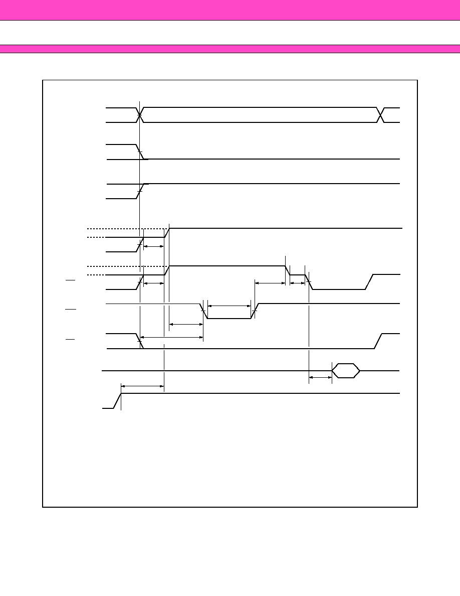
MBM29LV800TE/BE
60/70/90
42
t
WPP
t
VLHT
t
VLHT
t
OE
t
CSP
t
OESP
t
VCS
t
VLHT
t
VLHT
A
18
, A
17
, A
16
A
15
, A
14
, A
13
A
12
A
6
, A
0
A
1
A
9
V
CC
OE
V
ID
V
IH
V
ID
V
IH
WE
CE
Data
SPAX
01h
SPAY
Sector Protection Timing Diagram
SPAX : Sector Address to be protected.
SPAY : Next Sector Address to be protected.
Note : A-
1
is V
IL
on byte mode.

MBM29LV800TE/BE
60/70/90
43
Temporary Sector Unprotection Timing Diagram
Unprotection period
t
VLHT
t
VLHT
t
VCS
t
VLHT
t
VIDR
Program or Erase Command Sequence
V
CC
V
ID
V
IH
WE
RY/BY
CE
RESET

MBM29LV800TE/BE
60/70/90
44
Extended Sector Protection Timing Diagram
SPAX : Sector Address to be protected
SPAY : Next Sector Address to be protected
TIME-OUT : Time-Out window
=
150
µ
s (Min)
V
CC
WE
OE
CE
t
WC
t
WC
t
VLHT
t
VIDR
t
VCS
TIME-OUT
SPAX
SPAX
SPAY
t
WP
t
OE
60h
01h
40h
60h
60h
Data
Address
A
6
, A
0
A
1
V
ID
V
IH
RESET
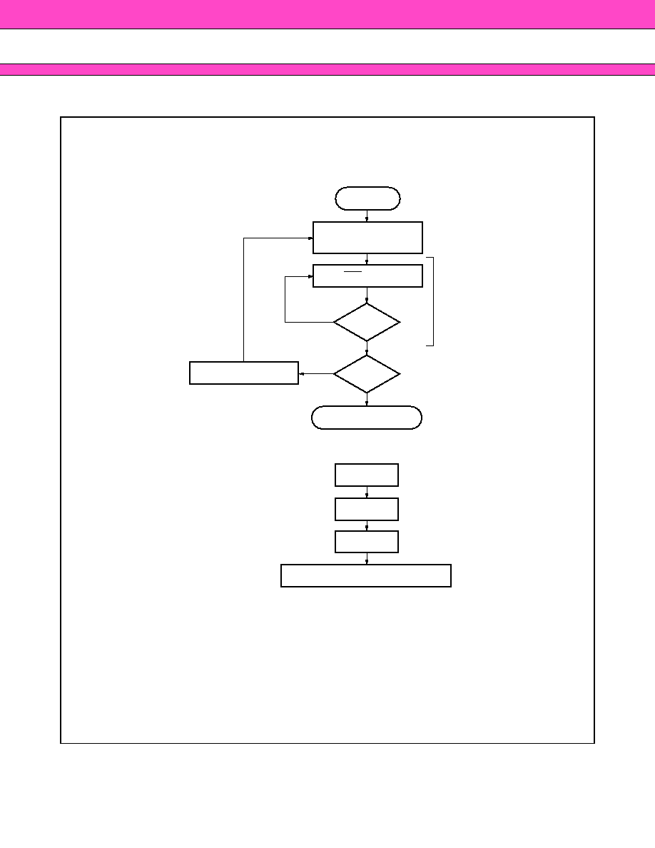
MBM29LV800TE/BE
60/70/90
45
s
FLOW CHART
Embedded Program
TM
Algorithm
Notes :
∑
The sequence is applied for
◊
16 mode.
∑
The addresses differ from
◊
8 mode.
EMBEDDED ALGORITHM
555h/AAh
555h/A0h
2AAh/55h
Program Address/Program Data
Programming Completed
Last Address
?
Increment Address
Verify Data
?
Data Polling
Program Command Sequence (Address/Command)
:
Write Program
Command Sequence
(See Below)
Start
No
No
Yes
Yes
Embedded
Program
Algorithm
in progress

MBM29LV800TE/BE
60/70/90
46
Embedded Erase
TM
Algorithm
Notes :
∑
The sequence is applied for
◊
16 mode.
∑
The addresses differ from
◊
8 mode.
EMBEDDED ALGORITHM
555h/AAh
555h/80h
2AAh/55h
555h/AAh
555h/10h
2AAh/55h
555h/AAh
555h/80h
2AAh/55h
555h/AAh
Sector Address
/30h
Sector Address
/30h
Sector Address
/30h
2AAh/55h
Erasure Completed
Data
=
FFh
?
Data Polling
Write Erase
Command Sequence
(See Below)
Start
No
Yes
Embedded
Erase
Algorithm
in progress
Chip Erase Command Sequence
(Address/Command)
:
Individual Sector/Multiple Sector
Erase Command Sequence
(Address/Command)
:
Additional sector
erase commands
are optional.
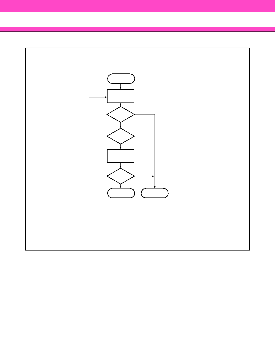
MBM29LV800TE/BE
60/70/90
47
Data Polling Algorithm
* : DQ
7
is rechecked even if DQ
5
=
"1" because DQ
7
may change simultaneously with DQ
5
.
VA
=
Address for programming
=
Any of the sector addresses
within the sector being erased
during sector erase or multiple
erases operation.
=
Any of the sector addresses
within the sector not being
protected during sector erase or
multiple sector erases
operation.
DQ
7
=
Data?
DQ
5
=
1?
Fail
Pass
DQ
7
=
Data?
*
Read Byte
(DQ
7
to DQ
0
)
Addr.
=
VA
Read Byte
(DQ
7
to DQ
0
)
Addr.
=
VA
Start
No
No
No
Yes
Yes
Yes

MBM29LV800TE/BE
60/70/90
48
Toggle Bit Algorithm
*1 : Read toggle bit twice to determine whether it is toggling.
*2 : Recheck toggle bit because it may stop toggling as DQ
5
changes to "1".
DQ
6
=
Toggle?
DQ
5
=
1?
DQ
6
=
Toggle?
Read DQ
7
to DQ
0
Addr.
=
V
IH
or V
IL
Read DQ
7
to DQ
0
Addr.
=
V
IH
or V
IL
Read DQ
7
to DQ
0
Addr.
=
V
IH
or V
IL
Start
No
No
No
Yes
Yes
Yes
*1
*1, *2
Program/Erase
Operation Not
Complete.Write
Reset Command
Program/Erase
Operation
Complete
Read DQ
7
to DQ
0
Addr.
=
V
IH
or V
IL

MBM29LV800TE/BE
60/70/90
49
Start
No
No
No
Yes
Yes
Yes
Data
=
01h?
Device Failed
PLSCNT
=
25?
PLSCNT
=
1
Remove V
ID
from A
9
Write Reset Command
Remove V
ID
from A
9
Write Reset Command
Sector Protection
Completed
Protect Another Sector
?
Increment PLSCNT
Read from Sector Address
Addr.
=
SPA, A
1
=
V
IH
A
6
=
A
0
=
V
IL
Setup Sector Addr.
A
18
, A
17
,A
16
, A
15
,
A
14
, A
13
, A
12
OE
=
V
ID
, A
9
=
V
ID
CE
=
V
IL
, RESET
=
V
IH
A
6
=
A
0
=
V
IL
, A
1
=
V
IH
Activate WE Pulse
Time out 100
µ
s
WE
=
V
IH
, CE
=
OE
=
V
IL
(A
9
should remain V
ID
)
(
)
(
)
*
Sector Protection Algorithm
* : A-
1
is V
IL
on byte mode.

MBM29LV800TE/BE
60/70/90
50
Start
Perform Erase or
Program Operations
RESET
=
V
ID
*1
RESET
=
V
IH
Temporary Sector
Unprotection Completed
*2
Temporary Sector Unprotection Algorithm
*1 : All protected sectors are unprotected.
*2 : All previously protected sectors are protected once again.

MBM29LV800TE/BE
60/70/90
51
Start
No
Yes
Yes
Data
=
01h?
PLSCNT
=
1
No
No
Yes
Device Failed
PLSCNT
=
25?
Remove V
ID
from RESET
Write Reset Command
Sector Protection
Completed
Protect Other
Group ?
Increment PLSCNT
Read from Sector Address
(Addr.
=
SPA, A
0
=
V
IL
,
A
1
=
V
IH
, A
6
=
V
IL
)
Remove V
ID
from RESET
Write Reset Command
Time out 150
µ
s
RESET
=
V
ID
Wait to 4
µ
s
No
Yes
Setup Next Sector Address
Device is Operating in
Temporary Sector
Unprotection Mode
To Protect Secter
Write 60h to Secter Address
(A
6
=
A
0
=
V
IL
, A
1
=
V
IH
)
To Verify Sector Protection
Write 40h to Secter Address
(A
6
=
A
0
=
V
IL
, A
1
=
V
IH
)
To Setup Sector Protection
Write XXXh/60h
Extended Sector
Protection Entry?
Extended Sector Protection Algorithm
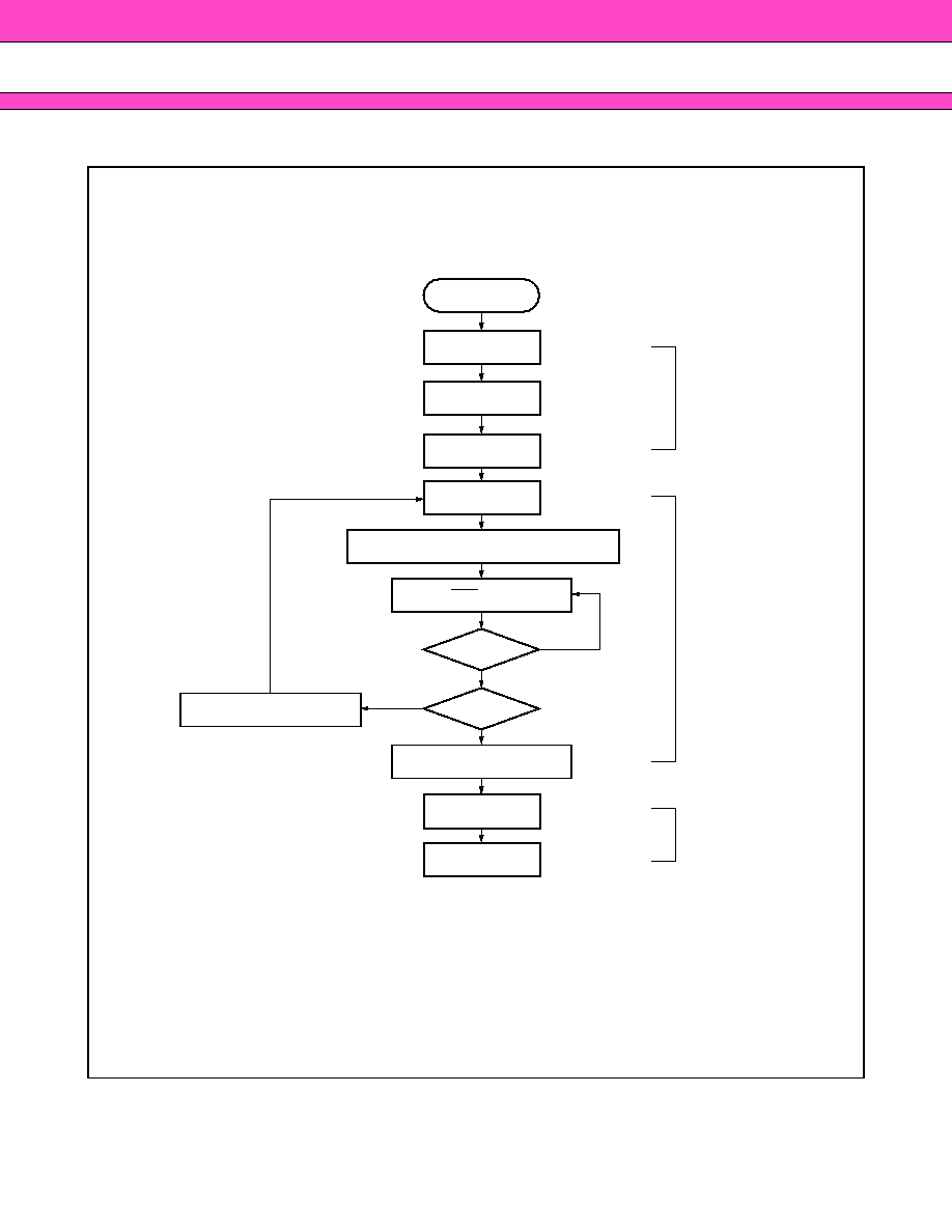
MBM29LV800TE/BE
60/70/90
52
555h/AAh
555h/20h
XXXh/90h
XXXh/F0h
XXXh/A0h
2AAh/55h
Program Address/Program Data
Programming Completed
Last Address?
Increment Address
Verify Data?
Data Polling
Start
No
No
Yes
Yes
Set Fast Mode
In Fast Program
Reset Fast Mode
Embedded Programming Algorithm for Fast Mode
Notes :
∑
The sequence is applied for
◊
16 mode.
∑
The addresses differ from
◊
8 mode.
FAST MODE ALGORITHM

MBM29LV800TE/BE
60/70/90
53
s
ORDERING INFORMATION
Part No.
Package
Access Time (ns)
Remarks
MBM29LV800TE60TN
MBM29LV800TE70TN
MBM29LV800TE90TN
48-pin plastic TSOP (1)
(FPT-48P-M19)
(Normal Bend)
60
70
90
Top Sector
MBM29LV800TE60PCV
MBM29LV800TE70PCV
MBM29LV800TE90PCV
48-pin plastic CSOP
(LCC-48P-M03)
60
70
90
MBM29LV800TE60PBT
MBM29LV800TE70PBT
MBM29LV800TE90PBT
48-ball plastic FBGA
(BGA-48P-M20)
60
70
90
MBM29LV800BE60TN
MBM29LV800BE70TN
MBM29LV800BE90TN
48-pin plastic TSOP (1)
(FPT-48P-M19)
(Normal Bend)
60
70
90
Bottom Sector
MBM29LV800BE60PCV
MBM29LV800BE70PCV
MBM29LV800BE90PCV
48-pin plastic CSOP
(LCC-48P-M03)
60
70
90
MBM29LV800BE60PBT
MBM29LV800BE70PBT
MBM29LV800BE90PBT
48-ball plastic FBGA
(BGA-48P-M20)
60
70
90
MBM29LV800
DEVICE NUMBER/DESCRIPTION
MBM29LV800
8 Mega-bit (1 M
◊
8-Bit or 512 K
◊
16-Bit) CMOS Flash Memory
3.0 V-only Read, Program, and Erase
PACKAGE TYPE
TN
=
48-Pin Thin Small Outline
Package (TSOP) Standard Pinout
PCV
=
48-Pin C-lead Small Outline
Package (CSOP)
PBT
=
48-Ball Fine Pitch Ball Grid Array
Package (FBGA)
T
E
60
PCV
SPEED OPTION
See Product Selector Guide
Device Revision
BOOT CODE SECTOR ARCHITECTURE
T
=
Top sector
B
=
Bottom sector

MBM29LV800TE/BE
60/70/90
54
s
PACKAGE DIMENSIONS
(Continued)
48-pin plastic TSOP (1)
(FPT-48P-M19)
Note 1) * : Values do not include resin protrusion.
Resin protrusion and gate protrusion are
+
0.15 (.006) Max (each side) .
Note 2) Pins width and pins thickness include plating thickness.
Note 3) Pins width do not include tie bar cutting remainder.
Dimensions in mm (inches) .
Note : The values in parentheses are reference values.
≠
.003
+.001
≠
0.08
+0.03
.007
0.17
"A"
(Stand off height)
0.10(.004)
(Mounting
height)
(.472±.008)
12.00
±0.20
LEAD No.
48
25
24
1
(.004
±.002)
0.10(.004)
M
1.10
+0.10
≠
0.05
+.004
≠
.002
.043
0.10
±0.05
(.009
±.002)
0.22
±0.05
(.787
±.008)
20.00
±0.20
(.724
±.008)
18.40
±0.20
INDEX
2003 FUJITSU LIMITED F48029S-c-6-7
C
0~8
∞
0.25(.010)
0.50(.020)
0.60
±0.15
(.024
±.006)
Details of "A" part
*
*

MBM29LV800TE/BE
60/70/90
55
(Continued)
48-pin plastic CSOP
(LCC-48P-M03)
Note 1) *1 : Resin protrusion. (Each side :
+
0.15 (.006) Max) .
Note 2) *2 : These dimensions do not include resin protrusion.
Note 3) Pins width includes plating thickness.
Note 4) Pins width do not include tie bar cutting remainder.
Dimensions in mm (inches) .
Note : The values in parentheses are reference values.
C
2003 FUJITSU LIMITED C48056S-c-2-2
10.00±0.10(.394±.004)
0.08(.003)
9.20(.362)REF
1
24
25
48
INDEX
INDEX
9.50±0.10
(.374±.004)
10.00±0.20
(.394±.008)
"A"
0.22±0.035
(.009±.001)
.002
≠.0
+.002
≠0
+0.05
0.05
0.95±0.05(.037±.002)
(Mounting height)
(Stand off)
0.65(.026)
1.15(.045)
Details of "A" part
0∞~10∞
LEAD No.
*
2
*
1
0.40(.016)
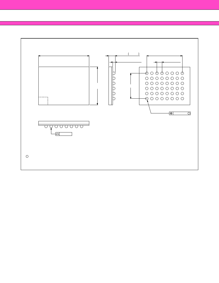
MBM29LV800TE/BE
60/70/90
56
(Continued)
48-ball plastic FBGA
(BGA-48P-M20)
Dimensions in mm (inches) .
Note : The values in parentheses are reference values.
C
2003 FUJITSU LIMITED B48020S-c-2-2
8.00
±0.20(.315±.008)
0.38
±0.10(.015±.004)
(Stand off)
(Mounting height)
6.00
±0.20
(.236
±.008)
0.10(.004)
0.80(.031)TYP
5.60(.220)
4.00(.157)
48-¯0.45±0.05
(48-¯.018
±.002)
M
¯0.08(.003)
H
G
F
E
D
C
B
A
6
5
4
3
2
1
.043
≠.005
+.003
≠0.13
+0.12
1.08
(INDEX AREA)

MBM29LV800TE/BE
60/70/90
FUJITSU LIMITED
All Rights Reserved.
The contents of this document are subject to change without notice.
Customers are advised to consult with FUJITSU sales
representatives before ordering.
The information, such as descriptions of function and application
circuit examples, in this document are presented solely for the
purpose of reference to show examples of operations and uses of
Fujitsu semiconductor device; Fujitsu does not warrant proper
operation of the device with respect to use based on such
information. When you develop equipment incorporating the
device based on such information, you must assume any
responsibility arising out of such use of the information. Fujitsu
assumes no liability for any damages whatsoever arising out of
the use of the information.
Any information in this document, including descriptions of
function and schematic diagrams, shall not be construed as license
of the use or exercise of any intellectual property right, such as
patent right or copyright, or any other right of Fujitsu or any third
party or does Fujitsu warrant non-infringement of any third-party's
intellectual property right or other right by using such information.
Fujitsu assumes no liability for any infringement of the intellectual
property rights or other rights of third parties which would result
from the use of information contained herein.
The products described in this document are designed, developed
and manufactured as contemplated for general use, including
without limitation, ordinary industrial use, general office use,
personal use, and household use, but are not designed, developed
and manufactured as contemplated (1) for use accompanying fatal
risks or dangers that, unless extremely high safety is secured, could
have a serious effect to the public, and could lead directly to death,
personal injury, severe physical damage or other loss (i.e., nuclear
reaction control in nuclear facility, aircraft flight control, air traffic
control, mass transport control, medical life support system, missile
launch control in weapon system), or (2) for use requiring
extremely high reliability (i.e., submersible repeater and artificial
satellite).
Please note that Fujitsu will not be liable against you and/or any
third party for any claims or damages arising in connection with
above-mentioned uses of the products.
Any semiconductor devices have an inherent chance of failure. You
must protect against injury, damage or loss from such failures by
incorporating safety design measures into your facility and
equipment such as redundancy, fire protection, and prevention of
over-current levels and other abnormal operating conditions.
If any products described in this document represent goods or
technologies subject to certain restrictions on export under the
Foreign Exchange and Foreign Trade Law of Japan, the prior
authorization by Japanese government will be required for export
of those products from Japan.
F0405
©
FUJITSU LIMITED Printed in Japan