
DS07-12552-1E
FUJITSU SEMICONDUCTOR
DATA SHEET
8-bit Proprietary Microcontroller
CMOS
F
2
MC-8L MB89470 Series
MB89475/P475/PV470
s
DESCRIPTION
The MB89470 series has been developed as a general-purpose version of the F
2
MC*-8L family consisting of
proprietary 8-bit, single-chip microcontrollers.
In addition to a compact instruction set, the microcontroller contains a variety of peripheral functions such as 21-
bit time-base timer, watch prescaler, PWC timer, PWM timer, 8/16-bit timer/counter, external interrupt 1 (edge) ,
external interrupt 2 (level) , 10-bit A/D converter, UART/SIO, buzzer, watchdog timer reset.
The MB89470 series is designed suitable for home appliance as well as in a wide range of applications for
consumer product.
* : F
2
MC stands for FUJITSU Flexible Microcontroller.
s
FEATURES
∑ Package used
QFP package, LQFP package and SH-DIP package for MB89P475, MB89475
MQFP package for MB89PV470
(Continued)
s
PACKAGES
48-pin Plastic SH-DIP
48-pin Plastic LQFP
48-pin Plastic QFP
48-pin Ceramic MQFP
(DIP-48P-M01)
(FPT-48P-M05)
(FPT-48P-M13)
(MQP-48C-P01)

MB89470 Series
2
(Continued)
∑ High-speed operating capability at low voltage
∑ Minimum execution time : 0.32
µ
s/12.5 MHz
∑ F
2
MC-8L family CPU core
∑ Six timers
PWC timer (also usable as an interval timer)
PWM timer
8/16-bit timer/counter
◊
2
21-bit timebase timer
Watch prescaler
∑ Buzzer
7 frequency types are selectable by software
∑ External interrupts
Edge detection (Selectable edge) : 4 channels
Low-level interrupt (Wake-up function) : 5 channels
∑ A/D converter (8 channels)
10-bit successive approximation type
∑ UART/SIO
Synchronous/asynchronous data transfer capable
∑ Low-power consumption modes
Stop mode (Oscillation stops to minimize the current consumption.)
Sleep mode (The CPU stops to reduce the current consumption to approx. 1/3 of normal.)
Subclock mode (for dual clock product)
Watch mode (for dual clock product)
∑ Watch dog timer reset
∑ I/O ports : Max 39 channels
Multiplication and division instructions
Instruction set optimized for controllers
16-bit arithmetic operations
Bit test and branch instructions
Bit manipulation instructions, etc.

MB89470 Series
3
s
PRODUCT LINEUP
(Continued)
Part number
Parameter
MB89475
MB89P475
MB89PV470
Classification
Mass production products
(mask ROM product)
OTP
Piggy-back
ROM size
16 K
◊
8-bit (internal ROM)
16 K
◊
8-bit (internal PROM,
can be written to by FLASH
programmer)
32 K
◊
8-bit (external ROM)
RAM size
512
◊
8 bits
1 K
◊
8 bits
CPU functions
Number of instructions
Instruction bit length
Instruction length
Data bit length
Minimum execution time
Minimum interrupt processing time
: 136
: 8 bits
: 1 to 3 bytes
: 1, 8, 16 bits
: 0.32
µ
s/12.5 MHz
: 2.88
µ
s/12.5 MHz
Ports
Output-only ports (N-channel open drain)
Input-only ports
I/O ports (CMOS)
Total
: 7 pins
: 3 pins (1 pin in product with
dual clock)
: 29 pins
: 39 pins
21-bit Time-base
timer
Interrupt period (0.82 ms, 3.3 ms, 26.2 ms, 419.4 ms) at 10 MHz
Interrupt period (0.66 ms, 2.6 ms, 21.0 ms, 335.5 ms) at 12.5 MHz
Watchdog timer
Reset period (209.7 ms to 419.4 ms) at 10 MHz
Reset period (167.8 ms to 335.5 ms) at 12.5 MHz
Watch prescaler
17 bits
Interrupt cycle : 31.25 ms, 0.25 ms, 0.5 s, 1.00 s, 2.00 s, 4.00 s/32.768 kHz for subclock
Pulse width count
timer
2 channels
8-bit one-shot timer operation (supports underflow output, operating clock period : 1, 4, 32
t
inst
*, external)
8-bit reload timer operation (supports square wave output, operating clock period : 1, 4,
32 t
inst
*, external)
8-bit pulse width measurement operation (supports continuous measurement, H width, L
width, rising edge to rising edge, falling edge to falling edge measurement and both edge
measurement)
PWM timer
8-bit reload timer operation (supports square wave output, operating clock period : 1, 4,
32 t
inst
*, external)
8-bit resolution PWM operation
8/16-bit timer/
counter 1, 2
Can be operated either as a 2-channel 8-bit timer/counter (Timer 1 and Timer 2, each with
its own independent operating clock cycle) , or as one 16-bit timer/counter
In Timer 1 or 16-bit timer/counter operation, event counter operation (external clock-trig-
gered) and square wave output capable
8/16-bit timer/
counter 3, 4
Can be operated either as a 2-channel 8-bit timer/counter (Timer 3 and Timer 4, each with
its own independent operating clock cycle) , or as one 16-bit timer/counter
In Timer 3 or 16-bit timer/counter operation, event counter operation (external clock-trig-
gered) and square wave output capable
External interrupt
4 independent channels (selectable edge, interrupt vector, request flag)
5 channels (low level interrupt)
MB89470 Series
4
(Continued)
* : t
inst
is one instruction cycle (execution time) , which can be selected as 1/4, 1/8, 1/16, or 1/64 of main clock.
s
PACKAGE AND CORRESPONDING PRODUCTS
O : Available
X : Not available
s
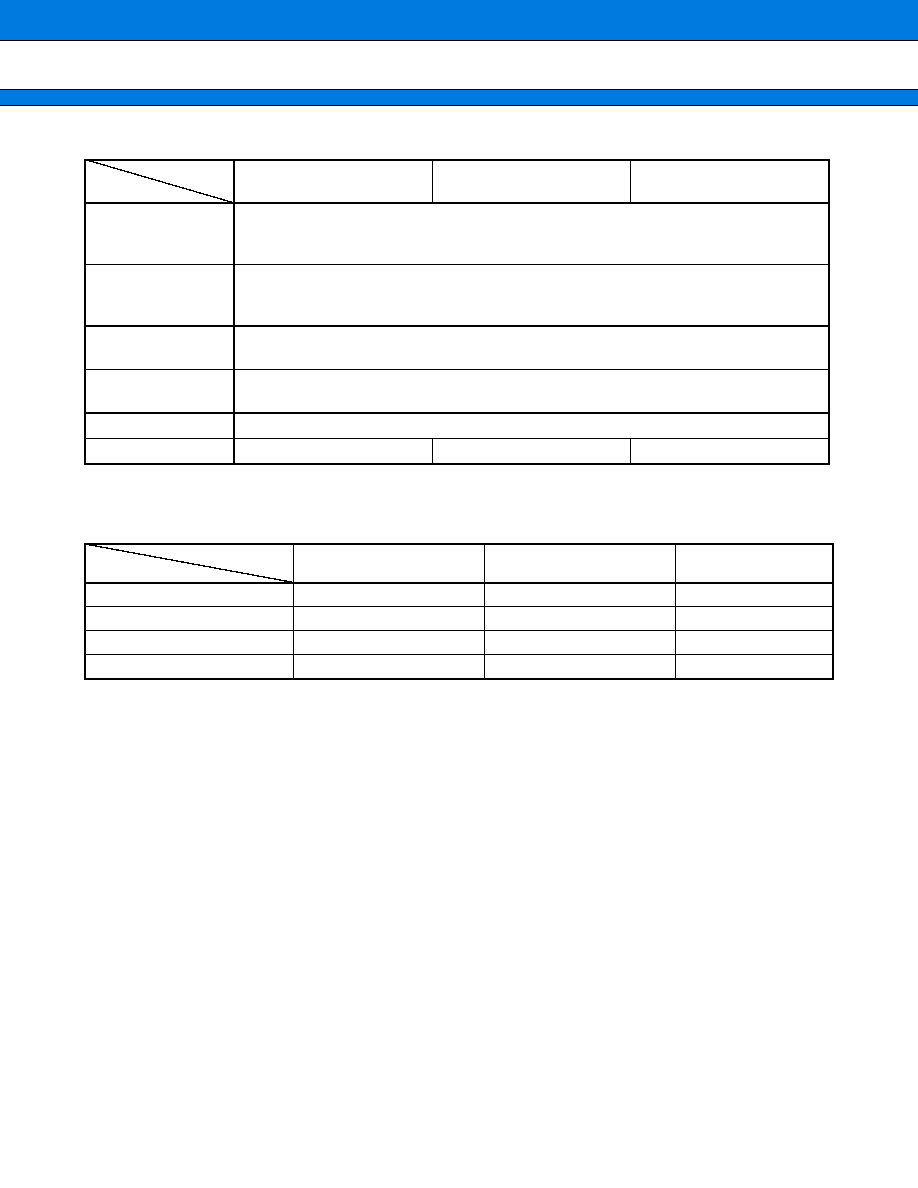
DIFFERENCES AMONG PRODUCTS
1.
Memory Size
Before evaluating using the piggyback product, verify its differences from the product that will actually be used.
Take particular care on the following point :
∑ The stack area, etc., is set at the upper limit of the RAM.
2.
Current Consumption
∑ For the MB89PV470, add the current consumed by the EPROM mounted in the piggy-back socket.
∑ When operating at low speed, the current consumed by the one-time PROM product is greater than that for
the mask ROM product. However, the current consumption are roughly the same in sleep or stop mode.
∑ For more information, see "
s
ELECTRICAL CHARACTERISTICS".
3.
Oscillation stabilization time after power-on reset
∑ For MB89PV470, there is no power-on stabilization time after power-on reset.
∑ For MB89P475, there is power-on stabilization time after power-on reset.
∑ For MB89475, the power-on stabilization time can be select.
∑ For more information, refer to "
s
MASK OPTIONS".
Part number
Parameter
MB89475
MB89P475
MB89PV470
A/D converter
10-bit resolution
◊
8 channels
A/D conversion function (conversion time : 60 t
inst
*)
Supports repeated activation by internal clock.
UART/SIO
Synchronous/asynchronous data transfer capable
(Max baud rate : 78.125 Kbps at 10 MHz)
(7 and 8 bits with parity bit ; 8 and 9 bits without parity bit)
Buzzer output
7 frequency types (F
CH
/2
12
, F
CH
/2
11
, F
CH
/2
10
, F
CH
/2
9
, F
CL
/2
5
, F
CL
/2
4
, F
CL
/2
3
) are selectable by
software.
Standby mode
Sleep mode, stop mode, subclock mode (dual clock product) and watch mode (dual clock
product)
Process CMOS
Operating Voltage
2.2 V to 5.5 V
3.5 V to 5.5 V
2.7 V to 5.5 V
Part number
Package
MB89475
MB89P475
MB89PV470
DIP-48P-M01
O
O
X
FPT-48P-M05
O
O
X
FPT-48P-M13
O
O
X
MQP-48C-P01
X
X
O

MB89470 Series
5
s
PIN ASSIGNMENTS
(Continued)
(TOP VIEW)
(DIP-48P-M01)
*1 : For pin no. 2, connect this pin to an external 0.1
µ
F capacitor to ground (for MB89P475 only) .
For MB89PV470 and MB89475, this pin should be left unconnected.
*2 : High current drive type
V
SS
C*
1
P40/X0A
P41/X1A
P17/TO2
P16/EC2
P15/TO1
P14/EC1
P13/INT13
P12/INT12
P11/INT11
P10/INT10
P07/AN7
P06/AN6
P05/AN5
P04/AN4
P03/AN3
P02/AN2
P01/AN1
P00/AN0
AV
SS
AV
CC
P54/INT24
P53/INT23
1
2
3
4
5
6
7
8
9
10
11
12
13
14
15
16
17
18
19
20
21
22
23
24
48
47
46
45
44
43
42
41
40
39
38
37
36
35
34
33
32
31
30
29
28
27
26
25
X1
X0
MODE
P42
RST
P20/SCK1
P21/SO1
P22/SI1
P23/PWC
P24/PWM
P25/SI2
V
CC
P26/SO2
P27/SCK2
P30/BUZ*
2
P31*
2
P32*
2
P33*
2
P34*
2
P35*
2
P36*
2
P50/INT20
P51/INT21
P52/INT22

MB89470 Series
6
(Continued)
(TOP VIEW)
(FPT-48P-M05)
(FPT-48P-M13)
*1 : For pin no. 20, connect this pin to an external 0.1
µ
F capacitor to ground (for MB89P475 only) .
For MB89PV470 and MB89475, this pin should be left unconnected.
*2 : High current drive type
1
2
3
4
5
6
7
8
9
10
11
12
P33*
2
P32*
2
P31*
2
P30/BUZ*
2
P27/SCK2
P26/SO2
V
CC
P25/SI2
P24/PWM
P23/PWC
P22/SI1
P21/SO1
36
35
34
33
32
31
30
29
28
27
26
25
P02/AN2
P03/AN3
P04/AN4
P05/AN5
P06/AN6
P07/AN7
P10/INT10
P11/INT11
P12/INT12
P13/INT13
P14/EC1
P15/TO1
48
47
46
45
44
43
42
41
40
39
38
37
P34
*
2
P35
*
2
P36
*
2
P50/INT20
P51/INT21
P52/INT22
P53/INT23
P54/INT24
AV
CC
AV
SS
P00/AN0
P01/AN1
13
14
15
16
17
18
19
20
21
22
23
24
P20/SCK1
RST
P42
MODE
X0
X1
V
SS
C
*
1
P40/X0A
P41/X1A
P17/TO2
P16/EC2

MB89470 Series
7
(Continued)
(TOP VIEW)
(MQP-48C-P01)
*1 : Package upper-side pin assignment ( MB89PV470 only)
N.C. : As connected internally, do not use.
*2 : Pin no. 20 should be left unconnected.
*3 : High current drive type
Pin no.
Pin name
Pin no.
Pin name
Pin no.
Pin name
Pin no.
Pin name
49
V
pp
57
N.C.
65
O4
73
OE
50
A12
58
A2
66
O5
74
N.C.
51
A7
59
A1
67
O6
75
A11
52
A6
60
A0
68
O7
76
A9
53
A5
61
O1
69
O8
77
A8
54
A4
62
O2
70
CE
78
A13
55
A3
63
O3
71
A10
79
A14
56
N.C.
64
V
ss
72
N.C.
80
Vcc
1
2
3
4
5
6
7
8
9
10
11
12
36
35
34
33
32
31
30
29
28
27
26
25
48
47
46
45
44
43
42
41
40
39
38
37
13
14
15
16
17
18
19
20
21
22
23
24
69
70
71
72
73
74
75
76
60
59
58
57
56
55
54
53
68
67
66
65
64
63
62
61
77
78
79
80
49
50
51
52
P33*
3
P32*
3
P31*
3
P30/BUZ*
3
P27/SCK2
P26/SO2
V
CC
P25/SI2
P24/PWM
P23/PWC
P22/SI1
P21/SO1
P02/AN2
P03/AN3
P04/AN4
P05/AN5
P06/AN6
P07/AN7
P10/INT10
P11/INT11
P12/INT12
P13/INT13
P14/EC1
P15/TO1
P34
*
3
P35
*
3
P36
*
3
P50/INT20
P51/INT21
P52/INT22
P53/INT23
P54/INT24
AV
CC
AV
SS
P00/AN0
P01/AN1
P20/SCK1
RST
P42
MODE
X0
X1
V
SS
C
*
2
P40/X0A
P41/X1A
P17/TO2
P16/EC2
*1

MB89470 Series
8
s
PIN DESCRIPTION
(Continued)
Pin no.
Pin name
I/O
circuit
Function
LQFP/QFP/
MQFP*
2
SDIP*
1
17
47
X0
A
Connection pins for a crystal or other oscillator.
An external clock can be connected to X0. In this case, leave X1
open.
18
48
X1
16
46
MODE
B
Input pins for setting the memory access mode.
Connect directly to V
SS
.
14
44
RST
C
Reset I/O pin. The pin is a N-ch open-drain type with pull-up resistor
and a hysteresis input. The pin outputs an "L" level when an internal
reset request is present. Inputting an "L" level initializes internal cir-
cuits.
38 to 31
20 to 13
P00/AN0 to
P07/AN7
D
General-purpose I/O port.
The pins are shared with the analog inputs for the A/D converter.
30 to 27
12 to 9
P10/INT10
to
P13/INT13
E
General-purpose I/O port.
A hysteresis input for INT10 to INT13.
The pin is shared with an external interrupt 1 input.
26
8
P14/EC1
E
General-purpose I/O port.
A hysteresis input for EC1.
The pin is shared with the 8/16 bit timer 1 input.
25
7
P15/TO1
F
General-purpose I/O port.
The pin is shared with the output of 8/16-bit timer 1.
24
6
P16/EC2
E
General-purpose I/O port.
A hysteresis input for EC2.
The pin is shared with the 8/16 bit timer 2 input.
23
5
P17/TO2
F
General-purpose I/O port.
The pin is shared with the output of 8/16-bit timer 2.
13
43
P20/SCK1
E
General-purpose I/O port.
A hysteresis input for SCK1.
The pin is shared with the clock I/O of UART/SIO 1.
12
42
P21/SO1
F
General-purpose I/O port.
The pin is shared with the serial data output of UART/SIO 1.
11
41
P22/SI1
E
General-purpose I/O port.
A hysteresis input for SI1.
The pin is shared with the serial data input of UART/SIO 1.
10
40
P23/PWC
E
General-purpose I/O port.
A hysteresis input for PWC.
This pin is shared with PWC input.
9
39
P24/PWM
F
General-purpose input port.
This pin is shared with PWM output.
8
38
P25/SI2
E
General-purpose I/O port.
A hysteresis input for SI2.
The pin is shared with the serial data input of UART/SIO 2.

MB89470 Series
9
(Continued)
*1 : DIP-48P-M01
*2 : FPT-48P-M05/FPT-48P-M13/MQP-48C-P01
*3 : When MB89475 or MB89PV470 is used, this pin will become a N.C. pin without internal connection.
When MB89P475 is used, connect this pin to an external 0.1
µ
F capacitor to ground.
Pin no.
Pin name
I/O
circuit
Function
LQFP/QFP/
MQFP*
2
SDIP*
1
6
36
P26/SO2
F
General-purpose I/O port.
The pin is shared with the serial data output of UART/SIO 2.
5
35
P27/SCK2
E
General-purpose I/O port.
A hysteresis input for SCK2.
The pin is shared with the clock I/O of UART/SIO 2.
4
34
P30/BUZ
G
N-channel open-drain output.
The pin is shared with buzzer output.
3 to 1,
48 to 46
33 to
28
P31 to P36
G
N-channel open-drain output.
21
3
P40/X0A
H
General-purpose input port. (single clock system)
A
Connection pins for a crystal or other oscillator. (dual clock system)
An external clock can be connected to X0A. In this case, leave X1A
open.
22
4
P41/X1A
H
General-purpose input port. (single clock system)
A
Connection pins for a crystal or other oscillator. (dual clock system)
An external clock can be connected to X0A. In this case, leave X1A
open.
15
45
P42
H
General-purpose input port.
45 to 41
27 to
23
P50/INT20
to
P54/INT24
E
General-purpose I/O port.
A hysteresis input for INT20 to INT24.
The pin is shared with an external interrupt 2 input.
20
2
C
Capacitor connection pin
*3
7
37
V
CC
Power supply pin (
+
5 V) .
19
1 V
SS
Power supply pin (GND) .
40
22
AV
CC
A/D converter power supply pin.
39
21
AV
SS
A/D converter power supply pin.
Use at the same voltage level as V
SS
.

MB89470 Series
10
∑ External EPROM Socket (MB89PV470 only)
* : MQP-48C-P01
Pin no.
Pin
name
I/O
Function
MQFP*
49
V
pp
O
"H" level output pin
50
51
52
53
54
55
58
59
60
A12
A7
A6
A5
A4
A3
A2
A1
A0
O
Address output pins.
61
62
63
O1
O2
O3
I
Data input pins.
64
V
SS
O
Power supply pin (GND) .
65
66
67
68
69
O4
O5
O6
O7
O8
I
Data input pins.
70
CE
O
Chip enable pin for the ROM. Outputs "H" in standby mode.
71
A10
O
Address output pin.
73
OE
O
Output enable pin for the ROM. Always outputs "L".
75
76
77
78
79
A11
A9
A8
A13
A14
O
Address output pins.
80
V
CC
O
Power supply pin for the EPROM.
56
57
72
74
N.C.
Internally connected pins. Always leave open.

MB89470 Series
11
s
I/O CIRCUIT TYPE
(Continued)
Type
Circuit
Remarks
A
∑ Main and sub-clock circuits
∑ Oscillation feedback resistance
is approx. 500 k
for main clock
circuit and 5 M
for sub-clock cir-
cuit.
B
∑ Hysteresis input
∑ The pull-down resistor is
approx. 50 k
.
(No pull-down resistor in
MB89P475)
C
∑ The pull-up resistance (P-chan-
nel) is approx. 50 k
.
∑ Hysteresis input
D
∑ CMOS output
∑ CMOS input
∑ Selectable pull-up resistor
Approx. 50 k
E
∑ CMOS output
∑ CMOS input
∑ Selectable pull-up resistor
Approx. 50 k
X1 (X1A)
X0 (X0A)
Nch Pch
Pch
Nch
Stop mode control signal
Pch
Nch
R
Pch
Nch
R
pull-up
resistor register
ADIN
Pch
Nch
pull-up
resistor register
resources
port
R
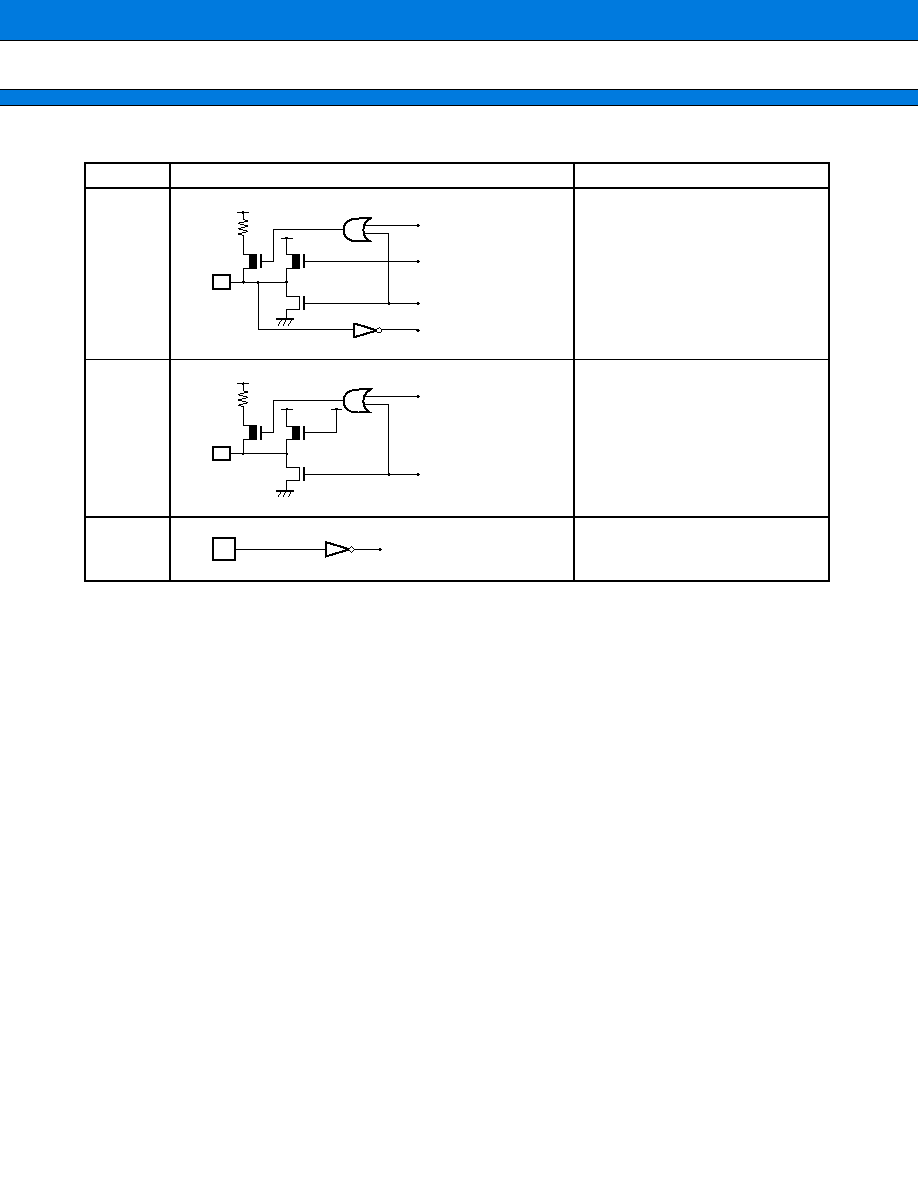
MB89470 Series
12
(Continued)
Type
Circuit
Remarks
F
∑ CMOS output
∑ CMOS input
∑ Selectable pull-up resistor
Approx. 50 k
G
∑ N-channel open-drain output
∑ Selectable pull-up resistor
Approx. 50 k
H
∑ CMOS input
Pch
Nch
pull-up
resistor regsiter
R
Pch
Nch
pull-up
resistor register
R
port

MB89470 Series
13
s
HANDLING DEVICES
1.
Preventing Latchup
Latchup may occur on CMOS ICs if voltage higher than V
CC
or lower than V
SS
is applied to input and output pins
other than medium- to high-voltage pins or if higher than the voltage which shows on "1. Absolute Maximum
Ratings" in "
s
ELECTRICAL CHARACTERISTICS" is applied between V
CC
and V
SS
.
When latchup occurs, power supply current increases rapidly and might thermally damage elements. When
using, take great care not to exceed the absolute maximum ratings.
Also, take care to prevent the analog power supply (AV
CC
) and analog input from exceeding the digital power
supply (V
CC
) when the analog system power supply is turned on and off.
2.
Treatment of Unused Input Pins
Leaving unused input pins open could cause malfunctions. They should be connected to a pull-up or pull-down
resistor.
3.
Treatment of Power Supply Pins on Microcontrollers with A/D Converter
Connect to be AV
CC
=
V
CC
and AV
SS
=
V
SS
even if the A/D converter is not in use.
4.
Treatment of N.C. Pins
Be sure to leave (internally connected) N.C. pins open.
5.
Power Supply Voltage Fluctuations
Although V
CC
power supply voltage is assured to operate within the rated range, a rapid fluctuation of the voltage
could cause malfunctions, even if it occurs within the rated range. Stabilizing voltage supplied to the IC is therefore
important. As stabilization guidelines, it is recommended to control power so that V
CC
ripple fluctuations (P-P
value) will be less than 10
%
of the standard V
CC
value at the commercial frequency (50 Hz to 60 Hz) and the
transient fluctuation rate will be less than 0.1 V/ms at the time of a momentary fluctuation such as when power
is switched.
6.
Precautions when Using an External Clock
Even when an external clock is used, oscillation stabilization time is required for power-on reset (optional) and
wake-up from stop mode.
7.
Note to noise in the External Reset Pin (RST)
If the reset pulse applied to the external reset pin (RST) does not meet the specifications, it may cause malfunc-
tions. Use causion so that the reset pulse less than the specifications will not be fed to the external reset pin (RST).

MB89470 Series
14
s
PROGRAMMING OTPROM IN MB89P475 WITH SERIAL PROGRAMMER
1.
Programming the OTPROM with serial programmer
∑ All OTP products can be programmed with serial programmer.
2.
Programming the OTPROM
∑ To program the OTPROM using FUJITSU MCU programmer MB91919-001.
Inquiry : Fujitsu Microelectronics Asia Pte Ltd. : TEL (65) -2810770
FAX (65) -2810220
3.
Programming Adapter for OTPROM
∑ To program the OTPROM using FUJITSU MCU programmer MB91919-001, use the programming adapter
listed below.
Inquiry : Fujitsu Microelectronics Asia Pte Ltd. : TEL (65) -2810770
FAX (65) -2810220
4.
OTPROM Content Protection
For product with OTPROM content protection feature (MB89P475-102, MB89P475-202) , OTPROM content can
be read using serial programmer if the OTPROM content protection mechanism is not activated.
One predefined area of the OTPROM (FFFC
H
) is assigned to be used for preventing the read access of OTPROM
content. If the protection code "00
H
" is written in this address (FFFC
H
) , the OTPROM content cannot be read
by any serial programmer.
Note : The program written into the OTPROM cannot be verified once the OTPROM protection code is written ("00
H
"
in FFFC
H
) . It is advised to write the OTPROM protection code at last.
5.
Programming Yield
All bits cannot be programmed at Fujitsu shipping test to a blanked OTPROM microcomputer, due to its nature.
For this reason, a programming yield of 100
%
cannot be assured at all times.
Package
Compatible socket adapter
DIP-48P-M01
MB91919-805
+
MB91919-800
FPT-48P-M05
MB91919-806
+
MB91919-800
FPT-48P-M13
MB91919-807
+
MB91919-800

MB89470 Series
15
s
PROGRAMMING OTPROM IN MB89P475 WITH PROGRAMMER
1.
Programming OTPROM with parallel programmer
∑ Only products without protection feature (i.e. MB89P475-101 and MB89P475-201) can be programmed with
parallel programmer. Product with protection feature (i.e. MB89P475-102 and MB89P475-202) cannot be
programmed with parallel programmer.
2.
ROM Writer Adapters and Recommended ROM Writers
∑ The following shows ROM writer adapters and recommended ROM writers.
Ando Electric Co., Ltd. (Parallel programmer)
* : For the version of the programmer, contact the Flash Support Group, Inc.
Fujitsu Microelectronics Asia Pte Ltd. (Serial programmer)
Inquiries : Fujitsu Microelectronics Asia Pte Ltd. : TEL (65) -2810770
Sunhayato Corp.
: TEL 81-(3)-3984-7791
FAX 81-(3)-3971-0535
E-mail : adapter@sunhayato.co.jp
Flash Support Group, Inc
: FAX 81-(53)-428-8377
E-mail : support@j-fsg.co.jp
3.
Writing data to the OTPROM
(1) Set the OTPROM writer for the CU50-OTP (device code : cdB6DC) .
(2) Load the program data to the OTPROM writer.
(3) Write data using the OTPROM writer.
4.
Programming Yield
All bits cannot be programmed at Fujitsu shipping test to a blanked OTPROM microcomputer, due to its nature.
For this reason, a programming yield of 100
%
cannot be assured at all times.
Package
Applicable adapter model
Recommended writer
DIP-48P-M01
ROM2-48SD-32DP-8LA
AF9708*
AF9709*
AF9723*
FPT-48P-M05
ROM2-48LQF-32DP-8LA2
FPT-48P-M13
ROM2-48QF-32DP-8LA2
Package
Applicable adapter model
Recommended writer
DIP-48P-M01
MB91919-601
MB91919-001
FPT-48P-M05
MB91919-602
FPT-48P-M13
MB91919-603

MB89470 Series
16
s
PROGRAMMING TO THE EPROM WITH PIGGYBACK/EVALUATION DEVICE
1.
EPROM for Use
MBM27C256A-20TVM
2.
Programming Socket Adapter
To program to the PROM using an EPROM programmer, use the socket adapter (manufacturer : Sunhayato
Corp.) listed below.
Inquiry : Sunhayato Corp. : TEL 81-(3)-3984-7791
FAX 81-(3)-3971-0535
E-mail : adapter@sunhayato.co.jp
3.
Memory Space
Memory space in each mode is diagrammed below.
4.
Programming to the EPROM
(1) Set the EPROM programmer to the MBM27C256.
(2) Load program data into the EPROM programmer at 0000
H
to 7FFF
H
.
(3) Program to 0000
H
to 7FFF
H
with the EPROM programmer.
Package
Adapter socket part number
LCC-32
(Square) ROM-32LC-28DP-S
0000
H
7FFF
H
0000
H
RAM
Not available
PROM
32 KB
EPROM
32 KB
I/O
0080
H
FFFF
H
8000
H
0880
H
Address
Normal operating
mode
Corresponding addresses on
the EPROM programmer

MB89470 Series
17
s
BLOCK DIAGRAM
*1 : High Current Pins
*2 : Unconnected pin for MB89PV470 and MB89475
*3 : P40, P41 pins for single-clock system and X01A, X1A pins for dual-clock system
X0
Oscillator
Clock Controller
Sub-clock
Oscillator
Reset circuit
(Watchdog timer)
21-bit Time-base
timer
External interrupt 2
(Level)
External interrupt 1
(Level)
8/16-bit Timer 1, 2
UART/SIO 1
UART/SIO 2
Buzzer
8-bit PWC
8-bit PWM
8/16-bit Timer 3, 4
Watch Prescaler
Internal data bus
5
5
CMOS Input port 4
CMOS I/O port 0
P00/AN0
to P07/AN7
AV
CC
AV
SS
P10/INT10 to P13/INT13
P14/EC1
P15/TO1
P16/EC2
P20/SCK1
P21/SO1
P22/SI1
P23/PWC
P24/PWM
P25/SI2
P26/SO2
P27/SCK2
P30/BUZ
*1
P31
*1
to P36
*1
P17/TO2
8
8
4
4
CMOS I/O port 1
CMOS I/O port 2
N-ch open-drain output port 3
6
10-bit
A/D converter
CMOS I/O port 5
1 Kbyte RAM/512 Byte RAM
16 Kbyte ROM
Other pins
MODE, V
CC
, V
SS
, C
*2
F
2
MC-8L
CPU
X1
P40/X0A*
3
P41/X1A*
3
P42
P50/INT20 to
P54/INT24
RST
MB89470 Series
18
s
CPU CORE
1.
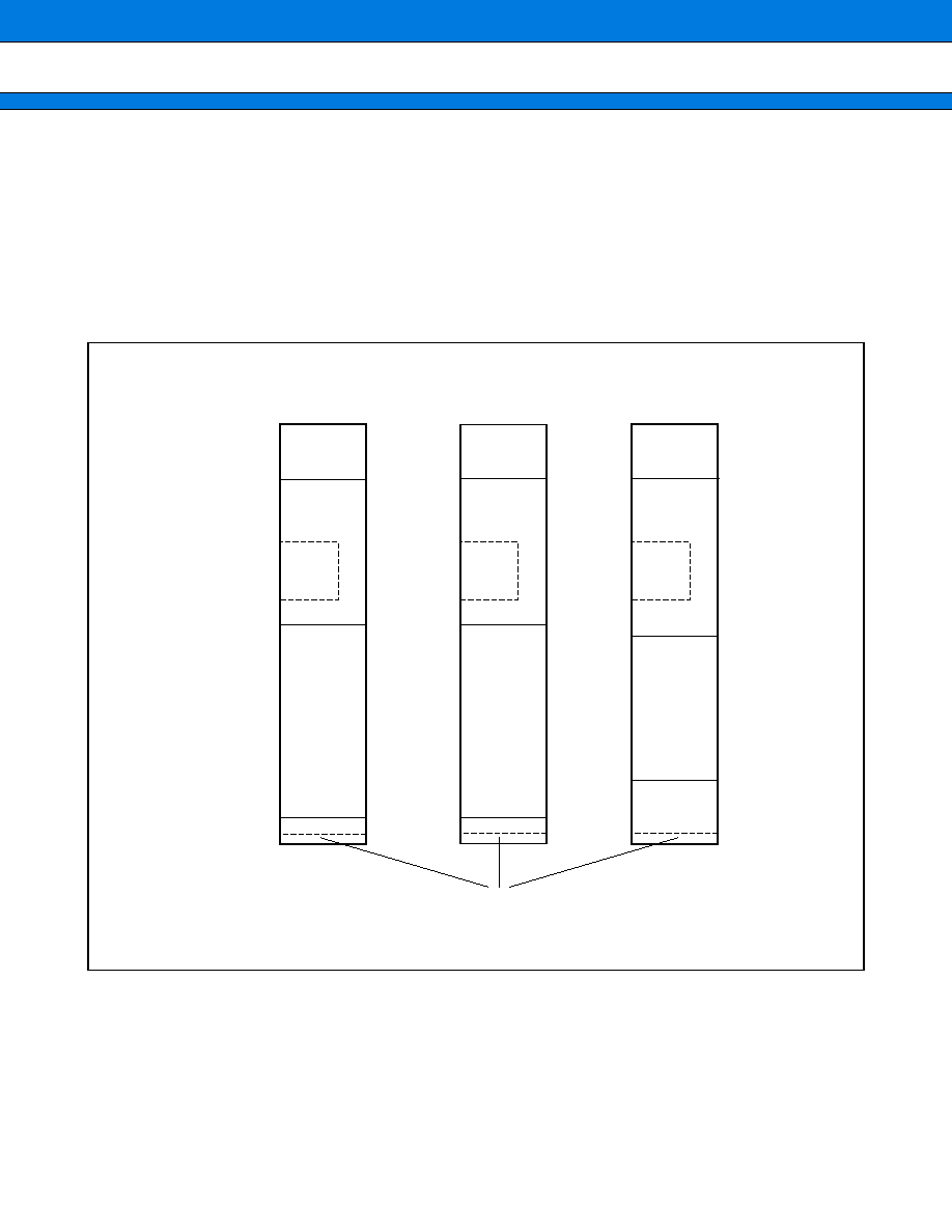
Memory Space
The microcontrollers of the MB89470 series offer a memory space of 64 Kbytes for storing all of I/O, data, and
program areas. The I/O area is located at the lowest address. The data area is provided immediately above the
I/O area. The data area can be divided into register, stack, and direct areas according to the application. The
program area is located at exactly the opposite end, that is, near the highest address. Provide the tables of
interrupt reset vectors and vector call instructions toward the highest address within the program area. The
memory space of the MB89470 series is structured as illustrated below.
0000
H
0080
H
0100
H
MB89PV470
I/O
RAM
Vacant
External
ROM
(32 K)
0000
H
0080
H
0100
H
0200
H
C000
H
C000
H
8000
H
FFFF
H
I/O
RAM
Vacant
FFFF
H
0280
H
0280
H
0200
H
0480
H
FFC0
H
FFC0
H
0000
H
0080
H
0100
H
MB89P475
MB89475
I/O
RAM
Vacant
Vector table (reset, interrupt, vector call instruction)
ROM
ROM
FFFF
H
0200
H
FFC0
H
General-
purpose
registers
General-
purpose
registers
General-
purpose
registers
Memory Map

MB89470 Series
19
2.
Registers
The F
2
MC-8L family has two types of registers; dedicated registers in the CPU and general-purpose registers
in the memory. The following registers are provided :
The PS can further be divided into higher 8 bits for use as a register bank pointer (RP) and the lower 8 bits for
use as a condition code register (CCR) . (See the diagram below.)
Program counter (PC)
: A 16-bit register for indicating instruction storage positions
Accumulator (A)
: A 16-bit temporary register for storing arithmetic operations, etc. When the
instruction is an 8-bit data processing instruction, the lower byte is used.
Temporary accumulator (T) : A 16-bit register which performs arithmetic operations with the accumulator.
When the instruction is an 8-bit data processing instruction, the lower byte is
used.
Index register (IX)
: A 16-bit register for index modification
Extra pointer (EP)
: A 16-bit pointer for indicating a memory address
Stack pointer (SP)
: A 16-bit register for indicating a stack area
Program status (PS)
: A 16-bit register for storing a register pointer, a condition code
PC
A
T
IX
EP
SP
PS
: Program counter
: Accumulator
: Temporary accumulator
: Index register
: Extra pointer
: Stack pointer
: Program status
16 bits
FFFD
H
Undefined
Undefined
Undefined
Undefined
Undefined
I-flag = 0, IL1, 0 = 11
Other bits are undefined.
Initial value
PS
RP
CCR
15
14
13
12
11
10
9
8
7
6
5
4
3
2
1
0
RP
Vacancy Vacancy Vacancy
H
I
IL1, 0
N
Z
V
C
Structure of the Program Status Register

MB89470 Series
20
The RP indicates the address of the register bank currently in use. The relationship between the pointer contents
and the actual address is based on the conversion rule illustrated below.
The CCR consists of bits indicating the results of arithmetic operations and the contents of transfer data and
bits for control of CPU operations at the time of an interrupt.
H-flag : Set when a carry or a borrow from bit 3 to bit 4 occurs as a result of an arithmetic operation. Cleared
otherwise. This flag is for decimal adjustment instructions.
I-flag :
Interrupt is allowed when this flag is set to 1. Interrupt is prohibited when the flag is set to 0. Set to 0
when reset.
IL1, 0 :
Indicates the level of the interrupt currently allowed. Processes an interrupt only if its request level is
higher than the value indicated by this bit.
IL1
IL0
Interrupt level
High-low
0
0
1
High
Low
=
no interrupt
0
1
1
0
2
1
1
3
N-flag : Set if the MSB is set to 1 as the result of an arithmetic operation. Cleared when the bit is set to 0.
Z-flag : Set when an arithmetic operation results in 0. Cleared otherwise.
V-flag : Set if the complement on 2 overflows as a result of an arithmetic operation. Reset if the overflow does
not occur.
C-flag : Set when a carry or a borrow from bit 7 occurs as a result of an arithmetic operation. Cleared other-
wise. Set to the shift-out vallue in the case of a shift instruction.
"0"
"0"
"0"
"0"
"0"
"0"
"0"
"1"
R4
R3
R2
R1
R0
b2
b1
RP
Lower OP codes
b0
A7
A6
A5
A4
A3
A2
A1
A0
A15
Generated addresses
A14 A13 A12 A11 A10
A9
A8
Rule for Conversion of Actual Addresses of the General-purpose Register Area

MB89470 Series
21
The following general-purpose registers are provided :
General-purpose registers : An 8-bit resister for storing data
The general-purpose registers are 8 bits and located in the register banks of the memory. One bank contains
eight registers. Up to a total of 32 banks can be used on the MB89470 series. The bank currently in use is
indicated by the register bank pointer (RP) .
R0
This address = 0100
H
+
8
◊
(RP)
R1
R2
R3
R4
R5
R6
R7
Memory area
32 banks
Register Bank Configuration

MB89470 Series
22
s
I/O MAP
(Continued)
Address
Register name
Register Description
Read/Write
Initial value
00
H
PDR0
Port 0 data register
R/W
XXXXXXXX
B
01
H
DDR0
Port 0 data direction register
W*
00000000
B
02
H
PDR1
Port 1 data register
R/W
XXXXXXXX
B
03
H
DDR1
Port 1 data direction register
W*
00000000
B
04
H
PDR2
Port 2 data register
R/W
00000000
B
05
H
(Reserved)
06
H
DDR2
Port 2 data direction register
R/W
00000000
B
07
H
SYCC
System clock control register
R/W
-XXMM-00
B
08
H
STBC
Standby control register
R/W
0001XXXX
B
09
H
WDTC
Watchdog timer control register
W*
0---XXXX
B
0A
H
TBTC
Timebase timer control register
R/W
00---000
B
0B
H
WPCR
Watch prescaler control register
R/W
00--0000
B
0C
H
PDR3
Port 3 data register
R/W
-1111111
B
0D
H
PDR4
Port 4 data register
R
-----XXX
B
0E
H
RSFR
Reset flag register
R
XXXX----
B
0F
H
BUZR
Buzzer register
R/W
-----000
B
10
H
PDR5
Port 5 data register
R/W
---XXXXX
B
11
H
DDR5
Port 5 data direction register
R/W
---00000
B
12
H
, 13
H
(Reserved)
14
H
T4CR
Timer 4 control register
R/W
000000X0
B
15
H
T3CR
Timer 3 control register
R/W
000000X0
B
16
H
T4DR
Timer 4 data register
R/W
XXXXXXXX
B
17
H
T3DR
Timer 3 data register
R/W
XXXXXXXX
B
18
H
T2CR
Timer 2 control register
R/W
000000X0
B
19
H
T1CR
Timer 1 control register
R/W
000000X0
B
1A
H
T2DR
Timer 2 data register
R/W
XXXXXXXX
B
1B
H
T1DR
Timer 1 data register
R/W
XXXXXXXX
B
1C
H
to 1F
H
(Reserved)
20
H
ADC1
A/D control register 1
R/W
-00000X0
B
21
H
ADC2
A/D control register 2
R/W
-0000001
B
22
H
ADDH
A/D data register (Upper byte)
R
------XX
B
23
H
ADDL
A/D data register (Lower byte)
R
XXXXXXXX
B
24
H
ADER
A/D input enable register
R/W
11111111
B
25
H
(Reserved)
26
H
SMC11
UART/SIO serial mode control register 11
R/W
00000000
B

MB89470 Series
23
(Continued)
* : Bit manipulation instruction cannot be used.
Address
Register name
Register Description
Read/Write
Initial value
27
H
SMC12
UART/SIO serial mode control register 12
R/W
00000000
B
28
H
SSD1
UART/SIO serial status and data register 1
R
00001---
B
29
H
SIDR1/SODR1
UART/SIO serial data register 1
R/W *
XXXXXXXX
B
2A
H
SRC1
UART/SIO serial rate control register 1
R/W
XXXXXXXX
B
2B
H
SMC21
UART serial mode control register 21
R/W
00000000
B
2C
H
SMC22
UART serial mode control register 22
R/W
00000000
B
2D
H
SSD2
UART serial status and data register 2
R
00001---
B
2E
H
SIDR2/SODR2
UART serial data register 2
R/W *
XXXXXXXX
B
2F
H
SRC2
UART serial rate control register 2
R/W
XXXXXXXX
B
30
H
EIC1
External interrupt 1 control register 1
R/W
00000000
B
31
H
EIC2
External interrupt 1 control register 2
R/W
00000000
B
32
H
EIE2
External interrupt 2 enable register
R/W
---00000
B
33
H
EIF2
External interrupt 2 flag register
R/W
-------0
B
34
H
PCR1
PWC control register 1
R/W
0-0--000
B
35
H
PCR2
PWC control register 2
R/W
00000000
B
36
H
PLBR
PWC reload buffer register
R/W
XXXXXXXX
B
37
H
(Reserved)
38
H
CNTR
PWM timer control register
R/W
0-00000000
B
39
H
COMR
PWM timer compare register
W*
XXXXXXXX
B
3A
H
to 6F
H
(Reserved)
70
H
PURC0
Port 0 pull up resistor control register
R/W
11111111
B
71
H
PURC1
Port 1 pull up resistor control register
R/W
11111111
B
72
H
PURC2
Port 2 pull up resistor control register
R/W
11111111
B
73
H
PURC3
Port 3 pull up resistor control register
R/W
-1111111
B
74
H
(Reserved)
75
H
PURC5
Port 5 pull up resistor control register
R/W
---1111
B
76
H
to 7A
H
(Reserved)
7B
H
ILR1
Interrupt level setting register 1
W*
11111111
B
7C
H
ILR2
Interrupt level setting register 2
W*
11111111
B
7D
H
ILR3
Interrupt level setting register 3
W*
11111111
B
7E
H
ILR4
Interrupt level setting register 4
W*
11111111
B
7F
H
(Reserved)

MB89470 Series
24
∑ Read/write access symbols
∑ Initial value symbols
R/W : Readable and writable
R
: Read-only
W
: Write-only
0
: The initial value of this bit is "0".
1
: The initial value of this bit is "1".
X
: The initial value of this bit is undefined.
-
: Unused bit.
M
: The initial value of this bit is determined by mask option.

MB89470 Series
25
s
ELECTRICAL CHARACTERISTICS
1.
Absolute Maximum Ratings
(AV
SS
=
V
SS
=
0.0 V)
WARNING: Semiconductor devices can be permanently damaged by application of stress (voltage, current,
temperature, etc.) in excess of absolute maximum ratings. Do not exceed these ratings.
Parameter
Symbol
Value
Unit
Remarks
Min
Max
Power supply voltage
V
CC
AV
CC
V
SS
-
0.3
V
SS
+
6.0
V
AV
CC
must not exceed V
CC
Input voltage
V
I
V
SS
-
0.3
V
CC
+
0.3
V
Output voltage
V
O
V
SS
-
0.3
V
CC
+
0.3
V
"L" level maximum output current
I
OL
15
mA
"L" level average output current
I
OLAV1
4
mA
Average value (operating current
◊
operating rate)
P00 to P07, P10 to P17,
P20 to P27, P50 to P54, RST
I
OLAV2
12
mA
Average value (operating current
◊
operating rate)
P30 to P36
"L" level total maximum output
current
I
OL
100
mA
"L" level total average output
current
I
OLAV
40
mA
Average value (operating current
◊
operating rate)
"H" level maximum output current
I
OH
-
15
mA
"H" level average output current
I
OHAV
-
2
mA
Average value (operating current
◊
operating rate)
"H" level total maximum output
current
I
OH
-
50
mA
"H" level total average output
current
I
OHAV
-
20
mA
Average value (operating current
◊
operating rate)
Power consumption
P
D
300
mW
Operating temperature
T
A
-
40
+
85
∞
C
Storage temperature
Tstg
-
55
+
150
∞
C

MB89470 Series
26
2.
Recommended Operating Conditions
(AV
SS
=
V
SS
=
0.0 V)
* : These values depend on the operating conditions and the analog assurance range. See "Operating Voltage vs.
Main Clock Operating Frequency" and "5. A/D Converter Electrical Characteristics."
Parameter
Symbol
Value
Unit
Remarks
Min
Max
Power supply voltage
V
CC
AV
CC
2.2*
5.5
V
Operation assurance
range
MB89475
3.5*
5.5
V
Operation assurance
range
MB89P475
2.7*
5.5
V
Operation assurance
range
MB89PV470
1.5
5.5
V
Retains the RAM state in
stop mode
Operating temperature
T
A
-
40
+
85
∞
C

MB89470 Series
27
Operating Voltage vs. Main Clock Operating Frequency
"Operating Voltage vs. Main Clock Operating Frequency" indicates the operating frequency of the external oscilla-
tor at an instruction cycle of 4/F
CH
.
Since the operating voltage range is dependent on the instruction cycle, see minimum execution time if the oper-
ating speed is switched using a gear.
WARNING: The recommended operating conditions are required in order to ensure the normal operation of the
semiconductor device. All of the device's electrical characteristics are warranted when the device is
operated within these ranges.
Always use semiconductor devices within their recommended operating condition ranges. Operation
outside these ranges may adversely affect reliability and could result in device failure.
No warranty is made with respect to uses, operating conditions, or combinations not represented on
the data sheet. Users considering application outside the listed conditions are advised to contact their
FUJITSU representatives beforehand.
5.5
5.0
4.5
4.0
3.5
3.0
2.0
2.7
2.2
1.0
Note :
This area is not assured for MB89P475.
This area is not assured for MB89PV470 and MB89P475.
2.0
3.0
4.0
5.0
6.0
7.0
8.0
9.0
10.0
11.0
12.0
4.0
2.0
1.33
1.0
0.8
0.66
0.57
0.50
0.44
0.4
0.36
0.33
12.5
0.32
Operating
Voltage (V)
Analog accuracy
assurance range :
V
CC
= AV
CC
= 4.5 V to 5.5 V
Main clock
operating Freq. (MHz)
Min execution
time (inst. cycle) (
µ
s)

MB89470 Series
28
3.
DC Characteristics
(AV
CC
=
V
CC
=
5.0 V, AV
SS
=
V
SS
=
0.0 V, T
A
=
-
40
∞
C to
+
85
∞
C)
(Continued)
Parameter
Symbol
Pin
Condition
Value
Unit
Remarks
Min
Typ
Max
"H" level
input voltage
V
IH
P00 to P07,
P10 to P17,
P20 to P27,
P40 to P42,
P50 to P54
0.7 V
CC
V
CC
+
0.3
V
V
IHS
RST, MODE, EC1,
EC2, SCK1, SI1,
SCK2, SI2, PWC,
INT10 to INT13,
INT20 to INT24
0.8 V
CC
V
CC
+
0.3
V
"L" level
input voltage
V
IL
P00 to P07,
P10 to P17,
P20 to P27,
P40 to P42,
P50 to P54
V
SS
-
0.3
0.3 V
CC
V
V
ILS
RST, MODE, EC1,
EC2, SCK1, SI1,
SCK2, SI2, PWC,
INT10 to INT13,
INT20 to INT24
V
SS
-
0.3
0.2 V
CC
V
Open-drain
output pin
application
voltage
V
D
P30 to P36
V
SS
-
0.3
V
CC
+
0.3
V
"H" level
output
voltage
V
OH
P00 to P07,
P10 to P17,
P20 to P27,
P50 to P54
I
OH
=
-
2.0 mA
4.0
V
"L" level
output
voltage
V
OL1
P00 to P07,
P10 to P17,
P20 to P27,
P50 to P54, RST
I
OL
=
4.0 mA
0.4
V
V
OL2
P30 to P36
I
OL
=
12.0 mA
0.4
V
Input leak-
age current
I
LI
P00 to P07,
P10 to P17,
P20 to P27,
P50 to P54
0.45 V
<
V
I
<
V
CC
-
5
+
5
µ
A
Without
pull-up
resistor
Open drain
output
leakage
current
I
LOD
P30 to P36
0.45 V
<
V
I
<
V
CC
-
5
+
5
µ
A

MB89470 Series
29
(Continued)
(AV
CC
=
V
CC
=
5.0 V, AV
SS
=
V
SS
=
0.0 V, T
A
=
-
40
∞
C to
+
85
∞
C)
Parameter
Symbol
Pin
Condition
Value
Unit
Remarks
Min
Typ
Max
Pull-down
resistance
R
DOWN
MODE
V
I
=
V
CC
25
50
100
k
Except
MB89P475
Pull-up
resistance
R
PULL
P00 to P07,
P10 to P17,
P20 to P27,
P30 to P36,
P50 to P54, RST
V
I
=
0.0 V
25
50
100
k
When pull-up
resistor is
selected (ex-
cept RST)
Power
supply
current
I
CC1
V
CC
F
CH
=
12.5 MHz
t
inst
=
0.32
µ
s
Main clock
run mode
7
13
mA
I
CC2
F
CH
=
12.5 MHz
t
inst
=
5.12
µ
s
Main clock
run mode
1
3
mA
I
CCS1
F
CH
=
12.5 MHz
t
inst
=
0.32
µ
s
Main clock
sleep mode
2.5
5
mA
I
CCS2
F
CH
=
12.5 MHz
t
inst
=
5.12
µ
s
Main clock
sleep mode
0.7
2
mA
I
CCL
F
CL
=
32.768 kHz
Subclock mode
37
85
µ
A
MB89PV470
MB89475
350
785
µ
A
MB89P475
I
CCLS
F
CL
=
32.768 kHz
Subclock sleep
mode
11
30
µ
A
I
CCT
F
CL
=
32.768 kHz
Watch mode
Main clock
stop mode
1.4
15
µ
A
MB89PV470
MB89475
5.6
21
µ
A
MB89P475
I
CCH
Ta
=
+
25
∞
C
Subclock stop
mode
1
10
µ
A
I
A
AV
cc
F
CH
=
12.5 MHz
2.8
6
mA
A/D
converting
I
AH
Ta
=
+
25
∞
C
1
5
µ
A
A/D stop
Input
capacitance
C
IN
Other than V
CC
,
V
SS
, AV
CC
, AV
SS
f
=
1 MHz
5
15
pF
MB89470 Series
30
4.
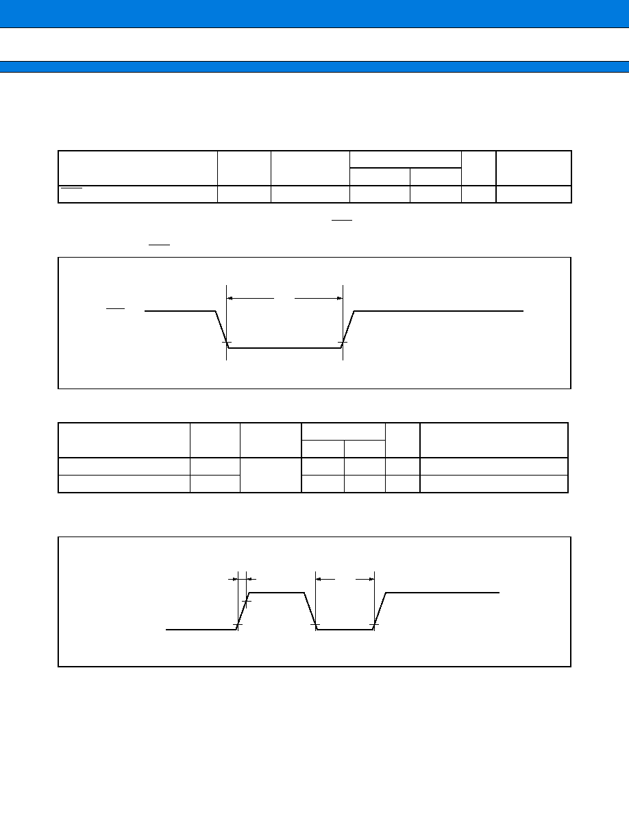
AC Characteristics
(1) Reset Timing
(V
CC
=
5.0 V, AV
SS
=
V
SS
=
0.0 V, T
A
=
-
40
∞
C to
+
85
∞
C)
Notes :
∑
t
HCYL
is the oscillation cycle (1/F
C
) to input to the X0 pin.
∑
If the reset pulse applied to the external reset pin (RST) does not meet the specifications, it may cause
malfunctions. Use caution so that the reset pulse less than the specifications will not be fed to the external
reset pin (RST).
(2) Power-on Reset
(AV
SS
=
V
SS
=
0.0 V, T
A
=
-
40
∞
C to
+
85
∞
C)
Note : Make sure that power supply rises within the selected oscillation stabilization time.
Rapid changes in power supply voltage may cause a power-on reset. If power supply voltage needs to be
varied in the course of operation, a smooth voltage rise is recommended.
Parameter
Symbol
Condition
Value
Unit
Remarks
Min
Max
RST "L" pulse width
t
ZLZH
48 t
HCYL
ns
Parameter
Symbol
Condition
Value
Unit
Remarks
Min
Max
Power supply rising time
t
R
50
ms
Power supply cut-off time
t
OFF
1
ms
Due to repeated operations
0.2 V
CC
0.2 V
CC
t
ZLZH
RST
0.2 V
3.5 V
0.2 V
0.2 V
t
OFF
V
CC
t
R
MB89470 Series
31
(3) Clock Timing
(AV
SS
=
V
SS
=
0.0 V, T
A
=
-
40
∞
C to
+
85
∞
C)
Parameter
Symbol
Pin
Value
Unit
Remarks
Min
Typ
Max
Clock frequency
F
CH
X0, X1
1
12.5
MHz
F
CL
X0A, X1A
32.768
kHz
Clock cycle time
t
HCYL
X0, X1
80
1000
ns
t
LCYL
X0A, X1A
30.5
µ
s
Input clock pulse width
P
WH
P
WL
X0
20
ns
External clock
P
WHL
P
WLL
X0A
15.2
µ
s
Input clock rising/falling time
t
CR
t
CF
X0, X0A
10
ns
0.2 V
CC
0.2 V
CC
0.8 V
CC
0.8 V
CC
0.2 V
CC
P
WH
t
HCYL
t
CR
t
CF
P
WL
X0
X 0
X 1
C1
C2
F
CH
When a crystal
or
ceramic oscillator is used
Open
When an external clock is used
F
CH
X 0
X 1
X0 and X1 Timing and Conditions
Main Clock Conditions

MB89470 Series
32
(4) Instruction Cycle
Parameter
Symbol
Value
Unit
Remarks
Instruction cycle
(minimum execution time)
t
inst
4/F
CH
, 8/F
CH
, 16/F
CH
, 64/F
CH
µ
s
(4/F
CH
) t
inst
=
0.32
µ
s when operating
at F
CH
=
12.5 MHz
2/F
CL
µ
s
t
inst
=
61.036
µ
s when operating at
F
CL
=
32.768 kHz
X 0 A
X 1 A
C
0
C
1
Rd
Open
When a crystal
or
ceramic oscillator is used
When sub-clock is not used in dual clock product
X 0 A
X 1 A
F
CL
Open
When an external clock is used
F
CL
X 0 A
X 1 A
0.8
V
CC
t
LCYL
0.2
V
CC
P
WHL
P
WLL
t
CF
t
CR
X0A
Subclock Timing and Conditions
Subclock Conditions

MB89470 Series
33
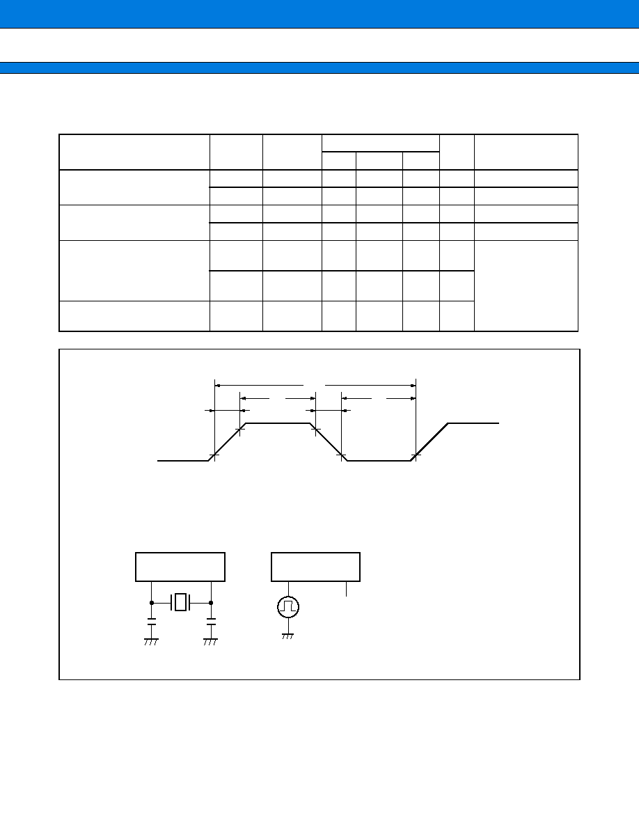
(5) Serial I/O Timing
(V
CC
=
5.0 V, AV
SS
=
V
SS
=
0.0 V, T
A
=
-
40
∞
C to
+
85
∞
C)
* : For information on t
inst
, see " (4) Instruction Cycle."
Parameter
Symbol
Pin
Condition
Value
Unit
Min
Max
Serial clock cycle time
t
SCYC
SCK1, SCK2
Internal shift
clock mode
2 t
inst
*
µ
s
SCK
SO time
t
SLOV
SCK1, SO1, SCK2, SO2,
-
200
+
200
ns
Valid SI
SCK
t
IVSH
SI1, SCK1, SI2, SCK2
1/2 t
inst
*
ns
SCK
valid SI hold time
t
SHIX
SCK1, SI1, SCK2, SI2
1/2 t
inst
*
ns
Serial clock "H" pulse width
t
SHSL
SCK1, SCK2
External
shift clock
mode
1 t
inst
*
µ
s
Serial clock "L" pulse width
t
SLSH
1 t
inst
*
µ
s
SCK
SO time
t
SLOV
SCK1, SO1, SCK2, SO2
0
200
ns
Valid SI
SCK
t
IVSH
SI1, SCK1, SI2, SCK2
1/2 t
inst
*
ns
SCK
valid SI hold time
t
SHIX
SCK1, SI1, SCK2, SI2
1/2 t
inst
*
ns
0.8 V
2.4 V
2.4 V
0.8 V
CC
0.2 V
CC
0.8 V
t
SCYC
t
SLOV
t
IVSH
t
SHIX
SCK
SO
SI
0.8 V
0.8 V
CC
0.2 V
CC
0.2 V
CC
0.2 V
CC
2.4 V
0.8 V
CC
0.8 V
CC
0.8 V
CC
0.2 V
CC
t
SLSH
t
SHSL
t
SLOV
t
IVSH
t
SHIX
SCK
SO
SI
0.8 V
0.8 V
CC
0.2 V
CC
Internal Clock Operation
External Clock Operation

MB89470 Series
34
(6) Peripheral Input Timing
(AV
CC
=
V
CC
=
5.0 V, AV
SS
=
V
SS
=
0.0 V, T
A
=
-
40
∞
C to
+
85
∞
C)
* : For information on t
inst
, see " (4) Instruction Cycle."
Parameter
Symbol
Pin
Value
Unit
Remarks
Min
Max
Peripheral input "H" pulse width 1
t
ILIH1
INT10 to INT13,
INT20 to INT24, EC1,
EC2, PWC
2 t
inst
*
µ
s
Peripheral input "L" pulse width 1
t
IHIL1
2 t
inst
*
µ
s
0.2 V
CC
0.8 V
CC
t
IHIL1
0.8 V
CC
INT10 to INT13,
INT20 to INT24,
EC1, EC2,
PWC
0.2 V
CC
t
ILIH1

MB89470 Series
35
5.
A/D Converter Electrical Characteristics
(1) A/D Converter Electrical Characteristics
(AV
CC
=
V
CC
=
4.5 V to 5.5 V, AV
SS
=
V
SS
=
0.0 V, T
A
=
-
40
∞
C to
+
85
∞
C)
* : For information on t
inst
, see " (4) Instruction Cycle" in "4. AC Characteristics".
(2) A/D Converter Glossary
∑ Resolution
Analog changes that are identifiable with the A/D converter
When the number of bits is 10, analog voltage can be divided into 2
10
=
1024.
∑ Linearity error (unit : LSB)
The deviation of the straight line connecting the zero transition point ("00 0000 0000"
"00 0000 0001") with
the full-scale transition point ("11 1111 1111"
"11 1111 1110") from actual conversion characteristics.
∑ Differential linearity error (unit : LSB)
The deviation of input voltage needed to change the output code by 1 LSB from the theoretical value.
∑ Total error (unit : LSB)
The difference between theoretical and actual conversion values.
Parameter
Symbol
Pin
Value
Unit
Remarks
Min
Typ
Max
Resolution
10
bit
Total error
±
4.0
LSB
Linearity error
±
2.5
LSB
Differential linearity error
±
1.9
LSB
Zero transition voltage
V
OT
AV
SS
-
1.5
LSB
AV
SS
+
0.5
LSB
AV
SS
+
2.5
LSB
V
Full-scale transition
voltage
V
FST
AV
CC
-
4.5
LSB
AV
CC
-
2.5
LSB
AV
CC
-
0.5
LSB
V
A/D mode conversion time
60 t
inst
*
µ
s
Analog port input current
I
AIN
AN0 to
AN7
10
µ
A
Analog input voltage
V
AIN
AV
SS
AV
CC
V

MB89470 Series
36
(Continued)
V
FST
1.5 LSB
1 LSB
Analog input
Theoretical I/O characteristics
Digital output
0.5 LSB
V
OT
AV
CC
AV
SS
3FF
3FE
3FD
004
003
002
001
Analog input
Total error
Digital output
V
NT
Actual conversion
value
Actual
conversion
value
Theoretical
value
{1 LSB
◊
N +
V
OT
}
AV
CC
AV
SS
3FF
3FE
3FD
004
003
002
001
004
003
002
001
AV
SS
Analog input
Zero transition error
Digital output
Actual conversion
value
V
OT
(Actual measurement)
Actual conversion
value
3FF
3FE
3FD
3FC
AV
CC
Analog input
Full-scale transition error
Digital output
V
FST
(Actual
measurement)
Actual conversion
value
Theoretical value
Actual conversion value
1 LSB
=
V
FST
-
V
OT
1022
(V)
Total error
=
V
NT
-
{1 LSB
◊
N
+
0.5 LSB}
1 LSB

MB89470 Series
37
(Continued)
3FF
3FE
3FD
004
003
002
001
AV
SS
AV
CC
V
NT
{1 LSB
◊
N
+
V
OT
}
Analog input
Linearity error
Digital output
Actual conversion
value
Actual conversion
value
Theoretical value
V
OT
(Actual measurement)
V
FST
(Actual
measurement)
V
(N
+
1) T
V
NT
N
+
1
N
N
-
1
N
-
2
AV
SS
AV
CC
Analog input
Differential linearity error
Digital output
Actual conversion
value
Actual conversion
value
Theoretical value
-
1
Differential linearity error
V
(N
+
1) T
-
V
NT
1 LSB
Linearity error
V
NT
-
{1 LSB
◊
N
+
V
OT
}
1 LSB
=
=

MB89470 Series
38
(3) Notes on Using A/D Converter
∑ Input impedance of the analog input pins
The A/D converter used for the MB89470 series contains a sample hold circuit as illustrated below to fetch
analog input voltage into the sample hold capacitor for 16 instruction cycles after activation A/D conversion.
For this reason, if the output impedance of the external circuit for the analog input is high, analog input voltage
might not stabilize within the analog input sampling period. Therefore, it is recommended to keep the output
impedance of the external circuit low
.
Note that if the impedance cannot be kept low, it is recommended to connect an external capacitor of about
0.1
µ
F for the analog input pin.
Sample hold circuit
MB89475
MB89PV470
MB89P475
R : analog input equivalent resistance
2.2
k
2.6
k
C : analog input equivalent capacitance
45 pF
28 pF
Analog input pin
Sample hold circuit
If the analog input
impedance is higher
than to 10 k
, it is
recommended to
connect an external
capacitor of approx.
0.1
µ
F.
Comparator
R C
Analog channel selector
Close for 16 instruction cycles after
activating A/D conversion.
Analog Input Circuit Model

MB89470 Series
39
s
EXAMPLE CHARACTERISTICS
∑ "L" level output voltage
∑ "H" level output voltage
∑ "H" level input voltage/"L" level input voltage
V
CC
=
3.0 V
V
CC
=
3.5 V
V
CC
=
4.0 V
V
CC
=
4.5 V
V
CC
=
5.0 V
V
CC
=
5.5 V
V
CC
=
6.0 V
V
OL1
-
I
OL
(MB89475)
Ta
=
+
25
∞
C
V
OL1
(V)
0.8
0.6
0.4
0.2
0.0
0
2
4
6
8
10
I
OL1
(mA)
0.4
0.3
0.2
0.1
0.0
0
2
4
6
8
10
12
14
16
V
CC
=
3.0 V
V
CC
=
3.5 V
V
CC
=
4.0 V
V
CC
=
4.5 V
V
CC
=
5.0 V
V
CC
=
5.5 V
V
CC
=
6.0 V
Ta
=
+
25
∞
C
V
OL2
-
I
O2
(MB89475)
V
OL2
(V)
I
OL2
(mA)
( V
CC
-
V
OH
)
-
I
OH
(MB89475)
V
CC
-
V
OH
(V)
0.0
0.2
0.4
0.6
0.8
1.0
1.2
1.4
0
-
2
-
4
-
6
-
8
-
10
I
OH
(mA)
V
CC
=
3.0 V
V
CC
=
3.5 V
V
CC
=
4.0 V
V
CC
=
4.5 V
V
CC
=
5.0 V
V
CC
=
6.0 V
V
CC
=
5.5 V
Ta
=
+
25
∞
C
CMOS Input (MB89475)
V
IN
(V)
V
CC
(V)
0.0
0.5
1.0
1.5
2.0
2.5
3.0
3.5
4.0
1
2
3
4
5
6
7
Ta
=
+
25 C
V
IN
(V)
V
CC
(V)
0.0
0.5
1.0
1.5
2.0
2.5
3.0
3.5
4.0
1
2
3
4
5
6
7
Ta
=
+
25 C
V
IHS
V
ILS
CMOS hysteresis Input (MB89475)
V
IHS
: Threshold when input voltage in hysteresis
characteristics is set to "H" level.
V
ILS
: Threshold when input voltage in hysteresis
characteristics is set to "L" level.

MB89470 Series
40
∑ Power supply current (External clock)
(Continued)
I
CC1
-
V
CC
(MB89475)
I
CC1
(mA)
V
CC
(V)
0.0
2.0
4.0
6.0
8.0
10.0
1
2
3
4
5
6
7
Ta
=
+
25
∞
C
F
CH
=
12.5 MHz
F
CH
=
10.0 MHz
F
CH
=
8.0 MHz
F
CH
=
4.0 MHz
F
CH
=
2.0 MHz
F
CH
=
1.0 MHz
I
CC2
-
V
CC
(MB89475)
I
CC1
(mA)
V
CC
(V)
0.0
0.2
0.4
0.6
0.8
1.0
1
2
3
4
5
6
7
Ta
=
+
25
∞
C
F
CH
=
12.5 MHz
F
CH
=
10.0 MHz
F
CH
=
8.0 MHz
F
CH
=
4.0 MHz
F
CH
=
2.0 MHz
F
CH
=
1.0 MHz
1.2
1.4
I
CC1
(mA)
V
CC
(V)
0.0
0.5
1.0
1.5
2.0
2.5
1
2
3
4
5
6
7
Ta
=
+
25
∞
C
F
CH
=
12.5 MHz
F
CH
=
10.0 MHz
F
CH
=
8.0 MHz
F
CH
=
4.0 MHz
F
CH
=
2.0 MHz
F
CH
=
1.0 MHz
3.0
3.5
I
CCS1
-
V
CC
(MB89475)
I
CC2
(mA)
V
CC
(V)
0.0
0.2
0.4
0.6
0.8
1.0
1
2
3
4
5
6
7
Ta
=
+
25
∞
C
F
CH
=
12.5 MHz
F
CH
=
10.0 MHz
F
CH
=
8.0 MHz
F
CH
=
4.0 MHz
F
CH
=
2.0 MHz
F
CH
=
1.0 MHz
I
CCS2
-
V
CC
(MB89475)

MB89470 Series
41
(Continued)
Ta
=
+
25
∞
C
F
CH
=
32.768 MHz
0
10
20
30
40
50
60
I
CCL
(
µ
A)
1
2
3
4
5
6
7
V
CC
(V)
I
CCL
-
V
CC
(MB89475)
F
CH
=
32.768 MHz
Ta
=
+
25
∞
C
I
CCLS
(
µ
A)
I
CCLS
-
V
CC
(MB89475)
0
2
4
6
8
10
12
14
16
1
2
3
4
5
6
7
V
CC
(V)
0.0
0.4
0.8
1.2
1.6
2.0
2.4
2.8
1
2
3
4
5
6
7
V
CC
(V)
I
CCT
(
µ
A)
I
CCT
-
V
CC
(MB89475)
Ta
=
+
25
∞
C
F
CH
=
32.768 MHz

MB89470 Series
42
∑ Pull-up resistance
Ta
=
+
25
∞
C
R
PULL
-
V
CC
(MB89475)
R
PULL
(k
)
0
40
80
120
160
200
240
280
320
1
2
3
4
5
6
7
V
CC
(V)

MB89470 Series
43
s
MASK OPTIONS
s
ORDERING INFORMATION
No.
Part number
MB89475
MB89P475
MB89PV470
Specifying procedure
Specify when
ordering mask
Setting not possible
Setting not possible
1
Selection of clock mode
∑ Single clock mode
∑ Dual clock mode
Selectable
101/102 : Single clock
201/202 : Dual clock
101 : Single clock
201 : Dual clock
2
Selection of oscillation stabilization
time (OSC)
∑ The initial value of the oscillation
stabilization time for the main
clock can be set by selecting the
values of the WTM1 and WTM0
bits on the right.
Selectable
OSC
1 : 2
14
/F
CH
2 : 2
17
/F
CH
3 : 2
18
/F
CH
Fixed to oscillation
stabilization time of
2
18
/F
CH
Fixed to oscillation
stabilization time of
2
18
/F
CH
3
Selection of power-on stabilization
time
∑ Nil
∑ 2
17
/F
CH
Selectable
Fixed to power-on sta-
bilization time of
2
17
/F
CH
Fixed to nil
Part number
Package
Remarks
MB89475PFM
MB89P475-101PFM
MB89P475-102PFM
MB89P475-201PFM
MB89P475-202PFM
48-pin Plastic QFP
(FPT-48P-M13)
101 :
Single clock, without content protection
102 :
Single clock, with content protection
201 :
Dual clock, without content protection
202 :
Dual clock, with content protection
MB89475PFV
MB89P475-101PFV
MB89P475-102PFV
MB89P475-201PFV
MB89P475-202PFV
48-pin Plastic LQFP
(FPT-48P-M05)
MB89475P-SH
MB89P475-101P-SH
MB89P475-102P-SH
MB89P475-201P-SH
MB89P475-202P-SH
48-pin Plastic SH-DIP
(DIP-48P-M01)
MB89PV470-101CF
MB89PV470-201CF
48-pin Ceramic MQFP
(MQP-48C-P01)
MB89470 Series
44
s
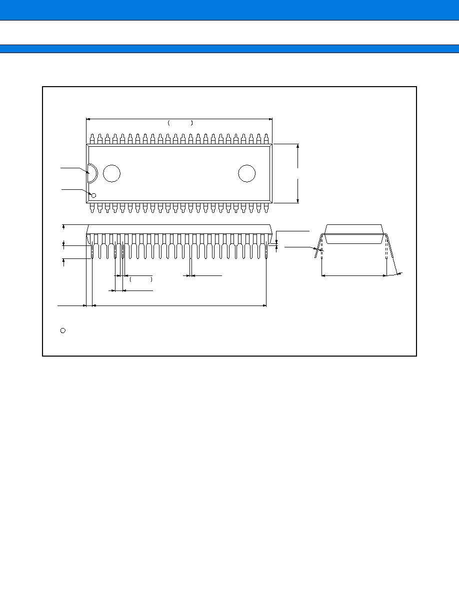
PACKAGE DIMENSIONS
(Continued)
48-pin Plastic SH-DIP
(DIP-48P-M01)
Dimensions in mm (inches)
Note : The values in parentheses are reference values.
C
1994 FUJITSU LIMITED D48002S-3C-3
43.69
+0.20
≠0.30
+.008
≠.012
1.720
13.80±0.25
(.543±.010)
INDEX-1
5.25(.207)
3.00(.118)
0.45±0.10
(.018±.004)
+.020
≠0
.039
≠0
+0.50
1.00
1.778±0.18
(.070±.007)
1.778(.070)
MAX
0.25±0.05
(.010±.002)
15.24(.600)
TYP
15∞MAX
INDEX-2
40.894(1.610)REF
MAX
MIN
0.51(.020)MIN

MB89470 Series
45
(Continued)
48-pin Plastic LQFP
(FPT-48P-M05)
Dimensions in mm (inches)
Note : The values in parentheses are reference values.
C
2002 FUJITSU LIMITED F48013S-c-5-9
24
13
36
25
48
37
INDEX
*7.00 (.276 )SQ
9.00
±0.20(.354±.008)SQ
0.145
±0.055
(.006
±.002)
0.08(.003)
"A"
0∞~8∞
.059
≠.004
+.008
≠0.10
+0.20
1.50
0.50
±0.20
(.020
±.008)
0.60
±0.15
(.024
±.006)
0.10
±0.10
(.004
±.004)
(Stand off)
0.25(.010)
Details of "A" part
1
12
0.08(.003)
M
(.008
±.002)
0.20±0.05
0.50(.020)
LEAD No.
(Mounting height)
+0.40
≠0.10
+.016
≠.004

MB89470 Series
46
(Continued)
48-pin Plastic QFP
(FPT-48P-M13)
Note 1) *: These dimensions do not include resin protrusion.
Note 2) Pins width and pins thickness include plating thickness.
Note 3) Pins width do not include tie bar cutting remainder.
Dimensions in mm (inches)
Note : The values in parentheses are reference values.
C
2003 FUJITSU LIMITED F48023S-c-3-4
(.013±.002)
0.32±0.05
0.80(.031)
M
0.20(.008)
0.10(.004)
(.007±.002)
0.17±0.06
10.00±0.20(.394±.008)SQ
13.10±0.40(.516±.016)SQ
1
12
13
24
37
48
25
36
INDEX
Details of "A" part
0.80±0.20
(.031±.008)
0.88±0.15
(.035±.006)
0.25(.010)
.008
≠.008
+.004
≠0.20
+0.10
0.20
(Stand off)
1.95
+0.40
≠0.20
+.016
≠.008
.077
(Mounting height)
0~8∞
"A"
0.10(.004)
*

MB89470 Series
47
(Continued)
48-pin Ceramic MQFP
(MQP-48C-P01)
Dimensions in mm (inches)
Note : The values in parentheses are reference values.
≠.010
+.018
≠0.25
+0.45
+0.13
≠0.0
+.005
≠0
PIN No.1 INDEX
1.50(.059)TYP
1.00(.040)TYP
8.80(.346)REF
(.0315±.0087)
0.80±0.22
(.016±.003)
0.40±0.08
.043
1.10
0.60(.024)TYP
8.50(.335)MAX
(.006±.002)
0.15±0.05
PAD No.1 INDEX
4.50(.177)TYP
0.30(.012)TYP
TYP
TYP
8.71(.343)
7.14(.281)
(.040±.005)
1.02±0.13
10.92
.430
PIN No.1 INDEX
17.20(.677)TYP
(.591±.010)
15.00±0.25
(.583±.014)
14.82±0.35
1994 FUJITSU LIMITED M48001SC-4-2
C

MB89470 Series
FUJITSU LIMITED
All Rights Reserved.
The contents of this document are subject to change without notice.
Customers are advised to consult with FUJITSU sales
representatives before ordering.
The information, such as descriptions of function and application
circuit examples, in this document are presented solely for the
purpose of reference to show examples of operations and uses of
Fujitsu semiconductor device; Fujitsu does not warrant proper
operation of the device with respect to use based on such
information. When you develop equipment incorporating the
device based on such information, you must assume any
responsibility arising out of such use of the information. Fujitsu
assumes no liability for any damages whatsoever arising out of
the use of the information.
Any information in this document, including descriptions of
function and schematic diagrams, shall not be construed as license
of the use or exercise of any intellectual property right, such as
patent right or copyright, or any other right of Fujitsu or any third
party or does Fujitsu warrant non-infringement of any third-party's
intellectual property right or other right by using such information.
Fujitsu assumes no liability for any infringement of the intellectual
property rights or other rights of third parties which would result
from the use of information contained herein.
The products described in this document are designed, developed
and manufactured as contemplated for general use, including
without limitation, ordinary industrial use, general office use,
personal use, and household use, but are not designed, developed
and manufactured as contemplated (1) for use accompanying fatal
risks or dangers that, unless extremely high safety is secured, could
have a serious effect to the public, and could lead directly to death,
personal injury, severe physical damage or other loss (i.e., nuclear
reaction control in nuclear facility, aircraft flight control, air traffic
control, mass transport control, medical life support system, missile
launch control in weapon system), or (2) for use requiring
extremely high reliability (i.e., submersible repeater and artificial
satellite).
Please note that Fujitsu will not be liable against you and/or any
third party for any claims or damages arising in connection with
above-mentioned uses of the products.
Any semiconductor devices have an inherent chance of failure. You
must protect against injury, damage or loss from such failures by
incorporating safety design measures into your facility and
equipment such as redundancy, fire protection, and prevention of
over-current levels and other abnormal operating conditions.
If any products described in this document represent goods or
technologies subject to certain restrictions on export under the
Foreign Exchange and Foreign Trade Law of Japan, the prior
authorization by Japanese government will be required for export
of those products from Japan.
F0303
©
FUJITSU LIMITED Printed in Japan