
Pr
eliminar
y
MBF110
Solid-State Fingerprint Sensor
Applications
∑ Database and network access
∑ Portable fingerprint acquisition
∑ Access control (home, auto, office, etc.)
∑ ATM
∑ Smart cards
∑ Cellular phone security access
Overview
The Fujitsu MBF110 Solid-State Fingerprint Sensor is a direct
contact, fingerprint acquisition device. It is a high performance,
low power, low cost, capacitive sensor with an integrated two-
dimensional array of metal electrodes in the sensing array. Each
metal electrode acts as one plate of a capacitor and the contacting
finger acts as the second plate. A passivation layer on the device
surface forms the dielectric between these two plates. Ridges and
valleys on the finger yield varying capacitor values across the array,
which is read to form an image of the fingerprint.
The MBF110 is manufactured in standard CMOS technology and
is available in an 80-pin, VSPA 80/1 and LQFP 80/1. The 300
◊
300 sensor array has a 50
µ
m pitch and yields a 500-dpi image. The
sensor surface is protected by a patented, ultra-hard, abrasion and
chemical resistant coating.
80-pin TSOP (LQFP)
80-pin SOP (VSPA)
Packages
A block diagram of the MBF110 is shown in Figure 1. The
MBF110 has an integrated 8-bit flash analog-to-digital converter
to digitize the output of the sensor array. The fingerprint image is
transmitted on an 8-bit bi-directional bus interface compatible
with most microprocessors.
For SETCUR resistor differences between the MBF110 see the Pin
Information table.
Features
∑ Non-optical solid-state device
∑ 300
◊
300 sensor array, 50
µ
m pitch
∑ 1.5 cm
◊
1.5 cm sensor area
∑ 500-dpi resolution
∑ Operation from 3V to 5.5V
∑ Ultra-hard protective coating
∑ Integrated 8-bit flash analog-to-digital converter
∑ 8-bit microprocessor interface
∑ Standard CMOS technology
∑ Low power, less than 200 mW


Pr
eliminar
y
MBF110
Fujitsu Microelectronics, Inc.
-1
Table of Contents
Chip Operation .....................................................................................................................................................................1
Special Features ....................................................................................................................................................................2
MBF110 Pin Information for SOP 80/1 .................................................................................................................................. 2
MBF110 Connection Diagram ................................................................................................................................................3
Function Table ......................................................................................................................................................................4
Register Map ........................................................................................................................................................................4
Address Register Descriptions .................................................................................................................................................4
RAL (A3-A0 Address 0000) Write Only .............................................................................................................................4
Low Order Row Address Register ................................................................................................................................4
RAH (A3-A0 Address 0001) Write Only ............................................................................................................................5
High Order Row Address Register ...............................................................................................................................5
CAL (A3-A0 Address 0010) Read/Write.............................................................................................................................5
Low Order Column Address Register ...........................................................................................................................5
CAH (A3-A0 Address 0011) Write Only .............................................................................................................................6
High Order Column Address Register ..........................................................................................................................6
DTR (A3-A0 Address 0100) Write Only .............................................................................................................................6
Discharge Time Register ............................................................................................................................................6
DCR (A3-A0 Address 0101) Write Only .............................................................................................................................7
Discharge Current Register........................................................................................................................................7
RSR (A3-A0 Address 0110) Write Only ..............................................................................................................................7
Reserved..................................................................................................................................................................7
Row Capture and A/D Conversion Timing .................................................................................................................................8
A/D Converter ......................................................................................................................................................................8
Specifications ........................................................................................................................................................................8
Absolute Maximum Ratings ....................................................................................................................................................8
Operating Range ...................................................................................................................................................................8
DC Electrical Characteristics ..................................................................................................................................................8
Power Supply Characteristics,
(V
DD
= 5.5V, f
OSC
= 40 MHz Standard Temperature Range)..................................................................................................9
Power Supply Characteristics,
(V
DD
= 3.6V, Commercial Temperature Range, f
OSC
= 20 MHz ) ............................................................................................9
Read Cycle Timing at V
DD
= 3.0V, Standard Temperature Range................................................................................................10
Write Cycle Timing at V
DD
= 3.0V, Standard Temperature Range ...............................................................................................11
Power Up and Initialization ..................................................................................................................................................12
Image Capture ....................................................................................................................................................................13
Fujitsu Microelectronics, Inc.

Pr
eliminar
y
Solid-State Fingerprint Sensor
0
Fujitsu Microelectronics, Inc.
MBF110 ≠ PFW1, SOP (VSPA) ≠ 80 pin Package .................................................................................................................. 14
MBF110 ≠ PFW, TSOP (LQFP) ≠ 80 pin Package .................................................................................................................. 15
MBF110 Solder Pad Layout................................................................................................................................................. 16
Manufacturing Considerations.............................................................................................................................................. 17
Array Pixel Specifications .................................................................................................................................................... 17
MBF110 Ordering Information ............................................................................................................................................ 18
Fujitsu Microelectronics, Inc.
Pr
eliminar
y
MBF110
Fujitsu Microelectronics, Inc.
1
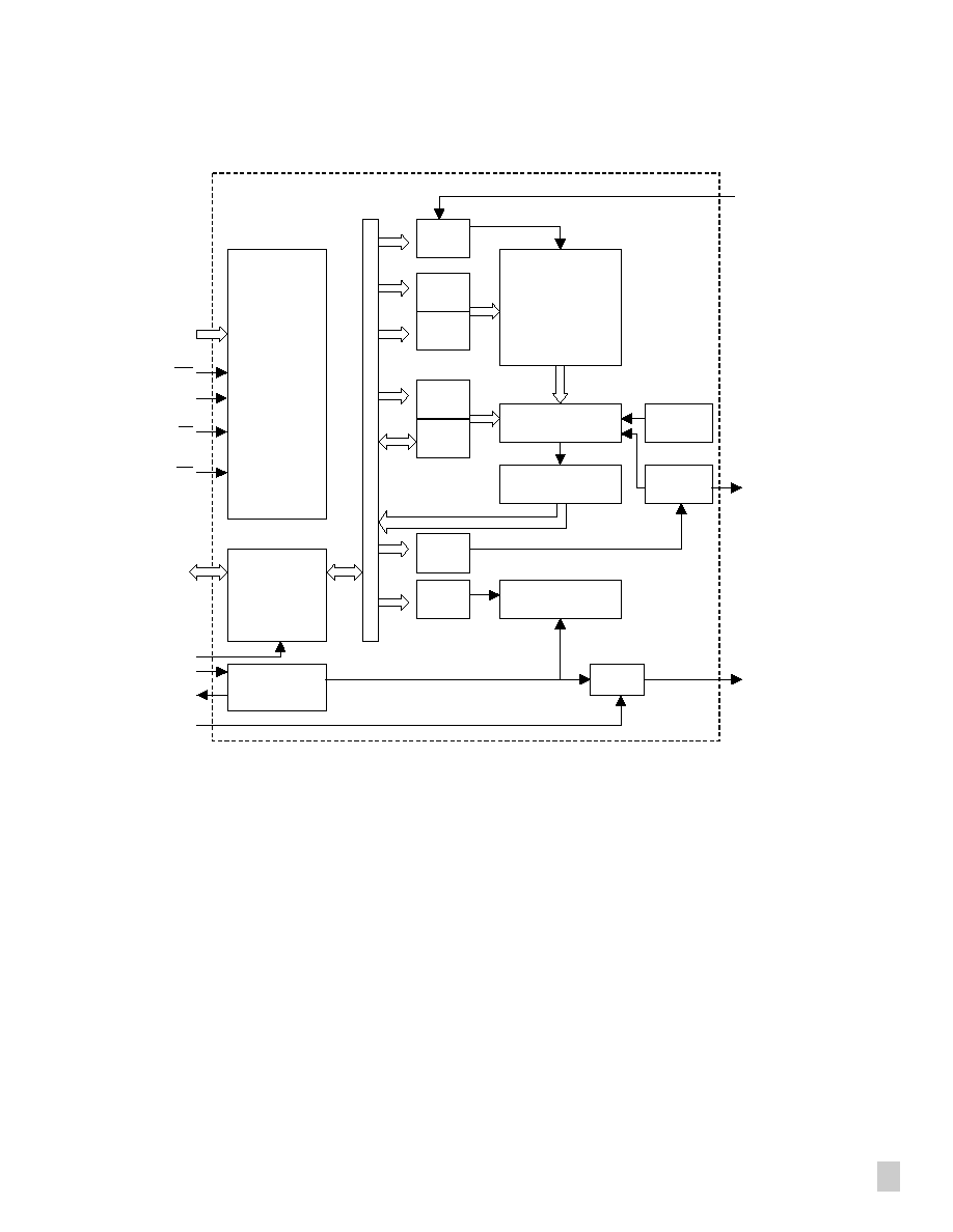
Figure 1.
MBF110 Block Diagram
OSCILLATOR
DATA
BUS
BUFFER
DCR
RAH
RAL
CAH
CAL
RSR
DTR
300 x 300
Sensor Arrays
CONTROL LOGIC
MUX
8 Bit A/D
Temperature
Sensor
Resistance
Sensor
CLK OUT
SELECT
LOGIC
A[3:0]
CE1
CE2
RD
WR
D[7:0]
TEST
XTAL1
XTAL2
ENCLK
RSENSE
CLK
SETCUR
Chip Operation
The sensor array is composed of 300 rows and 300 columns of sensor
plates. Associated with each column are two sample-and-hold
circuits. A fingerprint image is sensed or captured one row at a time.
This "row capture" occurs in two phases. In the first phase, the
sensor plates of the selected row are pre-charged to the V
DD
voltage.
During this pre-charge period, an internal signal enables the first set
of sample-and-hold circuits to store the pre-charged plate voltages of
the row.
In the second phase, the row of sensor plates is discharged with a
current source. The rate at which a cell is discharged is proportional
to the "discharge current." After a period of time (referred to as the
"discharge time"), an internal signal enables the second set of
sample-and-hold circuits to store the final plate voltages. The
difference between the pre-charged and discharged plate voltages is a
measure of the capacitance of a sensor cell. After the row capture, the
cells within the row are ready to be digitized.
The sensitivity of the chip is adjusted by changing the discharge
current and discharge time. The nominal value of the current source
is controlled by an external resistor connected between the SETCUR
pin and ground. The current source is controlled from the Discharge
Current Register (DCR). The discharge time is controlled by the
Discharge Time Register (DTR).
The sensor array is a row-oriented device. Images are read out one
row at a time. The High-Order Row Address Register (RAH) and the
Low-Order Row Address Register (RAL) must be programmed to
select a row to be captured. Writing to RAL initiates a row capture.
The capture time is a function of the external clock and the DTR.
After the discharge cycle, the outputs of the row elements will be
stored in analog sample and hold circuits.

Pr
eliminar
y
Solid-State Fingerprint Sensor
2
Fujitsu Microelectronics, Inc.
After the row capture is completed, the High-Order Column Address
Register (CAH) and Low-Order Column Address Register (CAL)
must be programmed to select an element within the captured row to
be digitized. Writing to CAL causes the analog-to-digital (A/D)
converter to digitize the difference between the outputs of the two
sample-and-holds of the selected column cell. The output of the A/D
converter is accessed by reading the CAL register.
Rows can be accessed in any order; however, the selected row must be
captured before the column cells are read. The column cells within a
row can be accessed in any order.
Special Features
There are two programmable open-drain outputs that can be used
for driving LEDs.
The CLKOUT pin can be enabled to output a square-wave clock of
the same frequency as the oscillator clock. CLKOUT can be used to
drive external circuitry. When ENCLK is high, the clock signal is
present at the CLKOUT pin. When ENCLK is low or unconnected,
the CLKOUT output is held low.
MBF110 Pin Information for SOP (VSPA) 80/1
Pin
Number
Pin
Name
Type
Description
Notes
34
A3
Input
Address Inputs
Address signals connected to these pins select a register to read from or write to dur-
ing data transfer.
35
A2
36
A1
37
A0
38
CE1
Chip Enable, Active Low
When CE1 is low and CE2 is high, the chip is selected.
39
CE2
Chip Enable, Active High
When CE1 is low and CE2 is high, the chip is selected.
40
RD
Read Enable, Active Low
This pin must be low while WR is high and the chip selected in order to read a register
on the chip.
17
WR
Write Enable, Active Low
This pin must be low while the chip is selected to write to a register on the chip.
18
D7
Bi-directional
Data Bus
Inputs when WR is low and chip is selected. Outputs when RD is low, WR is high, and
chip is selected.
19
D6
21
D5
22
D4
24
D3
25
D2
26
D1
27
D0
32
CLKOUT
Output
Clock Output
This pin outputs the oscillator clock frequency when ENCLK is high.
31
ENCLK
Input
Enable Clock Output
A high on this pin enables the CLKOUT pin. A low on this pin holds CLKOUT low.
ENCLK has an internal pull-down resistor.
15
LED1
Open-drain
Output
LED driver
This pin can be used to drive an LED.
14
LED2
Open-drain
Output
3
SETCUR
Input
Set Discharge Current
Place an external resistor R1 (200K ≠ 680K ohms) between this pin and ground.
Typical: FPS110, R1 = 680K; FPS110B, R1 = 200K; FPS110E, R1 = 200K
2
N/A
Reserved pin
Must be left disconnected.
13
TEST
20, 33
V
DD
Power
Digital Power Supply
1
V
DDA
Analog Power Supply
Pr
eliminar
y
MBF110
Fujitsu Microelectronics, Inc.
3
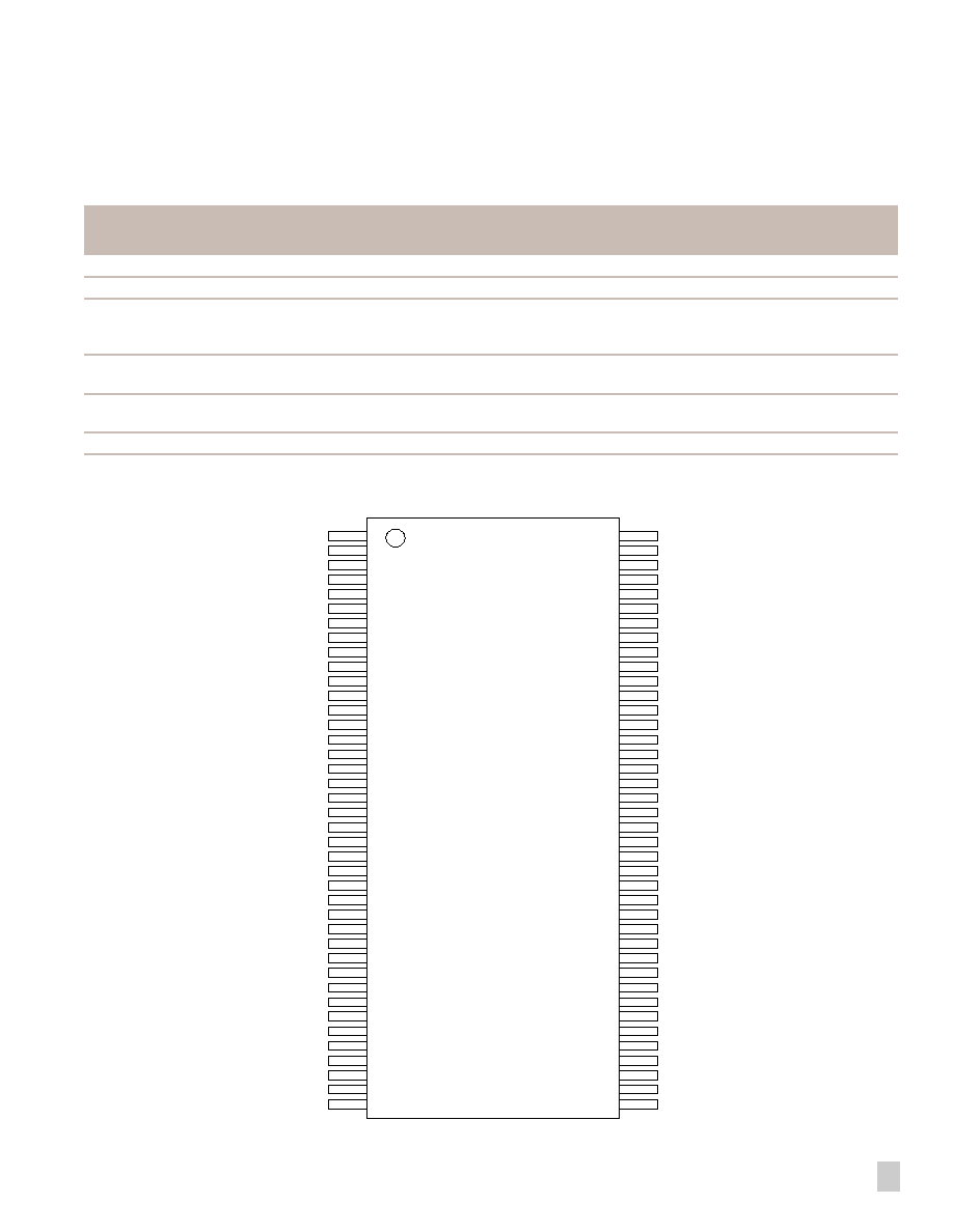
MBF110 Connection Diagram
16, 23, 28
V
SS
Ground
Digital ground
4, 5
V
SSA
(Center)
Analog ground
29
XTAL1
Input
Input to the On-Chip
Oscillator
To use the internal oscillator connect a crystal circuit to this pin. If an external oscilla-
tor is used, its output is connected to this pin. XTAL1 is the clock source for internal
timing.
30
XTAL2
Output
Output of the On-Chip
Oscillator
To use the internal oscillator connect a crystal circuit to this pin. If an external oscilla-
tor is used, leave XTAL2 unconnected.
41-80
GNDSHLD
Shield Ground
Connected to Package Top
Plate
These pins should connect to chassis ground.
2, 6-12
N/A
N/A
Not connected.
MBF110 Pin Information for SOP (VSPA) 80/1 (Continued)
Pin
Number
Pin
Name
Type
Description
Notes
VDDA
Reserved
SETCUR
VSSA
VSSA
Unconnected
Unconnected
Unconnected
Unconnected
Unconnected
Unconnected
Unconnected
TEST
LED2
LED1
VSS
VSS
VSS
WR-
D7
D6
VDD
VDD
D5
D4
D3
D2
D1
D0
XTAL1
XTAL2
ENCLK
CLKOUT
A3
A2
A1
A0
CE1-
CE2
RD-
GNDSHLD
GNDSHLD
GNDSHLD
GNDSHLD
GNDSHLD
GNDSHLD
GNDSHLD
GNDSHLD
GNDSHLD
GNDSHLD
GNDSHLD
GNDSHLD
GNDSHLD
GNDSHLD
GNDSHLD
GNDSHLD
GNDSHLD
GNDSHLD
GNDSHLD
GNDSHLD
GNDSHLD
GNDSHLD
GNDSHLD
GNDSHLD
GNDSHLD
GNDSHLD
GNDSHLD
GNDSHLD
GNDSHLD
GNDSHLD
GNDSHLD
GNDSHLD
GNDSHLD
GNDSHLD
GNDSHLD
GNDSHLD
GNDSHLD
GNDSHLD
GNDSHLD
GNDSHLD
1
2
3
4
5
6
7
8
9
10
11
12
13
14
15
16
17
18
19
20
21
22
23
24
25
26
27
28
29
30
31
32
33
34
35
36
37
38
39
40
80
79
78
77
76
75
74
73
72
71
70
69
68
67
66
65
64
63
62
61
60
59
58
57
56
55
54
53
52
51
50
49
48
47
46
45
44
43
42
41

Pr
eliminar
y
Solid-State Fingerprint Sensor
4
Fujitsu Microelectronics, Inc.
Function Table
Register Map
CE1
CE2
RD
WR
Mode
Data Lines
H
X
X
X
De-selected
High-Z
X
L
X
X
De-selected
High-Z
L
H
H
H
Standby
High-Z
L
H
L
H
Read
Data Out
L
H
H
L
Write
Data In
A3
A2
A1
A0
Access
Register
Description
0
0
0
0
Write
RAL
Low Order Row Address Register
0
0
0
1
Write
RAH
High Order Row Address Register
0
0
1
0
Read/Write
CAL
Low Order Column Address Register
0
0
1
1
Write
CAH
High Order Column Address Register
0
1
0
0
Write
DTR
Discharge Time Register
0
1
0
1
Write
DCR
Discharge Current Register
0
1
1
0
Write
RSR
Reserved
MSB
LSB
BIT7
BIT6
BIT5
BIT4
BIT3
BIT2
BIT1
BIT0
RA7
RA6
RA5
RA4
RA3
RA2
RA1
RA0
Bit Number
Bit Name
Function
[7:0]
RA[7:0]
Low eight bits of Row Address Register.
Address Register Descriptions
Refer to
Row Capture and A/D Conversion Timing
on page 9 to
calculate row capture and A/D conversion times.
RAL (A3-A0 Address 0000) Write Only
Low Order Row Address Register
This register and bit 0 of RAH form the 9-bit Row Address Register
that selects the row to be captured. The 9-bit Row Address Register
selects a row address from 0 through 299. Writing the RAL starts a
row capture. Only RAL has to be written if RAH doesn't change,
otherwise RAH has to be written before RAL.

Pr
eliminar
y
MBF110
Fujitsu Microelectronics, Inc.
5
RAH (A3-A0 Address 0001) Write Only
High Order Row Address Register
Bit 0 of this register and RAL form the 9-bit Row Address Register
that selects the row to be converted. The L1 and L2 bits control two
open-drain outputs that can be used to drive LEDs.
MSB
LSB
BIT7
BIT6
BIT5
BIT4
BIT3
BIT2
BIT1
BIT0
L1
L2
≠
≠
≠
≠
≠
RA8
Bit Number
Bit Name
Function
7
L1
L1=0, LED1 output low
L1=1, LED1 output high-Z
6
L2
L2=0, LED 2 output low
L2=1, LED 2 output high-Z
[5:1]
≠
Reserved, write 0 to these bits.
0
RA8
MSB of Row Address
CAL (A3-A0 Address 0010) Read/Write
Low Order Column Address Register
CAL is a read/write register. Writing to this address writes to the
low-order 8 bits of the 9-bit Column Address Register. The 9-bit
Column Address Register selects a column from 0 through 299.
Writing to CAL causes the analog-to-digital (A/D) converter to
begin digitizing its input. The input of the A/D converter is selected
by bits 7 and 6 of the CAH register. The user should wait until the
row capture is completed before writing to the CAL.
Reading from this address returns the output of the A/D converter.
After writing to CAL, the user should wait until A/D conversion
completes before reading the A/D converter.
MSB
LSB
BIT7
BIT6
BIT5
BIT4
BIT3
BIT2
BIT1
BIT0
CA7
CA6
CA5
CA4
CA3
CA2
CA1
CA0
Bit Number
Bit Name
Function
[7:0]
CA[7:0]
(WRITE) Low eight bits of Column Address Register.
(READ) Output of A/D converter.

Pr
eliminar
y
Solid-State Fingerprint Sensor
6
Fujitsu Microelectronics, Inc.
CAH (A3-A0 Address 0011) Write Only
High Order Column Address Register
Bit 0 of this register and CAL form the 9-bit Column Address
Register that selects a cell from the current row for digitizing.
The user should wait until the row capture is completed before
writing to CAH.
MSB
LSB
BIT7
BIT6
BIT5
BIT4
BIT3
BIT2
BIT1
BIT0
R
T
≠
≠
≠
≠
≠
CA8
Bit Number
Bit Name
Function
[7:1]
≠
Reserved, write 0 to these bits.
0
CA8
MSB of Column Address Register
DTR (A3-A0 Address 0100) Write Only
Discharge Time Register
MSB
LSB
BIT7
BIT6
BIT5
BIT4
BIT3
BIT2
BIT1
BIT0
PD
T6
T5
T4
T3
T2
T1
T0
Bit Number
Bit Name
Function
7
PD
Power down chip.
PD=0, Chip in Normal Mode
PD=1, Chip in Low Power Mode
[6:0]
T[6:0]
Selects the count to be loaded into the Discharge Timer. Discharge time is selected in increments of the
oscillator period. Discharge Time is defined as the period between the sampling and holding of the pre-charged
sensor cell to the sampling and holding of the discharging sensor cell. The Discharge Time can be calculated
from the following equation:
Discharge Time = T[6:0] * t
OSC
Pr
eliminar
y
MBF110
Fujitsu Microelectronics, Inc.
7
DCR (A3-A0 Address 0101) Write Only
Discharge Current Register
MSB
LSB
RSR (A3-A0 Address 0110) Write Only
Reserved
The user must initialize this resistor to zero.
MSB
LSB
BIT7
BIT6
BIT5
BIT4
BIT3
BIT2
BIT1
BIT0
F2
F1
TRST
DC4
DC3
DC2
DC1
DC0
Bit Number
Bit Name
Function
[7:6]
F2, F1
These two bits tell the chip the frequency of the external oscillator or crystal that is connected to the chip.
F2
F1
XTAL Input
0
0
10-15 MHz
0
1
15-20 MHz
1
0
20-30 MHz
1
1
30-40 MHz
5
TRST
Timer Reset. Set this bit to halt and reset the Discharge Timer. Resetting the Discharge Timer is necessary to put
the Discharge Timer in a known state after power-up or after returning to Normal mode from Low-power mode
(See bit 7 of DTR).
TRST=0,Normal Timer Operation
TRST=1,Halt and Clear Discharge Timer (doesn't clear DTR)
[4:0]
DC[4:0]
Selects the Discharge Current source value.
BIT7
BIT6
BIT5
BIT4
BIT3
BIT2
BIT1
BIT0
≠
≠
≠
≠
≠
≠
≠
≠
Bit Number
Bit Name
Function
[7:0]
≠
Reserved. Write 0 to these bits.

Pr
eliminar
y
Solid-State Fingerprint Sensor
8
Fujitsu Microelectronics, Inc.
Row Capture and A/D Conversion Timing
NOTE: n is selected by bits T[6:0] of DTR.
F2
F1
XTAL Input Range
Row Capture Time in OSC Clock Periods
A/D Conversion Time in OSC Clock Periods
0
0
10-15 MHz
18+n
13
0
1
15-20 MHz
24+n
15
1
0
20-30 MHz
36+n
23
1
1
30-40 MHz
48+n
30
A/D Converter
The integrated 8-bit flash A/D converter is a buffered device. Each
write to CAL causes: 1) the result of the previous conversion to be
latched and made readable at CAL, and 2) the A/D converter to start
digitizing its current input. Consequently, it takes 301 writes to
CAL in order to digitize the 300 cells of a row.
Specifications*
*All specifications in this document are preliminary and subject to
change.
Absolute Maximum Ratings
∑ Storage Temperature:
-65∞ to +150∞ C
∑ DC Voltage Applied to any Pins: -0.5 V to +7.0 V
Operating Range
DC Electrical Characteristics
Symbol
Parameter
Min
Max
Unit
V
DD
Digital Supply Voltage
+3.0
+5.5
V
V
DDA
Analog Supply Voltage
+3.0
+5.5
V
Standard Temperature Range
0
60
∞
C
f
OSC
Oscillator Frequency V
DD
= 5.0V
V
DD
= 3.0V
10
40
MHz
10
20
MHz
Symbol
Parameter
Test Conditions
Min
Max
Unit
V
OH
Output High Voltage
V
DD
= 4.5V, I
OH
= -4 mA
2.4
≠
V
V
OL
Output Low Voltage
V
DD
= 4.5V, I
OL
= 8 mA
≠
0.4
V
V
OH
Output High Voltage
V
DD
= 3.0V, I
OH
= -2 mA
2.4
-
V
V
OL
Output Low Voltage
V
DD
= 3.0V, I
OL
= 4 mA
≠
0.4
V
V
IH
Input High Voltage
2.0
V
DD
V
V
IL
Input Low Voltage
V
DD
= 4.5V
-0.5
0.8
V
V
IL
Input Low Voltage
V
DD
= 3.00
-0.5
0.6
V
I
LI
Input Leakage Current
GND
V
in
5.5V
-5.0
5.0
µA
I
LO
Output Leakage Current
GND
V
out
5.5V
-5.0
5.0
µA

Pr
eliminar
y
MBF110
Fujitsu Microelectronics, Inc.
9
Power Supply Characteristics
(V
DD
= 5.5V, f
OSC
=40 MHz Standard Temperature Range)
Note: Analog supply currents are independent of f
OSC
Note: XTAL2 & CLKOUT driving C
LOAD
= 50pF
Power Supply Characteristics
V
DD
= 3.6V, Commercial Temperature Range, f
OSC
= 20 MHz
Note: Analog supply currents are independent of f
OSC
Note: XTAL2 & CLKOUT driving C
LOAD
= 50 Pf
Symbol
Parameter
Test Conditions
Typ
Max
Unit
LP
STD
LP
STD
I
DD1
Digital Supply Current
Power down with CLKOUT disabled, (DTR bit 7 = 1, ENCLK = 0)
<1
100
50
100
µA
I
DD2
Power down with CLKOUT enabled.
( DTR bit 7 = 1, ENCLK = 1)
17
20
20
25
mA
I
DD3
Idle with CLKOUT disabled.
(DTR bit 7 = 0, ENCLK = 0)
8
10
12
15
mA
I
DD4
Idle with CLKOUT enabled.
( DTR bit 7 = 0, ENCLK = 1)
17
20
20
25
mA
I
DD5
Active A/D conversion with CLKOUT disabled.
(DTR bit 7 = 0, ENCLK = 0)
15
20
25
30
mA
I
DD6
Active A/D conversion with CLKOUT enabled.
(DTR bit 7 = 0, ENCLK = 1)
25
30
30
35
mA
I
DDA
Analog Supply Current
Power down with CLK disabled or enabled.
(DTR bit 7 = 1)
<10
<100
50
1000
µA
IDLE with CLKOUT disabled or enabled,
(DTR bit 7 = 0)
15
20
22
25
mA
Active A/D conversion with CLKOUT disabled or enabled. (DTR bit 7 = 0)
18
22
26
30
mA
Symbol
Parameter
Test Conditions
Typ
Max
Unit
LP
STD
LP
STD
I
DD1
Digital Supply Current
Power down with CLKOUT disabled.
(V
DD
= max, f
OSC
= max, DTR bit 7 = 1, ENCLK = 0)
<1
<10
50
100
µA
I
DD2
Power down with CLKOUT enabled.
(V
DD
= max, f
OSC
= max, DTR bit 7 = 1, ENCLK = 1)
6
10
10
15
mA
I
DD3
Idle with CLKOUT disabled.
(V
DD
= max, f
OSC
= max, DTR bit 7 = 0, ENCLK = 0)
3
5
6
10
mA
I
DD4
Idle with CLKOUT enabled.
(V
DD
= max, f
OSC
= max, DTR bit 7 = 0, ENCLK = 1)
6
10
10
15
mA
I
DD5
Active A/D conversion with CLKOUT disabled.
(V
DD
= max, f
OSC
= max, DTR bit 7 = 0, ENCLK = 0)
6
10
10
15
mA
I
DD6
Active A/D conversion with CLKOUT enabled.
(V
DD
= max, f
OSC
= max, DTR bit 7 = 0, ENCLK = 1)
9
13
13
18
mA
I
DDA
Analog Supply Current
Power down with CLK disabled or enabled.
(V
DDA
= max, DTR bit 7 = 1)
<2
<10
50
1000
µA
IDLE with CLKOUT disabled or enabled, (DTR bit 7 = 0)
10
15
15
20
mA
Active A/D conversion with CLKOUT disable or enable. (DTR bit 7 = 0)
12
15
18
25
mA

Pr
eliminar
y
Solid-State Fingerprint Sensor
10
Fujitsu Microelectronics, Inc.
Read Cycle Timing at V
DD
= 3.0V, Standard Temperature Range
Figure 2.
Read Cycle Timing
Parameter
Description
Min
Max
Unit
t
AAC
Address valid to data valid.
≠
70
ns
t
RC
Read Cycle Time
70
≠
ns
t
ACE1
CE1 low to data valid
≠
70
ns
t
ACE2
CE2 high to data valid
≠
70
ns
t
DOE
RD low to data valid
≠
35
ns
t
LZOE
RD low to low Z
5
≠
ns
t
HZOE
RD high to high Z
≠
30
ns
t
LZCE
CE1 low and CE2 high to low Z
5
≠
ns
t
HZCE
CE1 high to high Z or CE2 low to high Z
≠
30
ns
t
LZWE
WR high to low Z
5
≠
ns
t
HZWE
WR low to high Z
≠
30
ns
A[3:0]
CE1
CE2
RD
WR
DATA OUT
t
AAC
t
RC
t
ACE1
t
ACE2
t
DOE
t
HZOE
t
HZWE
t
LZWE
t
LZOE
t
LZCE
t
HZCE
Data Valid
High Z

Pr
eliminar
y
MBF110
Fujitsu Microelectronics, Inc.
11
Write Cycle Timing at V
DD
= 3.0V, Standard Temperature Range
Figure 3.
Write Cycle Timing
Parameter
Description
Min
Max
Unit
t
WC
Write Cycle
70
≠
ns
t
SCE1
CE1 low to write end
60
≠
ns
t
SCE2
CE2 high to write end
60
≠
ns
t
AW
Address setup to write end
55
≠
ns
t
HA
Address hold from write end
5
≠
ns
t
SA
Address set-up to write start
5
≠
ns
t
PWE
WR Pulse Width
40
≠
ns
t
SD
Data setup to write end
35
≠
ns
t
HD
Data hold from write end
5
≠
ns
CE1
CE2
RD
WR
DATA IN
t
SA
t
HA
t
AW
t
SCE1
t
SCE2
t
PWE
t
SD
t
HD
A[3:0]

Pr
eliminar
y
Solid-State Fingerprint Sensor
12
Fujitsu Microelectronics, Inc.
Power Up and Initialization
Write DTR with PD bit set
Power-Up
Set DTR[7] (PD) to power down device.
Wait 1
µs
Write DTR with
PD bit clear
Write DCR with TRST set
Write DCR with
TRST clear
Wait for chip to power down.
Clear TRST for normal dicharge timer operation.
DCR[4:0] initialized to known values.
Wait for chip to return from power-down.
Clear DTR[7] (PD) to return from power-down.
DTR[6:0] initialized to known values.
Set DCR[5] (TRST) to halt and reset the discharge
timer.
Initialize RSR to zero.
Clear RSR
Initialization Done
Wait 10
µs
Pr
eliminar
y
MBF110
Fujitsu Microelectronics, Inc.
13
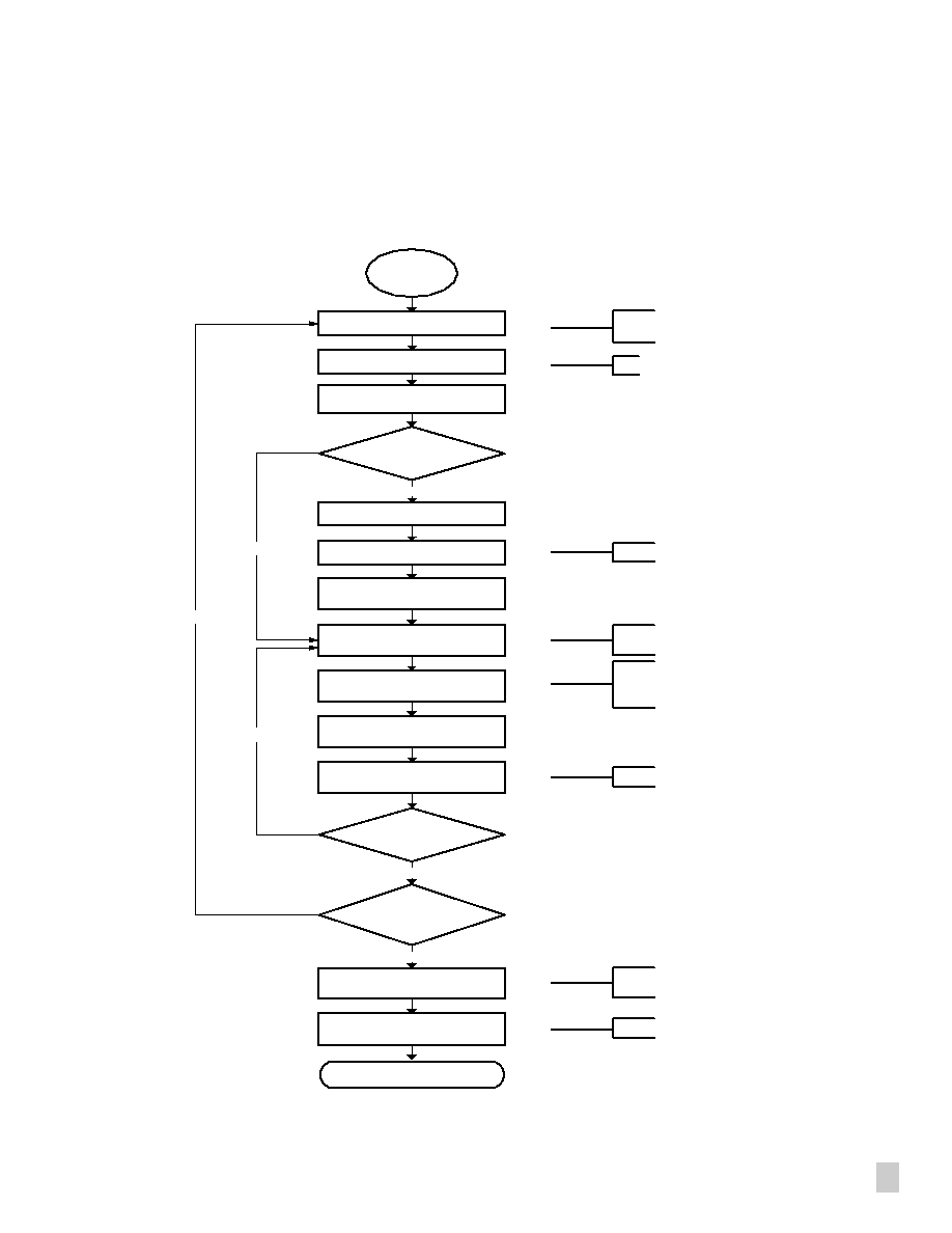
Image Capture
Write RAH if needed
Begin
Image
Capture
Initiates row capture.
Write CAH
Write CAL
Wait until row capture
completes
Write RAL
First A/D conversion
of image
Wait until A/D conversion
completes
Write CAL
Write CAH if needed
Wait until A/D conversion
completes
Read CAL
Write CAL
Read CAL
Converted
all cells in current
row?
Converted
last cell of image
Image Captured
Yes
Yes
Yes
No
No
Initiates first A/D conversion.
Read output buffer.
Initiates A/D conversion and
transfers previous result to output
buffer.
Needed to transfer result of last
A/D conversion to output buffer.
Read value of last cell.
Needed if new value to be written
differs from current CAH contents
Needed if new value to be written
differs from current RAH contents
No
Pr
eliminar
y
Solid-State Fingerprint Sensor
14
Fujitsu Microelectronics, Inc.
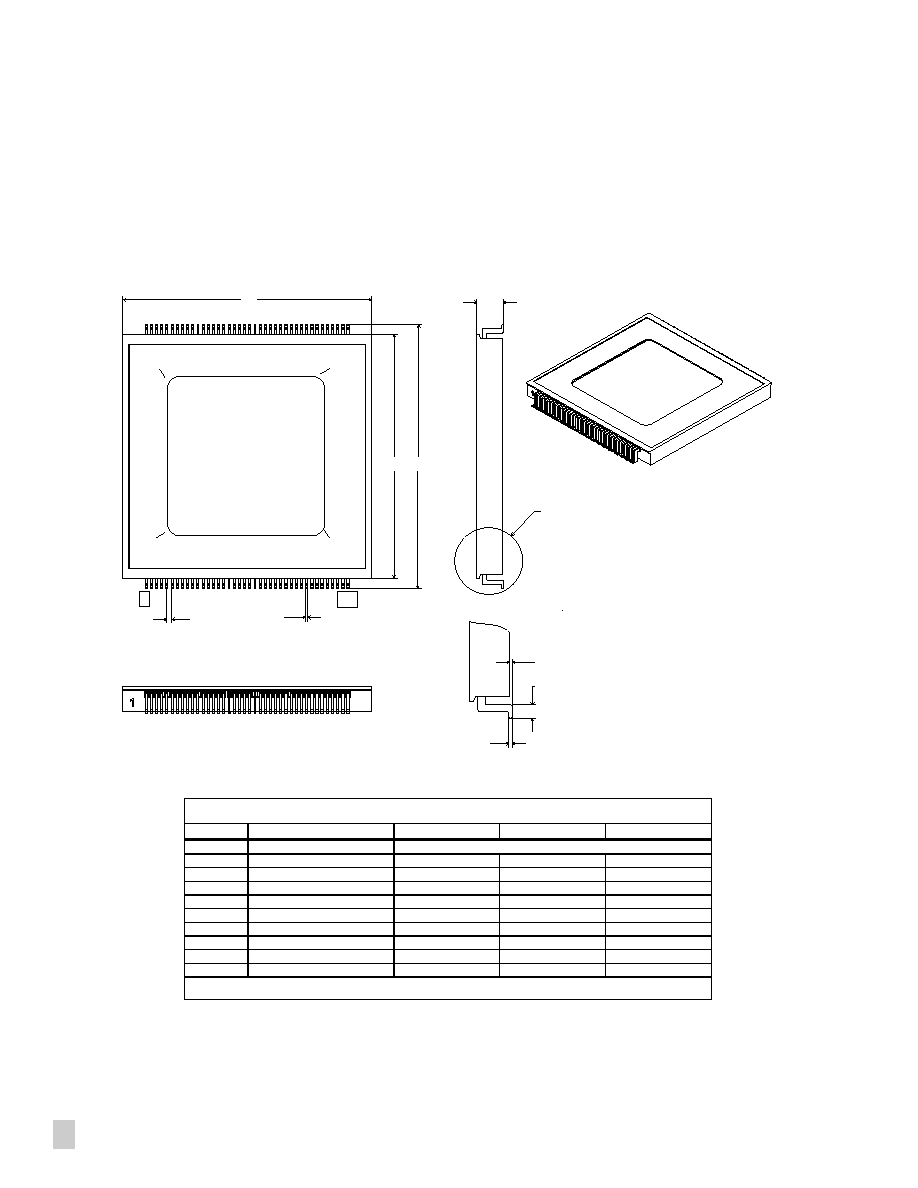
MBF110 ≠ PFW1
SOP (VSPA) ≠ 80 pin Package
MBF110-PFW1: SOP 80pin Assembly Diagram
MBF110 Dimensions
Symbol Description
Min
Nom
Max
N Pin
Count
80
A Overall
Height
A1 Stand
Off
B Pin
Width
C Pin
Thickness
D
Tip to tip Dimension
.941 (23.9)
.941 (23.9)
.0187 (.47)
1.016 (25.8)
.008 (.20)
.008 (.20)
.945 (24.0)
.945 (24.0)
.032 (.81)
.0207 (.53)
.949 (24.1)
.949 (24.1)
1.032 (26.2)
.0197 (.50)
1.025 (26.0)
.006 (.15)
.102 (2.60)
D1 Package
Body
Package Body
E1
F
Pin Pitch
L1 Foot
length
Note: Dimensions are in inches (mm)
E1
D1
A1
L1
C
DETAIL Z
Row 299
Column 0
Detail Z
Row 0
Column 0
Row 299
Column 299
Row 0
Column 299
B
F
D
1
40
A
Pr
eliminar
y
MBF110
Fujitsu Microelectronics, Inc.
15
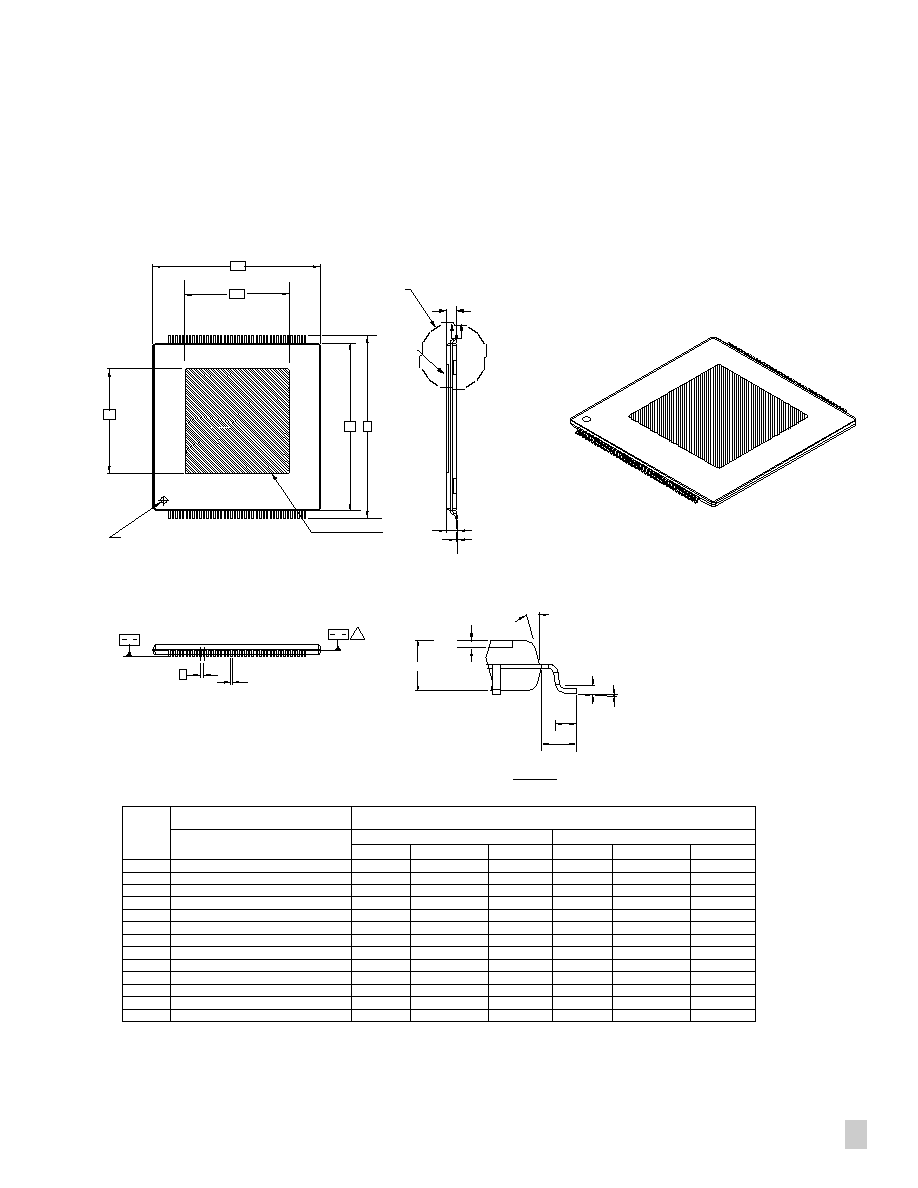
MBF110 ≠ PFW
TSOP (LQFP)≠ 80 pin Package
MBF110-PFW: TSOP 80pin Assembly Diagram
Symbol Description
MBF110PFW
DIMENSIONS
Min.
Nom.
Max.
Min.
Nom.
Millimeters
Inches
Max.
A
A1
A2
b
D1
D3
ddd
E
E1
E3
e
L
L1
1.45
0.10
1.35
0.16
14.95
0.25
14.95
0.50
1.55
0.15
1.40
0.25
24.00 BSC.
15.00
0.30
26.00 BSC.
24.00 BSC.
15.00
0.50 TYP.
0.60
1.00 REF.
1.70
0.25
1.45
0.30
15.05
0.35
15.05
0.70
0.57
.004
.053
.006
.588
.010
.588
.020
0.61
.006
.055
.010
.945 BSC.
.590
.012
1.024 BSC.
.945 BSC.
.590
.0197 TYP.
.024
.039 REF.
0.67
.010
.057
.012
.592
.014
.592
.028
Overall Height
Stand Off
Package Thickness
Lead Width
Package Body
Sensor Array Width
Sensor Array Depth
Tip to Tip Dimension
Package Body
Sensor Array Height
Lead Pitch
Lead Length
Foot Length
D1
SEE DETAIL "B"
A2
1
40
ddd
A A
D3
E3
C
H
2
1.40 ±0.05
ddd
15∞ TYP
D.25 REF. PLANE
DETAIL "B"
3∞-5∞
L
L1
e
b
E1
1
A1
SENSOR ARRAY
1.00 DIA.
PIN NO. 1 IDENTIFIER
A
SEATING
PLANE
SEATING
PLANE
E

Pr
eliminar
y
Solid-State Fingerprint Sensor
16
Fujitsu Microelectronics, Inc.
MBF110 Solder Pad Layout
Symbol Description
Dimension
N Pin
Count
Pad Length
Pad Width
80
A
Tip to Tip Dimension
1.074 (27.30)
P Pitch
.0197 (.50)
L
.065 (1.65)
W
.012 (.30)
Note: Dimensions are in inches (mm)
P
L
A
1
40
W
See Detail Z
Full Radius
Typical

Pr
eliminar
y
MBF110
Fujitsu Microelectronics, Inc.
17
Manufacturing Considerations
CAUTION: DO NOT USE ANY METAL PICKUP TOOLS WHICH WOULD CONTACT THE SENSOR DEVICE SURFACE WITHOUT
PROTECTIVE LID INSTALLED
∑ Surface Mount reflow temperature:
Recommended
220
∞C Max reflow spike*
Max Temp
240
∞C
∑ Avoid any high pressure spray directly to the sensor device surface.
∑ Use standard handling practices for ESD sensitive devices.
∑ Refer to Fujitsu PCB Assembly for Biometric Sensor Guidelines.
Array Pixel Specifications:
Notes:
1) Failing rows or columns that fall on rows (0-4) or (295-299) or columns (0-4) or (295-299) are allowed to pass for the STD product due to packaging overlap at the edge of the
sensor array. Failed rows or columns at the extreme edge of the array do not affect the quality of the acquired fingerprint image.
Specification
MBF110-LP
MBF110-STD
Max Failed Pixels
10
300
Max Failed Rows
0
1 (see note 1)
Max Failed Columns
0
1 (see note 1)

Pr
eliminar
y
Solid-State Fingerprint Sensor
18
Fujitsu Microelectronics, Inc.
MBF110 Ordering Information
MBF110 Part Number Description:
MB
F110
PFW
ST
G
PRODUCT LEVEL
ES = Engineering Sample
G = Production
POWER SPECIFICATION
LP = Low Power (Failed pixels < 10)
F = Fingerprint Sensor
ST = Standard Power (11 < Failed Pixel < 300)
PACKAGE TYPE
PFW1 = SOP (VSPA) ≠ 80 pin
PFW = TSOP (LQFP) ≠ 80 pin
FUJITSU SEMICONDUCTOR ID
MB = Micro Block
DK = Development Kit
PRODUCT TYPE

Pr
eliminar
y
FUJITSU MICROELECTRONICS, INC.
Corporate Headquarters
3545 North First Street, San Jose, California 95134-1804
Tel: (800) 866-8608 Fax: (408) 922-9179
E-mail: fmicrc@fmi.fujitsu.com Web Site: http://www.fmi.fujitsu.com
©2001 Veridicom, Inc. All rights reserved.
All company and product names are trademarks or registered
trademarks of their respective owners.
Printed in U.S.A.
BMS-DS-20878-08/2001
