 | –≠–ª–µ–∫—Ç—Ä–æ–Ω–Ω—ã–π –∫–æ–º–ø–æ–Ω–µ–Ω—Ç: F362GA | –°–∫–∞—á–∞—Ç—å:  PDF PDF  ZIP ZIP |
DS07-16401-3E
FUJITSU SEMICONDUCTOR
DATA SHEET
32-bit RISC Microcontroller
CMOS
FR50 Family MB91360G Series
MB91FV360GA/F362GA/F369GA
s
DESCRIPTION
The Fujitsu MB91360G series is a standard microcontroller containing a wide range of I/O peripherals and bus
control functions. The MB91360G series features a 32-bit RISC CPU (FR50 series) core and is suitable for
embedded control applications requiring high-performance and high-speed CPU processing. The MB91360G
series also contains up to 4 Kbytes instruction cache memory and other internal memories to improve the execution
speed of the CPU.
s
FEATURES
∑ Execution time : down to 15.6 ns (64 MHz)
∑ FR50 series CPU : RISC architecture
The CPU has a general-purpose register architecture with improved numeric implementation whereby a wide
range of delayed branch instructions reduces losses in execution time due to pipeline breaks.
Bit manipulation instructions and memory access instructions have been enhanced resulting in improved code
efficiency and execution speed for control implementation.
∑
A five-stage pipeline structure provides high-speed processing (one instruction per cycle)
∑
32-bit linear address space : 4 Gbytes
∑
Fixed 16-bit instruction size (basic instructions)
∑
High-speed multiplication/step division
∑
High-speed interrupt processing (6 cycles)
∑
General-purpose registers : 16
◊
32 bits
(Continued)
s
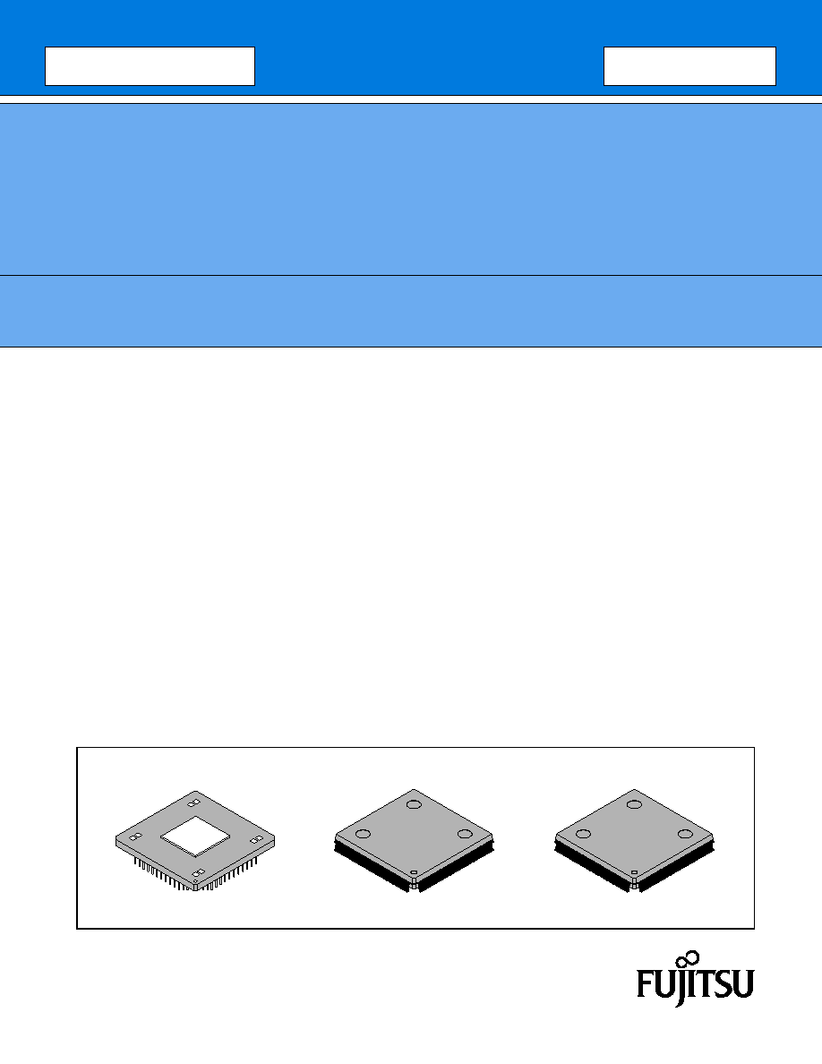
PACKAGE
401-pin Ceramics PGA
208-pin plastic QFP
160-pin plastic QFP
(PGA-401C-A02)
(FPT-208P-M04)
(FPT-160P-M15)

MB91360G Series
2
(Continued)
∑ External bus interface unit with a wide range of functions
Divides the external memory space into a maximum of eight areas. Chip select signal setting, data bus width
selection (8, 16, 32-bit) , and area size can be specified for each area.
∑
Address bus up to 32 bit wide
∑
Programmable auto-wait function
∑ Internal instruction cache
The MB91360G series contains up to 4-Kbyte instruction cache to improve the execution speed of external
programs.
∑
Two-way set associative caching
∑ DMAC
Direct memory access (DMA) can be used to perform various types of data transfer without going via the CPU.
This improves system performance.
∑
Eight channels (including up to 3 external channels)
∑
Three transfer modes supported : single/block, burst, continuous transfer
∑ Power consumption control mechanisms
The MB91360G series contains a number of functions for controlling the operating clock to reduce power
consumption.
∑
Software control : Sleep and stop/real time clock functions
∑
Hardware control : Hardware standby function
∑
Gear (divider) function : The CPU and peripheral clock frequencies can be set independently.
∑ Contains a range of peripheral functions
∑
UART, U-timer
∑
Real Time Clock (with optional subclock operation and subclock calibration module)
∑
Stepper Motor Control
∑
Sound Generator
∑
Serial IO (SIO) , SIO-Prescaler
∑
Power Down Reset
∑
Alarm Comparator
∑
IO-Timer
∑
I
2
C Interface
∑
10 Bit D/A Converter
∑
CAN Interface
∑
10-bit A/D converter
∑
16-bit reload timer
∑
16-bit PWM timer
∑
Watchdog timer
∑
Bit search module
∑
Interrupt controller
∑
External interrupt inputs
∑
I/O port function
∑ Interrupt levels
"16 maskable interrupt levels"
∑ Other
∑
Power supply voltage
∑
5 V power supply used, the internal regulator creates internal supply of 3.3 V
∑
Package : MB91FV360GA uses a PGA401 package, MB91F362GA is delivered in a QFP208 package, and
MB91F369GA in QFP160 package.
MB91360G Series
3
s
PRODUCT LINEUP
Resource Channels
Memory Size
MB91FV360GA
MB91F362GA
MB91F369GA
Cache/Instruction RAM
4 KB / 4 KB
- / 4 KB
- / 4 KB
D-bus RAM
16 KB
12 KB
16 KB
F-bus RAM
16 KB
4 KB
16 KB
Flash/ROM
512 KB on F-bus
512 KB on F-bus
512 KB on F-bus
Boot ROM
2 KB
2 KB
2 KB
CAN
4 ch
3 ch
2 ch
Stepper Motor Control
4 ch
4 ch
Sound Generator
1 ch
1 ch
1 ch
PPG
8 ch
8 ch
4 ch
Input Capture
4 ch
4 ch
Output Compare
4 ch
4 ch
Free Running Timer
2 ch
2 ch
D/A Converter
2 ch
2 ch
A/D Converter
16 ch
16 ch
10 ch
I
2
C 100 kHz
I
2
C 400 kHz
1 ch
1 ch
1 ch
Alarm Comparator
1 ch
1 ch
1 ch
SIO/SIO prescaler
2 ch
2 ch
2 ch
UART/U-Timer
3 ch
3 ch
1 ch
16-bit Reload Timer
6 ch
6 ch
6 ch
Ext. Interrupt
8 ch
8 ch
8 ch
Non maskable Interrupt
1
Real Time Clock
1
1
1
32 kHz subclock option for RTC
yes
no
no
subclock calibration
yes
no
no
LED port
8 bit
8 bit
Power down Reset
1
1
1
Bit search Module
1
1
1
Watchdog timer
1
1
1
Ext. Address Bus
32 bit
21 bit
up to 24 bit
Ext. Data Bus
32 bit
32 bit
32 bit
Ext. DMA
3 ch
1 ch
1 ch
Max operating frequency
64 MHz
64 MHz
64 MHz
MB91360G Series
4
s
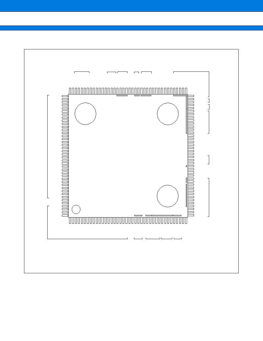
PIN ASSIGNMENTS
∑
∑
∑
∑
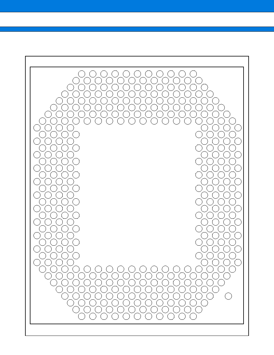
MB91FV360GA
(BOTTOM VIEW)
(PGA-401C-A02)
24
23
25
26
27
28
29
30
31
32
33
70
69
71
72
73
74
75
76
77
78
79
80
120
119
121
122
123
124
125
126
127
128
129
130
131
175
174
176
177
178
179
180
181
182
183
184
185
186
187
231
230
232
233
234
235
236
237
238
239
240
241
242
243
244
284
173
285
286
287
288
289
290
291
292
293
294
295
296
297
188
229
118
334
335
336
337
338
339
340
341
342
343
344
345
346
245
132
172
68
22
117
228
333
67
171
282
379
21
116
227
332
66
170
281
378
20
115
226
331
65
169
280
377
19
114
225
330
64
168
279
376
18
113
224
329
63
167
278
375
17
112
223
328
62
166
277
374
16
111
222
327
61
165
276
373
15
110
221
326
60
164
275
372
14
109
220
325
59
163
274
371
13
108
219
324
58
162
273
370
12
107
218
323
57
161
272
369
368
367
366
365
364
363
362
361
360
359
358
320
319
318
317
316
315
314
313
312
311
310
257
144
201
268
267
266
265
264
263
262
261
260
259
258
212
211
210
209
208
207
206
205
204
203
202
155
154
153
152
151
150
149
148
147
146
145
101
100
99
98
97
96
95
94
93
52
51
50
49
48
47
46
45
7
6
5
4
3
2
1
309
200
92
106
217
322
321
160
271
270
269
216
215
214
213
159
158
157
156
105
104
103
102
56
55
54
53
11
10
9
8
283
380
381
382
383
384
385
386
387
388
389
390
391
298
189
81
347
246
133
34
392
299
190
82
348
247
134
35
393
300
191
83
349
248
135
36
394
301
192
84
350
249
136
37
395
302
193
85
351
250
137
38
396
303
194
86
352
251
138
39
397
304
195
87
353
252
139
40
398
305
196
88
354
253
140
41
399
306
197
89
355
254
141
42
400
307
198
90
356
255
142
43
401
308
199
91
357
256
143
44
INDEX
MB91360G Series
5
∑
∑
∑
∑
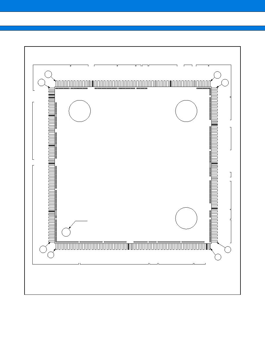
MB91F362GA
(TOP VIEW)
(FPT-208P-M04)
156
157
UART
PQ [5:0]
PP [5:0]
PO [7:0]
PN [5:0] PM [3:0]
P9 [7:0]
P8 [7:0]
P7 [4:6]
P6 [4:0]
P5 [7:0]
P4 [7:0]
P3 [7:0]
P2 [7:0]
P1 [7:0]
P0 [7:0]
PS [7:0]
PR [7:0]
PL [7:0]
PK [7:0]
PJ [7:0]
PI [6:0]
PH [7:0]
PB [2:0]
PG [7:0]
CAN
PPG
SIO
I
2
C
XTAL
+
PLL
OCU
ICU
LED
DAC
ADC
DMA
ADC
53
52
1
208
INDEX
SMC
105
104
SIN2
SOT1
SIN1
SOT0
SIN0
RX2
TX2
RX1
TX1
RX0
TX0
V
SS
V
DD
OCPA7
OCPA6
OCPA5
OCPA4
OCPA3
OCPA2
OCPA1
OCPA0
SCK3
SOT3
SIN3
SCK4
SIN4
SOT4
SCL
SDA
SGA
SGO
VCI
CPO
V
SS
X1A
X0A
X1
X0
V
DD
SELCLK
MONCLK
INITX
HSTX
MD2
MD1
MD0
V
SS
OUT3
OUT2
OUT1
OUT0
IN3
D24
D25
D26
D27
D28
D29
D30
D31
A0
A1
A2
A3
A4
A5
A6
A7
A8
A9
A10
A11
A12
A13
A14
A15
V
DD
V
SS
A16
A17
A18
A19
A20
CS4X
CS5X
CS6X
RDY
BGRNTX
BRQ
RDX
WR0X
WR1X
WR2X
WR3X
AS
ALE
CLK
AH/BOOT
CS0X
CS1X
CS2X
CS3X
V
DD
V
SS
IN2
IN1
IN0
INT7
INT6
INT5
INT4
INT3
INT2
INT1
INT0
V
SS
V
DD
LED7
LED6
LED5
LED4
LED3
LED2
LED1
LED0
LTESTX
CPUTESTX
TESTX
ATGX
V
DD
V
SS
ALARM
DA1
DA0
AV
SS
AN7
AN6
AN5
AN4
AN3
AN2
AN1
AN0
AVRH
AV
CC
DEOP0
DACK0
DREQ0
AN15
AN14
AN13
AN12
AN11
AN10
AN9
AN8
SOT2
V
SS
V
CC
3C
V
DD
HV
SS
PWM1P0
PWM1M0
PWM2P0
PWM2M0
HV
DD
PWM1P1
PWM1M1
PWM2P1
PWM2M1
HV
SS
PWM1P2
PWM1M2
PWM2P2
PWM2M2
HV
DD
PWM1P3
PWM1M3
PWM2P3
PWM2M3
HV
SS
V
DD
D0
D1
D2
D3
D4
D5
D6
D7
D8
D9
D10
D11
D12
D13
D14
V
DD
V
SS
D15
D16
D17
D18
D19
D20
D21
D22
D23
Ext. Interrupt
Ext. Bus Data
Ext. Bus Address
Chip
Select
Ext. Bus Control
Chip
Select
Mode
Sound
Gen.
MB91360G Series
6
∑
∑
∑
∑
MB91F369GA
(TOP VIEW)
(FPT-160P-M15)
P0 [3:0] PQ [1:0] PP [3:0]
PB [2:0]
P8 [7:0]
P7 [6:4]
PN [5:0]
PK [7:0]
PG [1:0]
PH [7:0]
Ext.Bus Control
Osci.
CAN
SIO
Mode
ADC
Ext. Bus Data
VSS
VDD35
RDY
WR0X
WR1X
WR2X
WR3X
VSS
VDD35
VSS
MONCLK
VDD
VSS
X1
X0
VDD
OCPA3
OCPA2
OCPA1
OCPA0
VSS
VDD
SOT0
SIN0
RX1
TX1
RX0
TX0
VSS
VCC3C
VDDI
VDDI
VDDI
VDDI
VSS
SCK3
SOT3
SIN3
SCK4
SIN4
D0
D1
D2
D3
D4
D5
D6
D7
D8
D9
D10
D11
D12
D13
D14
D15
VDD35
VSS
D16
D17
D18
D19
D20
D21
D22
D23
D24
D25
D26
D27
D28
D29
D30
D31
VDD35
VSS
A0
A1
A2
A3
120
117
119
116
118
115
112
113
114
111
99
104
106
101
100
102
103
105
107
108
109
110
95
90
91
92
93
94
96
97
98
A4
A5
A6
A7
A8
A9
A10
A11
VDD35
CLK
VSS
A12
A13
A14
A15
A16
A17
A18
A19
A20
VDD35
VSS
CS4X
CS5X
CS6X
RDX
BGRNTX
BRQ
AS
ALE
AH
CS0X
CS1X
CS2X
CS3X
DREQ0
DACX0
DEOP
VSS
VDD35
1
2
7
6
5
4
3
9
10
8
11
13
12
14
16
15
17
18
19
20
21
30
29
28
27
26
25
24
23
22
40
39
38
37
36
35
34
33
32
31
121
125
130
129
128
123
127
126
124
122
142
141
140
139
137
138
136
135
133
134
132
131
150
149
151
152
148
147
146
145
144
143
159
158
157
154
155
156
153
160
SOT4
SCL
SDA
SGA
SGO
INT7
INT6
INT5
INT4
INT3
INT2
INT1
INT0
VSS
VDD
LTESTX
CPUTESTX
TESTX
INITX
HSTX
MD2
MD1
MD0
ATGX
VDD
VSS
ALARM
AN9
AN8
AN7
AN6
AN5
AN4
AN3
AN2
AN1
AN0
AVSS
AVCC
AVRH
80
76
71
72
73
74
75
77
78
79
61
62
63
64
65
66
67
68
69
70
51
52
53
54
55
56
57
58
59
60
41
42
43
44
45
46
47
48
49
50
81
84
88
89
82
86
83
85
87
PPG
UART
I C
2
Sound
Gen.
Ext.Interrupt
Ext. Bus Address
DMA
Chip
Select
Chip
Select
Ext. Bus
Control
PM [3:0]
P13
MB91360G Series
7
s
PIN DESCRIPTIONS
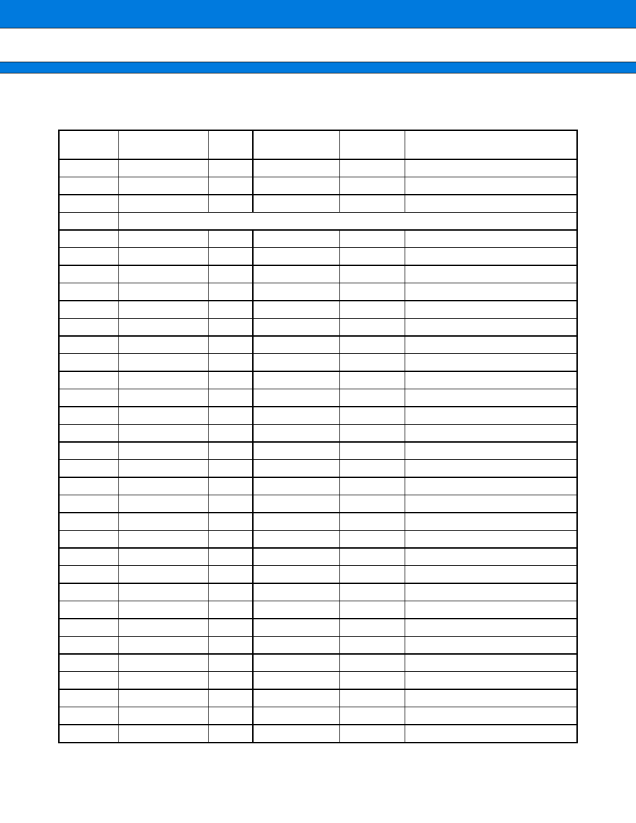
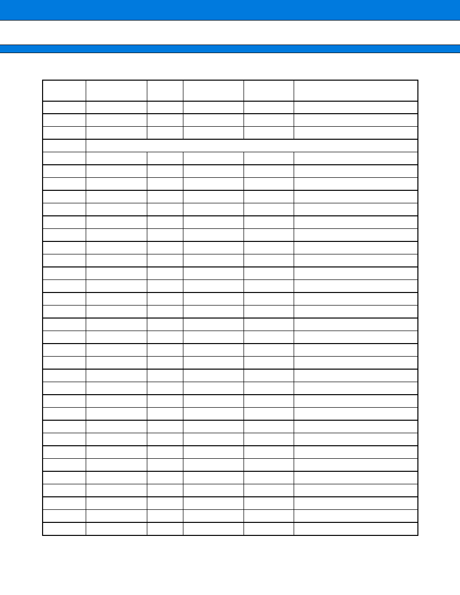
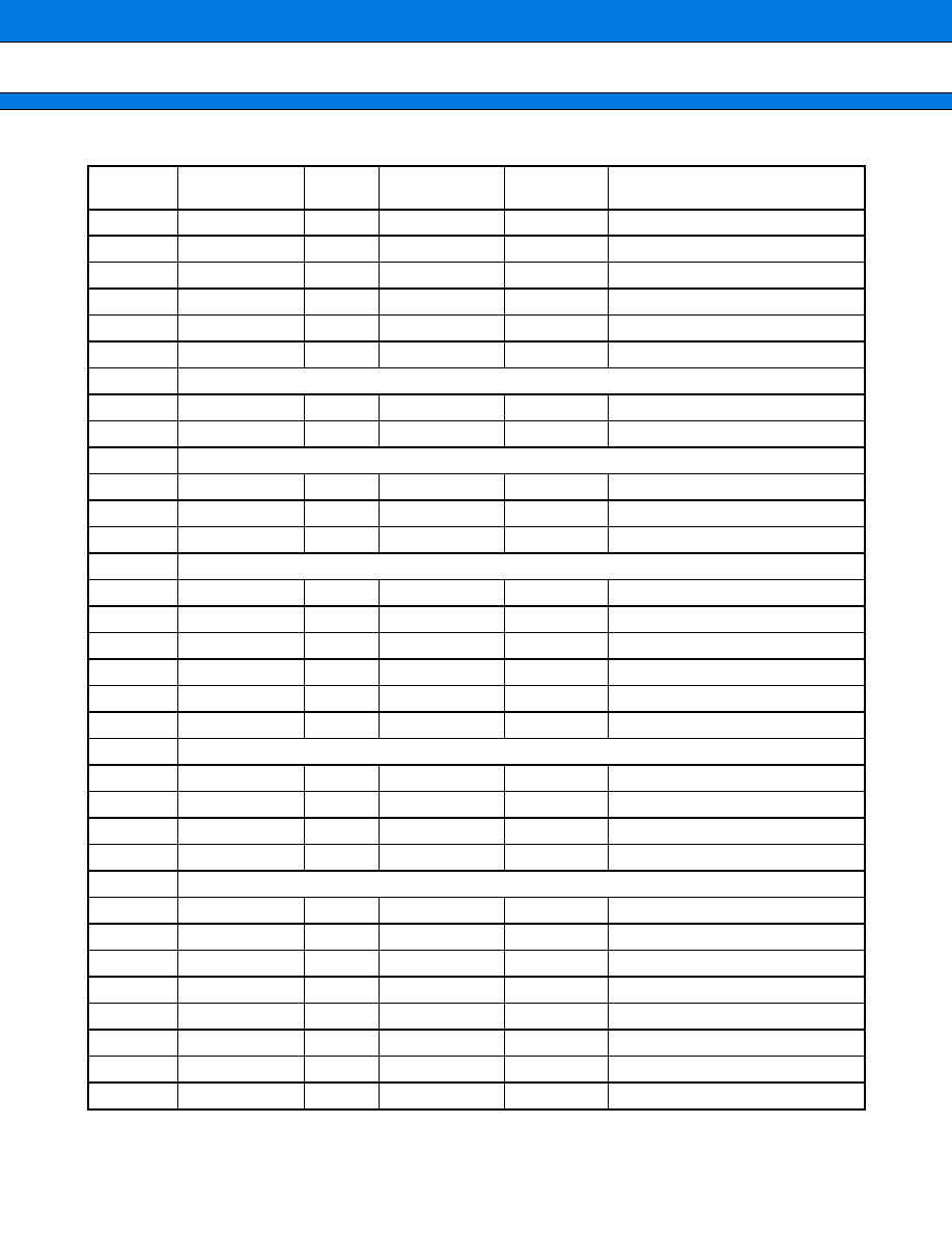
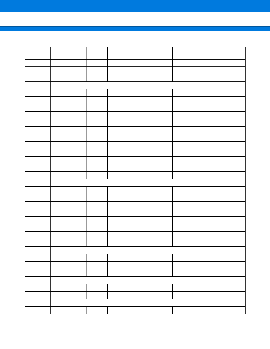
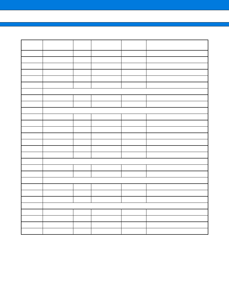
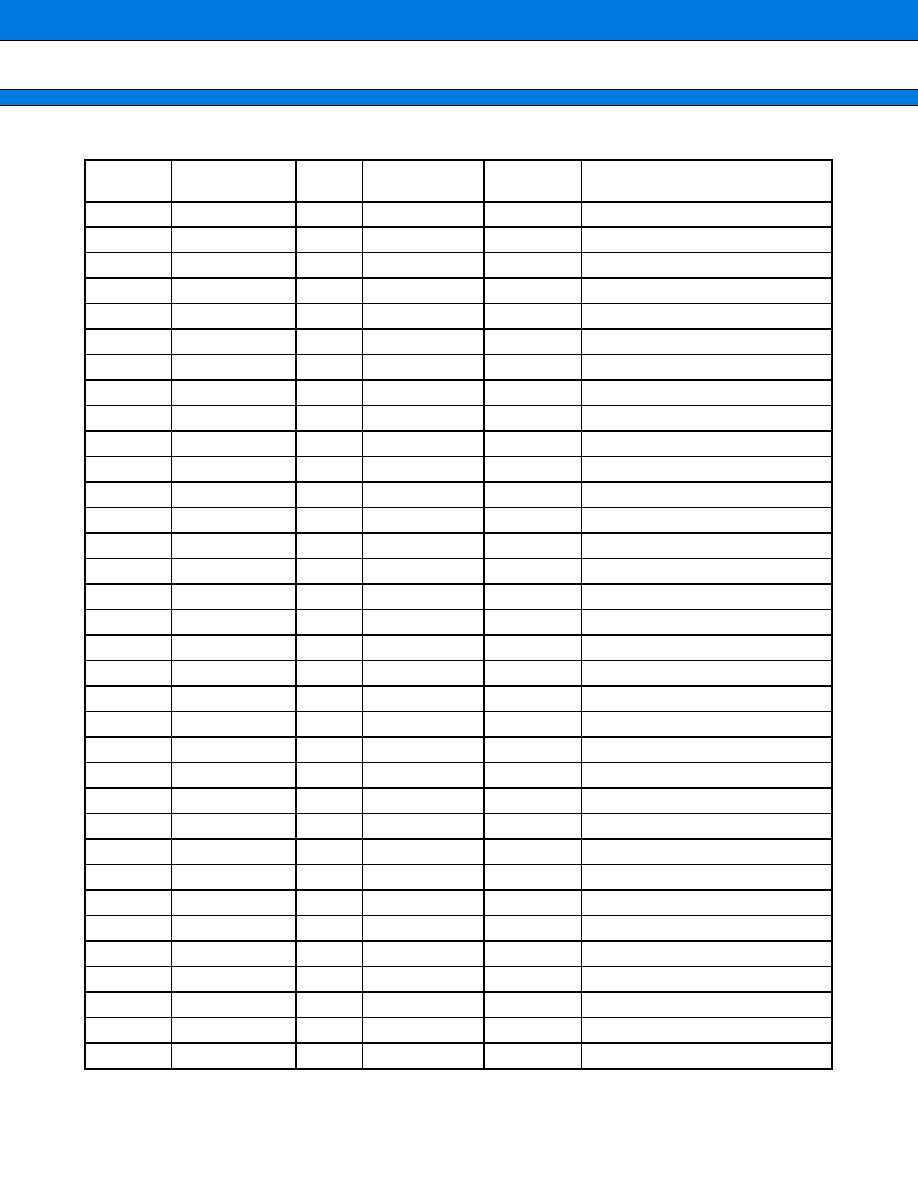
∑ MB91FV360GA I/O Pins and Their Functions
(Continued)
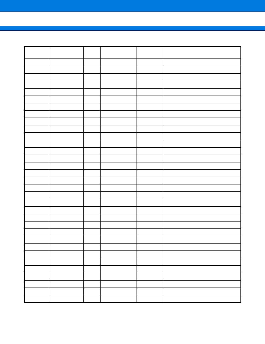
Pin No.
Pin Name
I/O
General
Purpose IO Port
Circuit Type
Function
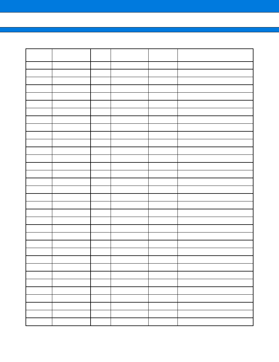
1
D18
I/O
Q
Ext. Bus Data Bit 18
2
D11
I/O
Q
Ext. Bus Data Bit 11
3
D2
I/O
Q
Ext. Bus Data Bit 2
4
not connected
5
HVSS
6
HVDD5B
7
PWM2M1
I/O
PR7
M
SMC 1
8
PWM1M1
I/O
PR5
K
SMC 1
9
PWM1P0
I/O
PR0
K
SMC 0
10
VDD5R
11
VDD5P
12
SCK4
I/O
PN2
A
SIO Clock
13
VDD5J
14
EXRAM
I
P
Trace Control
15
TWRX
O
X
Trace Control
16
TAD9
O
X
Trace Address
17
TAD5
O
X
Trace Address
18
TAD3
O
X
Trace Address
19
TDT68
I/O
W
Trace Data
20
TDT63
I/O
W
Trace Data
21
TDT57
I/O
W
Trace Data
22
TDT49
I/O
W
Trace Data
23
TDT23
I/O
W
Trace Data
24
TDT16
I/O
W
Trace Data
25
TDT7
I/O
W
Trace Data
26
TDT2
I/O
W
Trace Data
27
ICD0
I/O
N
ICE Data
28
ICLK
I/O
L
ICE Clock
29
X0
H
4 MHz Oscillator Pin
30
INTX
I
U
Initial Pin
31
MD1
I
T
Mode Pin 1
32
IN3
I/O
PL3
A
ICU Input 3
33
INT3
I/O
PK3
A
Ext. Interrupt 3
MB91360G Series
8
(Continued)
Pin No.
Pin Name
I/O
General
Purpose IO Port
Circuit Type
Function
34
AN3
I/O
PH3
B
ADC Input 3
35
DACK2
I/O
PB6
A
DMA Acknowledge 2
36
AN13
I/O
PG5
B
ADC Input 13
37
AN8
I/O
PG0
B
ADC Input 8
38
ALE
I/O
P91
A
Ext. Bus Control
39
WR1X
I/O
P85
S
Ext. Bus Control
40
RDX
I/O
P83
S
Ext. Bus Control
41
CS7X
I/O
A
Chip Select 7 (CANs)
42
A26
I/O
Q
Ext. Bus Address Bit 26
43
A20
I/O
Q
Ext. Bus Address Bit 20
44
A12
I/O
Q
Ext. Bus Address Bit 12
45
D21
I/O
Q
Ext. Bus Data Bit 21
46
D16
I/O
Q
Ext. Bus Data Bit 16
47
D13
I/O
Q
Ext. Bus Data Bit 13
48
D7
I/O
Q
Ext. Bus Data Bit 7
49
D3
I/O
Q
Ext. Bus Data Bit 3
50
VSS
51
PWM2P2
I/O
PS2
K
SMC 2
52
PWM2P1
I/O
PR6
K
SMC 1
53
PWM1P1
I/O
PR4
K
SMC 1
54
not connected
55
SIN1
I/O
PQ2
A
UART 1 Input
56
TX3
I/O
PP6
Q
CAN 3 TX
57
SOT3
I/O
PN4
A
SIO Output
58
SOT4
I/O
PN0
A
SIO Output
59
not connected
60
not connected
61
SGO
I/O
PM0
A
Sound Generator SGO
62
TOEX
O
X
Trace Control
63
TAD8
O
X
Trace Address
64
TAD2
O
X
Trace Address
65
TDT67
I/O
W
Trace Data
66
TDT60
I/O
W
Trace Data
MB91360G Series
9
(Continued)
Pin No.
Pin Name
I/O
General
Purpose IO Port
Circuit Type
Function
67
TDT54
I/O
W
Trace Data
68
TDT48
I/O
W
Trace Data
69
TDT26
I/O
W
Trace Data
70
TDT21
I/O
W
Trace Data
71
TDT18
I/O
W
Trace Data
72
TDT12
I/O
W
Trace Data
73
TDT8
I/O
W
Trace Data
74
TDT3
I/O
W
Trace Data
75
ICS2
O
G
ICE Status
76
VDD5F
77
RSTX
I
E
Reset Pin
78
OUT2
I/O
PL6
A
OCU Output 2
79
IN0
I/O
PL0
A
ICU Input 0
80
INT2
I/O
PK2
A
Ext. Interrupt 2
81
AN6
I/O
PH6
B
ADC Input 6
82
AN1
I/O
PH1
B
ADC Input 1
83
AVCC
Analog VCC
84
DEOP0
I/O
PB2
A
DMA EOP 0
85
AN14
I/O
PG6
B
ADC Input 14
86
AN9
I/O
PG1
B
ADC Input 9
87
AS
I/O
P90
A
Ext. Bus Control
88
BRQ
I/O
P82
A
Ext. Bus Control
89
CS6X
I/O
P76
A
Chip Select 6
90
A23
I/O
Q
Ext. Bus Address Bit 23
91
A17
I/O
Q
Ext. Bus Address Bit 17
92
A11
I/O
Q
Ext. Bus Address Bit 11
93
D27
I/O
Q
Ext. Bus Data Bit 27
94
D22
I/O
Q
Ext. Bus Data Bit 22
95
D17
I/O
Q
Ext. Bus Data Bit 17
96
D6
I/O
Q
Ext. Bus Data Bit 16
97
VDD5S
98
PWM1M3
I/O
PS5
K
SMC 3
99
PWM2M3
I/O
PS7
M
SMC 3
100
HVDD5A
MB91360G Series
10
(Continued)
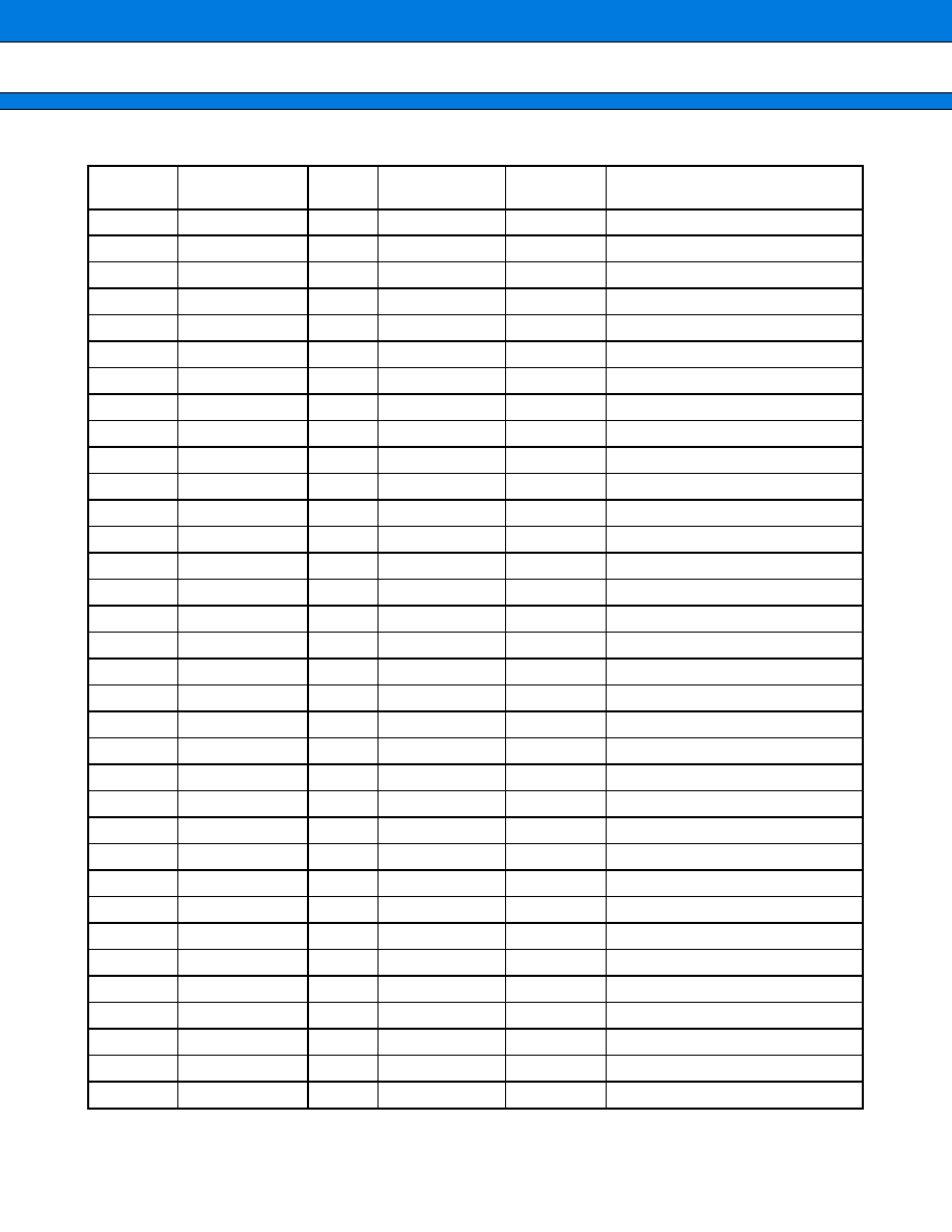
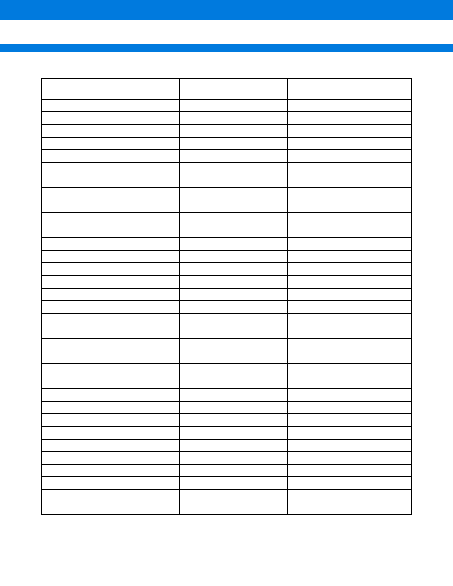
Pin No.
Pin Name
I/O
General
Purpose IO Port
Circuit Type
Function
101
PWM2P0
I/O
PR2
K
SMC0
102
VCC3/C
C
Bypass Capacitor Pin
103
SOT1
I/O
PQ3
A
UART 1 Output
104
SIN0
I/O
PQ0
A
UART 0 Input
105
TX1
I/O
PP2
Q
CAN 1 TX
106
OCPA2
I/O
PO2
A
PPG Output
107
SCK3
I/O
PN5
A
SIO Clock
108
SIN4
I/O
PN1
A
SIO Input
109
SCL
I/O
PM3
Y
I
2
C SCL
110
TCLK
I/O
W
Trace Control
111
TAD12
O
X
Trace Address
112
TAD15
O
X
Trace Address
113
TAD1
O
X
Trace Address
114
TDT65
I/O
W
Trace Data
115
TDT59
I/O
W
Trace Data
116
TDT55
I/O
W
Trace Data
117
TDT51
I/O
W
Trace Data
118
TDT42
I/O
W
Trace Data
119
TDT32
I/O
W
Trace Data
120
TDT27
I/O
W
Trace Data
121
TDT22
I/O
W
Trace Data
122
TDT11
I/O
W
Trace Data
123
TDT4
I/O
W
Trace Data
124
ICD3
I/O
N
ICE Data
125
TDT1
I/O
W
Trace Data
126
SELCLK
I
F
Clock Selection
127
NMIX
I
E
Non maskable Interrupt
128
OUT1
I/O
PL5
A
OCU Output 1
129
IN1
I/O
PL1
A
ICU Input 1
130
INT5
I/O
PK5
A
Ext. Interrupt 5
131
LED4
I/O
PJ4
J
LED Port 4
132
ALARM
I
D
Alarm Comparator Input
133
AN7
I/O
PH7
B
ADC Input 7
134
AN2
I/O
PH2
B
ADC Input 2
MB91360G Series
11
(Continued)
Pin No.
Pin Name
I/O
General
Purpose IO Port
Circuit Type
Function
135
DACK0
I/O
PB1
A
DMA acknowledge 0
136
AN10
I/O
PG2
B
ADC Input 10
137
CS0X
I/O
P94
A
Chip select 0
138
CS3X
I/O
P97
A
Chip select 3
139
BGRNTX
I/O
P81
A
Ext. Bus Control
140
CS4X
I/O
P74
A
Chip select 4
141
A22
I/O
Q
Ext. Bus Address Bit 22
142
A18
I/O
Q
Ext. Bus Address Bit 18
143
A14
I/O
Q
Ext. Bus Address Bit 14
144
A5
I/O
Q
Ext. Bus Address Bit 5
145
INDEX
146
D30
I/O
Q
Ext. Bus Data Bit 30
147
D26
I/O
Q
Ext. Bus Data Bit 26
148
D19
I/O
Q
Ext. Bus Data Bit 19
149
D10
I/O
Q
Ext. Bus Data Bit 10
150
D9
I/O
Q
Ext. Bus Data Bit 9
151
D5
I/O
Q
Ext. Bus Data Bit 5
152
PWM2M2
I/O
PS3
M
SMC 2
153
PWM1P3
I/O
PS4
K
SMC 3
154
PWM2M0
I/O
PR3
M
SMC 0
155
VSS
156
SOT2
I/O
PQ5
A
UART 2 Output
157
SOT0
I/O
PQ1
A
UART 0 Output
158
VDD5O
159
OCPA7
I/O
PO7
A
PPG Output
160
OCPA5
I/O
PO5
A
PPG Output
161
OCPA1
I/O
PO1
A
PPG Output
162
VDD5K
163
X1A
O
I
32 kHz Oscillator Pin
164
X0A
I
I
32 kHz Oscillator Pin
165
SDA
I/O
PM2
Y
I
2
C SDA
166
TAD10
O
X
Trace Address
167
TAD11
O
X
Trace Address
168
TDT66
I/O
W
Trace Data

MB91360G Series
12
(Continued)
Pin No.
Pin Name
I/O
General
Purpose IO Port
Circuit Type
Function
169
TDT61
I/O
W
Trace Data
170
TDT58
I/O
W
Trace Data
171
TDT52
I/O
W
Trace Data
172
TDT45
I/O
W
Trace Data
173
TDT39
I/O
W
Trace Data
174
TDT35
I/O
W
Trace Data
175
TDT31
I/O
W
Trace Data
176
TDT24
I/O
W
Trace Data
177
TDT15
I/O
W
Trace Data
178
TDT14
I/O
W
Trace Data
179
TDT10
I/O
W
Trace Data
180
ICD1
I/O
N
ICE Data
181
ICD2
I/O
N
ICE Data
182
HSTX
I
E
Hardware Standby
183
OUT3
I/O
PL7
A
OCU Output 3
184
OUT0
I/O
PL4
A
OCU Output 0
185
INT6
I/O
PK6
A
Ext. Interrupt 6
186
LED7
I/O
PJ7
J
LED Port 7
187
LED1
I/O
PJ1
J
LED Port 1
188
CPUTESTX
I
E
Test Input
189
DA1
O
C
DAC Output
190
AN4
I/O
PH4
B
ADC Input 4
191
DEOP1
I/O
PB5
A
DMA EOP 1
192
DACK1
I/O
PB4
A
DMA Acknowledge 1
193
DREQ0
I/O
PB0
A
DMA Request 0
194
CLK
I/O
P92
A
Ext. Bus Clock
195
AH/BOOT
I/O
P93
A
Ext. Bus Control/Boot Signal
196
CS5X
I/O
P75
A
Chip Select 5
197
A24
I/O
Q
Ext. Bus Address Bit 24
198
A21
I/O
Q
Ext. Bus Address Bit 21
199
A15
I/O
Q
Ext. Bus Address Bit 15
200
A8
I/O
Q
Ext. Bus Address Bit 8
201
A2
I/O
Q
Ext. Bus Address Bit 2
202
A0
I/O
Q
Ext. Bus Address Bit 0
MB91360G Series
13
(Continued)
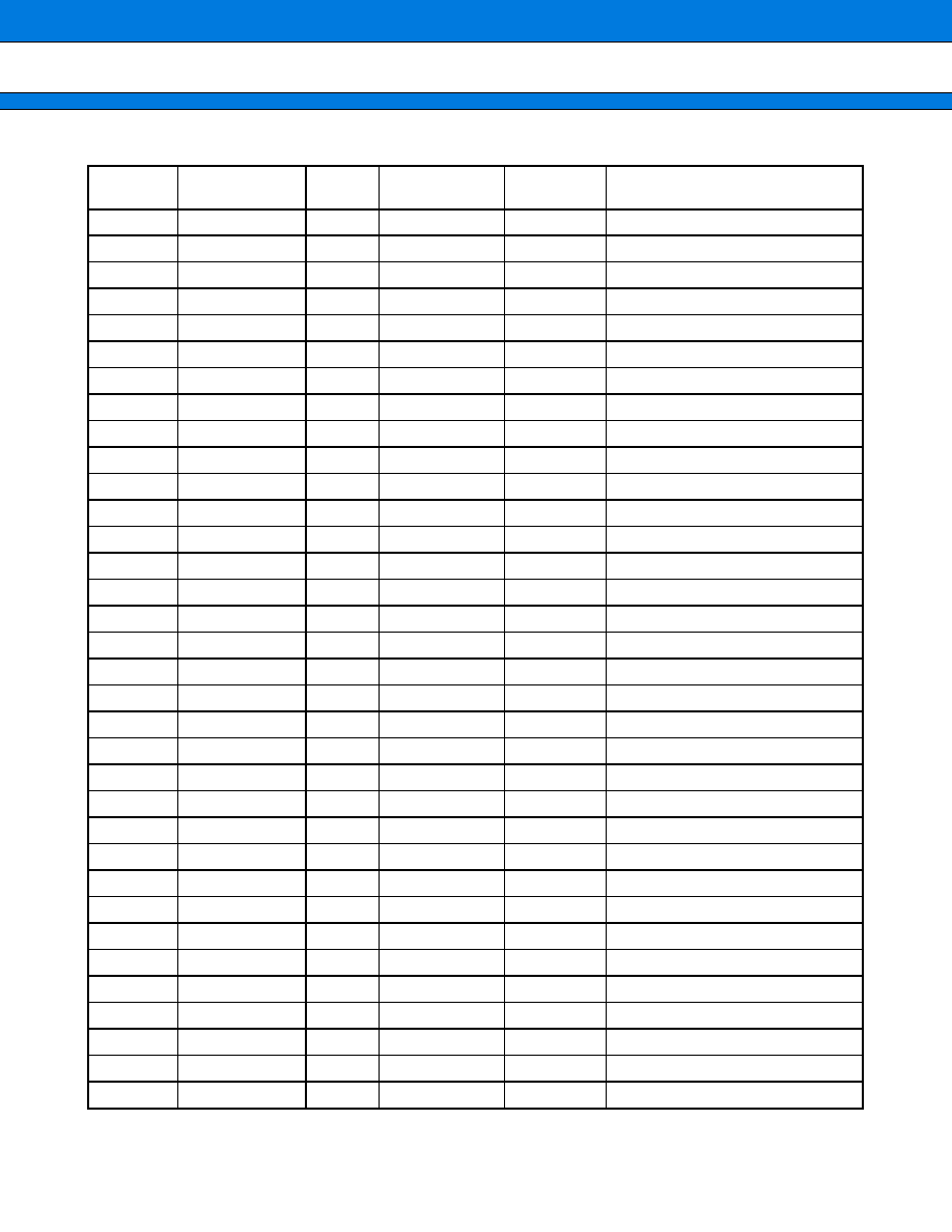
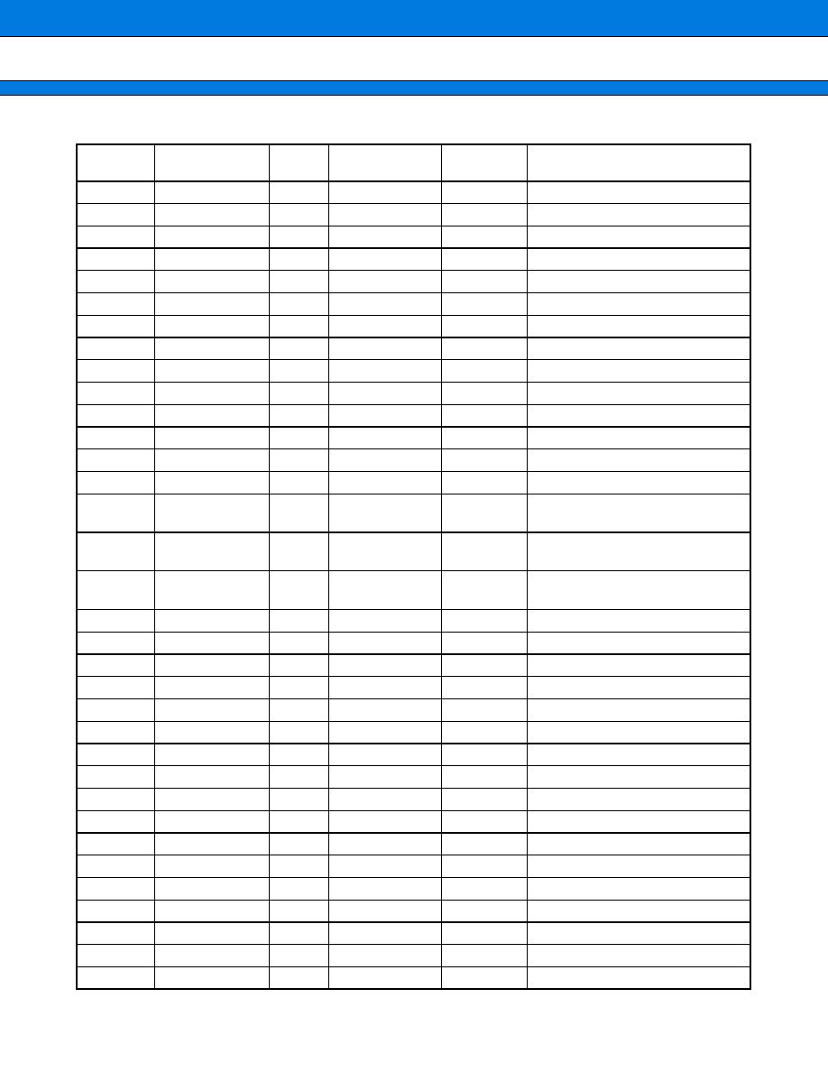
Pin No.
Pin Name
I/O
General
Purpose IO Port
Circuit Type
Function
203
D29
I/O
Q
Ext. Bus Address Bit 29
204
D25
I/O
Q
Ext. Bus Address Bit 25
205
D20
I/O
Q
Ext. Bus Address Bit 20
206
D15
I/O
Q
Ext. Bus Address Bit 15
207
D4
I/O
Q
Ext. Bus Address Bit 4
208
HVDD5C
209
PWM1M2
I/O
PS1
K
SMC2
210
PWM1P2
I/O
PS0
K
SMC2
211
PWM1M0
I/O
PR1
K
SMC0
212
SIN2
I/O
PQ4
A
UART 2 Input
213
RX3
I/O
PP7
Q
CAN 3 RX
214
VSS
215
RX0
I/O
PP1
Q
CAN 0 RX
216
VDD5N
217
OCPA4
I/O
PO4
A
PPG Output
218
OCPA0
I/O
PO0
A
PPG Output
219
SIN3
I/O
PN3
A
SIO Input
220
VSS
221
SGA
I/O
PM1
A
Sound Generator SGA
222
TAD13
O
X
Trace Address
223
TAD7
O
X
Trace Address
224
TAD6
O
X
Trace Address
225
TDT64
I/O
W
Trace Data
226
TDT56
I/O
W
Trace Data
227
TDT50
I/O
W
Trace Data
228
TDT44
I/O
W
Trace Data
229
TDT41
I/O
W
Trace Data
230
TDT37
I/O
W
Trace Data
231
TDT34
I/O
W
Trace Data
232
TDT30
I/O
W
Trace Data
233
TDT25
I/O
W
Trace Data
234
TDT20
I/O
W
Trace Data
235
TDT9
I/O
W
Trace Data
236
BREAK
I
O
ICE Break
MB91360G Series
14
(Continued)
Pin No.
Pin Name
I/O
General
Purpose IO Port
Circuit Type
Function
237
ICS1
O
G
ICE Status
238
ICS0
O
G
ICE Status
239
MD2
I
T
Mode Pin 2
240
IN2
I/O
PL2
A
ICU Input 2
241
INT4
I/O
PK4
A
Ext. Interrupt 4
242
LED6
I/O
PJ6
J
LED Port 6
243
LED3
I/O
PJ3
J
LED Port 3
244
not connected
245
TESTX
I
E
Test Input
246
DA0
O
C
DAC Output
247
AN5
I/O
PH5
B
ADC Input 5
248
AN0
I/O
PH0
B
ADC Input 0
249
AN15
I/O
PG7
B
ADC Input 15
250
CS1X
I/O
P95
A
Chip select 1
251
WR3X
I/O
P87
S
Ext. Bus Control
252
WR2X
I/O
P86
S
Ext. Bus Control
253
DREQ2
I/O
P73
A
DMA Request 2
254
A19
I/O
Q
Ext. Bus Address Bit 19
255
A13
I/O
Q
Ext. Bus Address Bit 13
256
A7
I/O
Q
Ext. Bus Address Bit 7
257
A4
I/O
Q
Ext. Bus Address Bit 4
258
D31
I/O
Q
Ext. Bus Data Bit 31
259
D28
I/O
Q
Ext. Bus Data Bit 28
260
D23
I/O
Q
Ext. Bus Data Bit 23
261
D14
I/O
Q
Ext. Bus Data Bit 14
262
D8
I/O
Q
Ext. Bus Data Bit 8
263
D1
I/O
Q
Ext. Bus Data Bit 1
264
D0
I/O
Q
Ext. Bus Data Bit 0
265
not connected
266
HVSS
267
not connected
268
VSS
269
RX2
I/O
PP5
Q
CAN 2 RX
270
RX1
I/O
PP3
Q
CAN 1 RX
MB91360G Series
15
(Continued)
Pin No.
Pin Name
I/O
General
Purpose IO Port
Circuit Type
Function
271
VSS
272
OCPA3
I/O
PO3
A
PPG Output
273
VSS
274
not connected
275
VDD5I
276
TADSCX
O
X
Trace Control
277
TCE1X
O
X
Trace Control
278
TAD4
O
X
Trace Address
279
TAD0
O
X
Trace Address
280
TDT62
I/O
W
Trace Data
281
TDT53
I/O
W
Trace Data
282
TDT47
I/O
W
Trace Data
283
TDT43
I/O
W
Trace Data
284
TDT36
I/O
W
Trace Data
285
TDT33
I/O
W
Trace Data
286
TDT28
I/O
W
Trace Data
287
TDT19
I/O
W
Trace Data
288
TDT13
I/O
W
Trace Data
289
TDT6
I/O
W
Trace Data
290
TDT5
I/O
W
Trace Data
291
X1
H
4 MHz Oscillator Pin
292
MONCLK
O
G
Clock Output for test purposes
293
MD0
I
T
Mode Pin 0
294
INT7
I/O
PK7
A
Ext. Interrupt 7
295
INT1
I/O
PK1
A
Ext. Interrupt 1
296
LED5
I/O
PJ5
J
LED Port 5
297
LTESTX
I
E
Test Input
298
ATGX
I/O
PI3
A
Analog Reference Low
299
AVRL
R
Analog Reference High
300
AVRH
R
DMA Request 1
301
DREQ1
I/O
PB3
A
ADC Input 12
302
AN12
I/O
PG4
B
ADC Input 11
303
AN11
I/O
PG3
B
Ext. Bus Control
304
WR0X
I/O
P84
S
Ext. Bus Control
MB91360G Series
16
(Continued)
Pin No.
Pin Name
I/O
General
Purpose IO Port
Circuit Type
Function
305
RDY
I/O
S
Ext. Bus Control
306
A25
I/O
Q
Ext. Bus Address Bit 25
307
A16
I/O
Q
Ext. Bus Address Bit 16
308
A10
I/O
Q
Ext. Bus Address Bit 10
309
A6
I/O
Q
Ext. Bus Address Bit 6
310
A1
I/O
Q
Ext. Bus Address Bit 1
311
not connected
312
D24
I/O
Q
Ext. Bus Data Bit 24
313
D12
I/O
Q
Ext. Bus Data Bit 12
314
not connected
315
PWM2P3
I/O
PS6
K
SMC 3
316
HVSS
317
HVSS
318
not connected
319
VDD5Q
320
TX2
I/O
PP4
Q
CAN 2 TX
321
TX0
I/O
PP0
Q
CAN 0 TX
322
OCPA6
I/O
PO6
A
PPG Output
323
VDD5M
324
VDD5L
325
not connected
326
VDD5H
327
TAD14
O
X
Trace Address
328
VSS3
329
VSS3
330
not connected
331
VDD3C
332
TDT46
I/O
W
Trace Data
333
TDT40
I/O
W
Trace Data
334
TDT38
I/O
W
Trace Data
335
VDD3B
336
TDT29
I/O
W
Trace Data
337
TDT17
I/O
W
Trace Data
338
VDD3A
MB91360G Series
17
(Continued)
Pin No.
Pin Name
I/O
General
Purpose IO Port
Circuit Type
Function
339
TDT0
I/O
W
Trace Data
340
VSS
341
VSS
342
not connected
343
VDD5E
344
INT0
I/O
PK0
A
Ext. Interrupt 0
345
LED2
I/O
PJ2
J
LED Port 2
346
LED0
I/O
PJ0
J
LED Port 0
347
VDD5D
348
AVSS
Analog VSS
349
DEOP2
I/O
PB7
A
DMA EOP 2
350
VDD5C
351
CS2X
I/O
P96
A
Chip select 2
352
VSS
353
VSS
354
VDD5B
355
not connected
356
A9
I/O
Q
Ext. Bus Address Bit 9
357
A3
I/O
Q
Ext. Bus Address Bit 3
358
VSS
359
VSS
360
VDD5T
361
VSS
362
VSS
363
VSS
364
not connected
365
HVSS
366
VSS
367
VSS
368
not connected
369
VSS
370
VSS
371
not connected
372
VSS
MB91360G Series
18
(Continued)
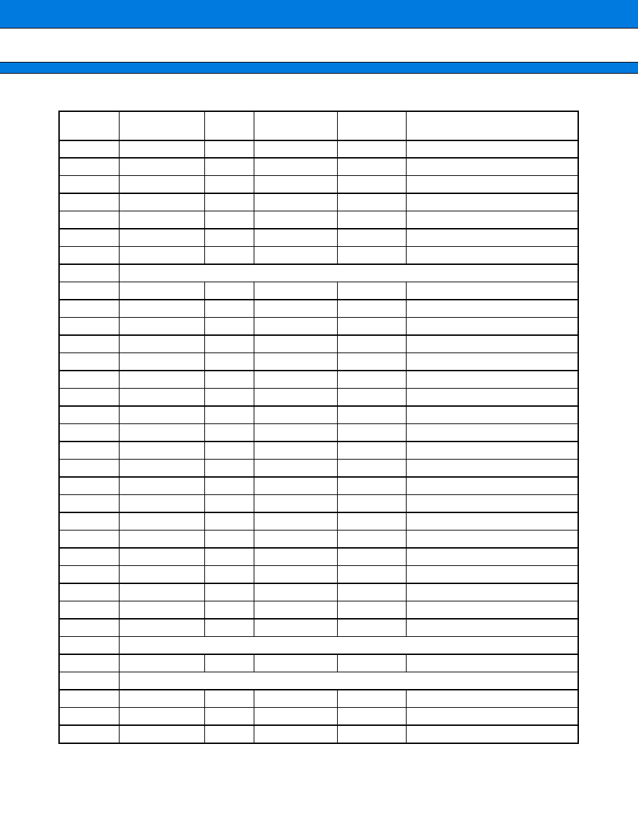
Pin No.
Pin Name
I/O
General
Purpose IO Port
Circuit Type
Function
373
VSS
374
VSS
375
VDD3D
376
VSS3
377
VSS3
378
VSS3
379
not connected
380
VSS3
381
VSS3
382
not connected
383
VSS3
384
VSS3
385
VSS3
386
VDD5G
387
VSS
388
VSS
389
VSS
390
not connected
391
VSS
392
VSS
393
not connected
394
VSS
395
VSS
396
VSS
397
not connected
398
VSS
399
VSS
400
VSS
401
VDD5A
MB91360G Series
19
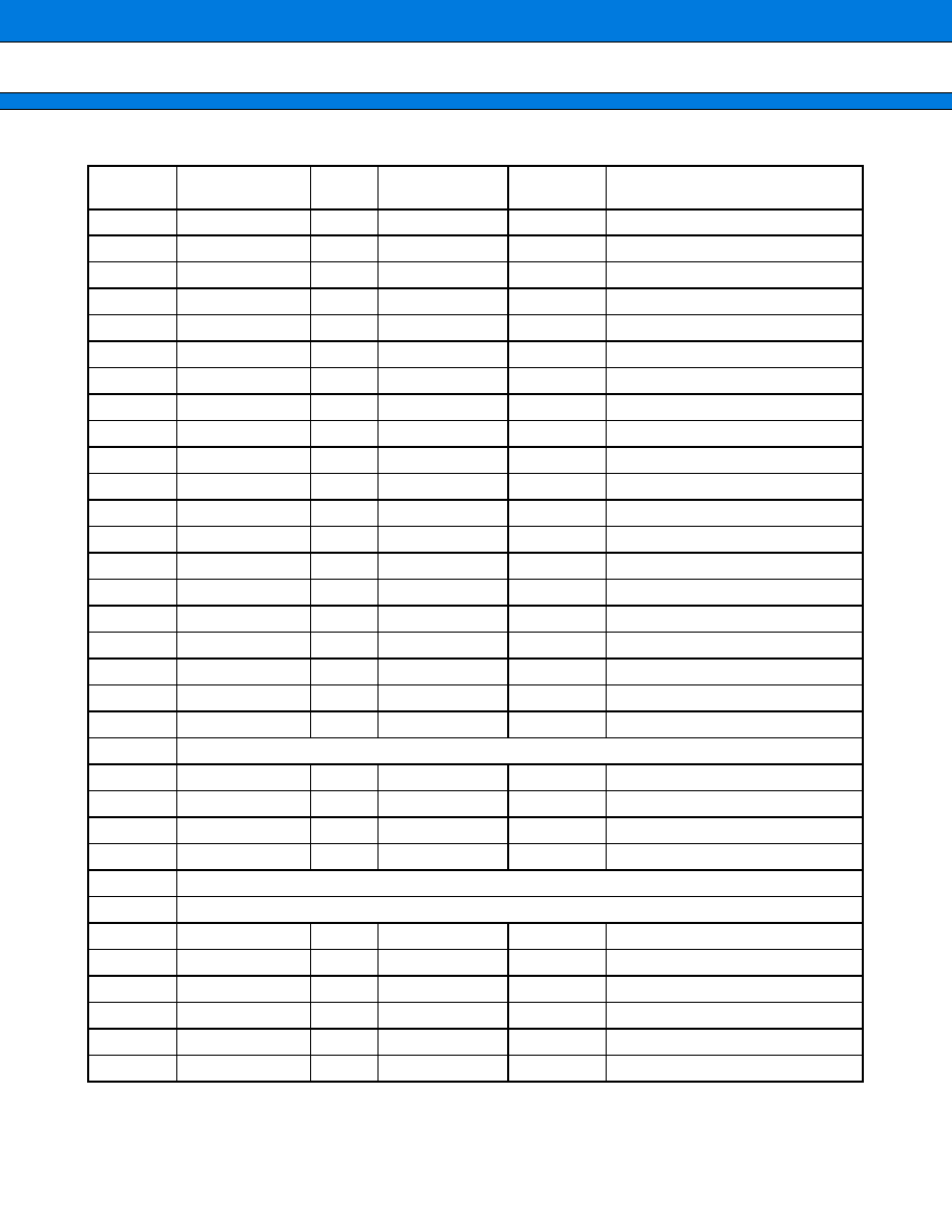
∑ MB91FV362GA I/O Pins and Their Functions
(Continued)
Pin No.
Pin Name
I/O
General
Purpose IO Port
Circuit Type
Function
1
D24
I/O
Q
Ext. Bus Data Bit 24
2
D25
I/O
Q
Ext. Bus Data Bit 25
3
D26
I/O
Q
Ext. Bus Data Bit 26
4
D27
I/O
Q
Ext. Bus Data Bit 27
5
D28
I/O
Q
Ext. Bus Data Bit 28
6
D29
I/O
Q
Ext. Bus Data Bit 29
7
D30
I/O
Q
Ext. Bus Data Bit 30
8
D31
I/O
Q
Ext. Bus Data Bit 31
9
A0
I/O
Q
Ext. Bus Address Bit 0
10
A1
I/O
Q
Ext. Bus Address Bit 1
11
A2
I/O
Q
Ext. Bus Address Bit 2
12
A3
I/O
Q
Ext. Bus Address Bit 3
13
A4
I/O
Q
Ext. Bus Address Bit 4
14
A5
I/O
Q
Ext. Bus Address Bit 5
15
A6
I/O
Q
Ext. Bus Address Bit 6
16
A7
I/O
Q
Ext. Bus Address Bit 7
17
A8
I/O
Q
Ext. Bus Address Bit 8
18
A9
I/O
Q
Ext. Bus Address Bit 9
19
A10
I/O
Q
Ext. Bus Address Bit 10
20
A11
I/O
Q
Ext. Bus Address Bit 11
21
A12
I/O
Q
Ext. Bus Address Bit 12
22
A13
I/O
Q
Ext. Bus Address Bit 13
23
A14
I/O
Q
Ext. Bus Address Bit 14
24
A15
I/O
Q
Ext. Bus Address Bit 15
25
VDD35
Separated Ext. Bus VDD, 3.3 V or 5.0 V
26
VSS
27
A16
I/O
Q
Ext. Bus Address Bit 16
28
A17
I/O
Q
Ext. Bus Address Bit 17
29
A18
I/O
Q
Ext. Bus Address Bit 18
30
A19
I/O
Q
Ext. Bus Address Bit 19
31
A20
I/O
Q
Ext. Bus Address Bit 20
32
CS4X
I/O
P74
A
Chip select 4
33
CS5X
I/O
P75
A
Chip select 5
MB91360G Series
20
(Continued)
Pin No.
Pin Name
I/O
General
Purpose IO Port
Circuit Type
Function
34
CS6X
I/O
P76
A
Chip select 6
35
RDY
I/O
S
Ext. Bus Control
36
BGRNT
I/O
P81
A
Ext. Bus Control
37
BRQ
I/O
P82
A
Ext. Bus Control
38
RDX
I/O
S
Ext. Bus Control
39
WR0X
I/O
S
Ext. Bus Control
40
WR1X
I/O
S
Ext. Bus Control
41
WR2X
I/O
S
Ext. Bus Control
42
WR3X
I/O
S
Ext. Bus Control
43
AS
I/O
P90
A
Ext. Bus Control
44
ALE
I/O
P91
A
Ext. Bus Control
45
CLK
I/O
A
Ext. Bus Clock
46
AH
I/O
P93
A
Ext. Bus Control Signal
47
CS0X
I/O
P94
A
Chip select 0
48
CS1X
I/O
P95
A
Chip select 1
49
CS2X
I/O
P96
A
Chip select 2
50
CS3X
I/O
P97
A
Chip select 3
51
VDD35
separated Ext. Bus VDD, 3.3 or 5.0 V
52
VSS
53
AN8
I/O
PG0
B
ADC Input 8
54
AN9
I/O
PG1
B
ADC Input 9
55
AN10
I/O
PG2
B
ADC Input 10
56
AN11
I/O
PG3
B
ADC Input 11
57
AN12
I/O
PG4
B
ADC Input 12
58
AN13
I/O
PG5
B
ADC Input 13
59
AN14
I/O
PG6
B
ADC Input 14
60
AN15
I/O
PG7
B
ADC Input 15
61
DREQ0
I/O
PB0
A
DMR Request 0
62
DACK0
I/O
PB1
A
DMA Acknowledge 0
63
DEOP0
I/O
PB2
A
DMA EOP 0
64
AVCC
Analog VCC
65
AVRH
R
Analog Reference High
66
AN0
I/O
PH0
B
ADC Input 0
MB91360G Series
21
(Continued)
Pin No.
Pin Name
I/O
General
Purpose IO Port
Circuit Type
Function
67
AN1
I/O
PH1
B
ADC Input 1
68
AN2
I/O
PH2
B
ADC Input 2
69
AN3
I/O
PH3
B
ADC Input 3
70
AN4
I/O
PH4
B
ADC Input 4
71
AN5
I/O
PH5
B
ADC Input 5
72
AN6
I/O
PH6
B
ADC Input 6
73
AN7
I/O
PH7
B
ADC Input 7
74
AVSS, AVRL
Analog VSS, Analog Reference Low
75
DA0
O
C
DAC Output
76
DA1
O
C
DAC Output
77
ALARM
I
D
Alarm Comparator Input
78
VSS
79
VDD
80
ATGX
I/O
PI3
A
ADC Trigger Input
81
TESTX
I
E
Test Input
(should be connected to VDD)
82
CPUTESTX
I
E
Test Input
(should be connected to VDD)
83
LTESTX
I
E
Test Input
(should be connected to VDD)
84
LED0
I/O
PJ0
J
LED Port 0
85
LED1
I/O
PJ1
J
LED Port 1
86
LED2
I/O
PJ2
J
LED Port 2
87
LED3
I/O
PJ3
J
LED Port 3
88
LED4
I/O
PJ4
J
LED Port 4
89
LED5
I/O
PJ5
J
LED Port 5
90
LED6
I/O
PJ6
J
LED Port 6
91
LED7
I/O
PJ7
J
LED Port 7
92
VDD
93
VSS
94
INT0
I/O
PK0
A
Ext. Interrupt 0
95
INT1
I/O
PK1
A
Ext. Interrupt 1
96
INT2
I/O
PK2
A
Ext. Interrupt 2
97
INT3
I/O
PK3
A
Ext. Interrupt 3
98
INT4
I/O
PK4
A
Ext. Interrupt 4
99
INT5
I/O
PK5
A
Ext. Interrupt 5
100
INT6
I/O
PK6
A
Ext. Interrupt 6
MB91360G Series
22
(Continued)
Pin No.
Pin Name
I/O
General
Purpose IO Port
Circuit Type
Function
101
INT7
I/O
PK7
A
Ext. Interrupt 7
102
IN0
I/O
PL0
A
ICU Input 0
103
IN1
I/O
PL1
A
ICU Input 1
104
IN2
I/O
PL2
A
ICU Input 2
105
IN3
I/O
PL3
A
ICU Input 3
106
OUT0
I/O
PL4
A
OCU Output 0
107
OUT1
I/O
PL5
A
OCU Output 1
108
OUT2
I/O
PL6
A
OCU Output 2
109
OUT3
I/O
PL7
A
OCU Output 3
110
VSS
111
MD0
I
T
Mode Pin 0
112
MD1
I
T
Mode Pin 1
113
MD2
I
T
Mode Pin 2
114
HSTX
I
E
Hardware Standby
115
INITX
I
U
Initial Pin
116
MONCLK
O
G
System Clock Output for evaluation
purposes
117
SELCLK
I
F
Clock Selection, must be connected
to VDD
118
VDD
119
X0
H
4 MHz Oscillator Pin
120
X1
H
4 MHz Oscillator Pin
121
X0A
I
I
reserved-must be connected to VSS
122
X1A
O
I
reserved-should be left open
123
VSS
124
CPO
C
reserved-should be left open
125
VCI
D
reserved-must be connected to VSS
126
SGO
I/O
PM0
A
Sound Generator SGO
127
SGA
I/O
PM1
A
Sound Generator SGA
128
SDA
I/O
PM2
Y
I
2
C SDA
129
SCL
I/O
PM3
Y
I
2
C SCL
130
SOT4
I/O
PN0
A
SIO Output
131
SIN4
I/O
PN1
A
SIO Input
132
SCK4
I/O
PN2
A
SIO Clock
133
SIN3
I/O
PN3
A
SIO Input
134
SOT3
I/O
PN4
A
SIO Output

MB91360G Series
23
(Continued)
Pin No.
Pin Name
I/O
General
Purpose IO Port
Circuit Type
Function
135
SCK3
I/O
PN5
A
SIO Clock
136
OCPA 0
I/O
PO0
A
PPG Output
137
OCPA 1
I/O
PO1
A
PPG Output
138
OCPA 2
I/O
PO2
A
PPG Output
139
OCPA 3
I/O
PO3
A
PPG Output
140
OCPA 4
I/O
PO4
A
PPG Output
141
OCPA 5
I/O
PO5
A
PPG Output
142
OCPA 6
I/O
PO6
A
PPG Output
143
OCPA 7
I/O
PO7
A
PPG Output
144
VDD
145
VSS
146
TX0
I/O
PP0
Q
CAN 0 TX
147
RX0
I/O
PP1
Q
CAN 0 RX
148
TX1
I/O
PP2
Q
CAN 1 TX
149
RX1
I/O
PP3
Q
CAN 1 RX
150
TX2
I/O
PP4
Q
CAN 2 TX
151
RX2
I/O
PP5
Q
CAN 2 RX
152
SIN0
I/O
PQ0
A
UART 0 Input
153
SOT0
I/O
PQ1
A
UART 0 Output
154
SIN1
I/O
PQ2
A
UART 1 Input
155
SOT1
I/O
PQ3
A
UART 1 Output
156
SIN2
I/O
PQ4
A
UART 2 Input
157
SOT2
I/O
PQ5
A
UART 2 Output
158
VSS
159
VCC3/C
C
Bypass Capacitor Pin
160
VDD
161
HVSS
162
PWM1P0
I/O
PR0
K
SMC 0
163
PWM1M0
I/O
PR1
K
SMC 0
164
PWM2P0
I/O
PR2
K
SMC 0
165
PWM2M0
I/O
PR3
M
SMC 0
166
HVDD
167
PWM1P1
I/O
PR4
K
SMC 1
168
PWM1M1
I/O
PR5
K
SMC 1
MB91360G Series
24
(Continued)
Pin No.
Pin Name
I/O
General
Purpose IO Port
Circuit Type
Function
169
PWM2P1
I/O
PR6
K
SMC 1
170
PWM2M1
I/O
PR7
M
SMC 1
171
HVSS
172
PWM1P2
I/O
PS0
K
SMC 2
173
PWM1M2
I/O
PS1
K
SMC 2
174
PWM2P2
I/O
PS2
K
SMC 2
175
PWM2M2
I/O
PS3
M
SMC 2
176
HVDD
177
PWM1P3
I/O
PS4
K
SMC 3
178
PWM1M3
I/O
PS5
K
SMC 3
179
PWM2P3
I/O
PS6
K
SMC 3
180
PWM2M3
I/O
PS7
M
SMC 3
181
HVSS
182
VDD35
separated Ext. Bus VDD, 3.3 or 5.0 V
183
D0
I/O
Q
Ext. Bus Data Bit 0
184
D1
I/O
Q
Ext. Bus Data Bit 1
185
D2
I/O
Q
Ext. Bus Data Bit 2
186
D3
I/O
Q
Ext. Bus Data Bit 3
187
D4
I/O
Q
Ext. Bus Data Bit 4
188
D5
I/O
Q
Ext. Bus Data Bit 5
189
D6
I/O
Q
Ext. Bus Data Bit 6
190
D7
I/O
Q
Ext. Bus Data Bit 7
191
D8
I/O
Q
Ext. Bus Data Bit 8
192
D9
I/O
Q
Ext. Bus Data Bit 9
193
D10
I/O
Q
Ext. Bus Data Bit 10
194
D11
I/O
Q
Ext. Bus Data Bit 11
195
D12
I/O
Q
Ext. Bus Data Bit 12
196
D13
I/O
Q
Ext. Bus Data Bit 13
197
D14
I/O
Q
Ext. Bus Data Bit 14
198
VDD35
separated Ext. Bus VDD, 3.3 or 5.0 V
199
VSS
200
D15
I/O
Q
Ext. Bus Data Bit 15
201
D16
I/O
Q
Ext. Bus Data Bit 16
202
D17
I/O
Q
Ext. Bus Data Bit 17
MB91360G Series
25
(Continued)
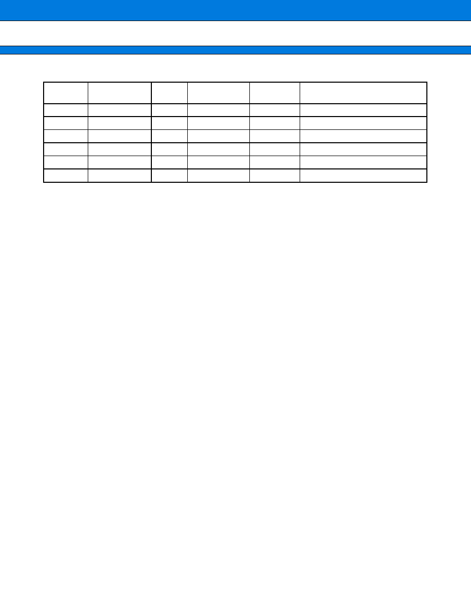
Note : If pins VDD35 (25, 51, 182, 198) are connected to 3.3 V then the external bus interface (pins 1-52, 182-208)
can be operated at 3.3 V levels.
Pin No.
Pin Name
I/O
General
Purpose IO Port
Circuit Type
Function
203
D18
I/O
Q
Ext. Bus Data Bit 18
204
D19
I/O
Q
Ext. Bus Data Bit 19
205
D20
I/O
Q
Ext. Bus Data Bit 20
206
D21
I/O
Q
Ext. Bus Data Bit 21
207
D22
I/O
Q
Ext. Bus Data Bit 22
208
D23
I/O
Q
Ext. Bus Data Bit 23
MB91360G Series
26
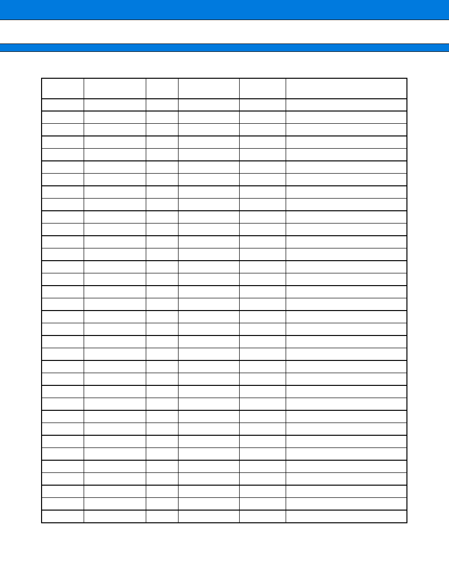
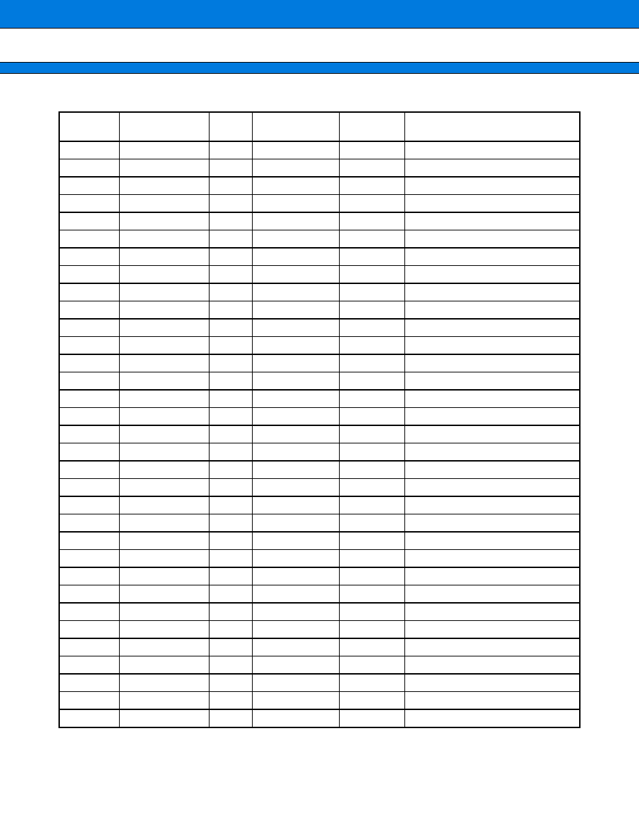
∑ MB91F369GA I/O Pins and Their Functions
(Continued)
Pin No.
Pin Name
I/O
General
Purpose IO Port
Circuit Type
Function
1
A4
I/O
Q
Ext. Bus Address Bit 4
2
A5
I/O
Q
Ext. Bus Address Bit 5
3
A6
I/O
Q
Ext. Bus Address Bit 6
4
A7
I/O
Q
Ext. Bus Address Bit 7
5
A8
I/O
Q
Ext. Bus Address Bit 8
6
A9
I/O
Q
Ext. Bus Address Bit 9
7
A10
I/O
Q
Ext. Bus Address Bit 10
8
A11
I/O
Q
Ext. Bus Address Bit 11
9
VDD35
separated Ext. Bus VDD, 3.3 or 5.0 V
10
CLK
I/O
A
Ext. Bus Clock
11
VSS
12
A12
I/O
Q
Ext. Bus Address Bit 12
13
A13
I/O
Q
Ext. Bus Address Bit 13
14
A14
I/O
Q
Ext. Bus Address Bit 14
15
A15
I/O
Q
Ext. Bus Address Bit 15
16
A16
I/O
Q
Ext. Bus Address Bit 16
17
A17
I/O
Q
Ext. Bus Address Bit 17
18
A18
I/O
Q
Ext. Bus Address Bit 18
19
A19
I/O
Q
Ext. Bus Address Bit 19
20
A20
I/O
Q
Ext. Bus Address Bit 20
21
VDD35
separated Ext. Bus VDD, 3.3 or 5.0 V
22
VSS
23
CS4X
I/O
P74
A
Chip Select 4
24
CS5X
I/O
P75
A
Chip Select 5
25
CS6X
I/O
P76
A
Chip Select 6
26
RDX
I/O
S
Ext. Bus Control
27
BGRNTX
I/O
P81
A
Ext. Bus Control
28
BRQ
I/O
P82
A
Ext. Bus Control
29
AS
I/O
P90
A
Ext. Bus Control
30
ALE
I/O
P91
A
Ext. Bus Control
31
AH
I/O
P93
A
Ext. Bus Control Signal
32
CS0X
I/O
P94
A
Chip select 0
33
CS1X
I/O
P95
A
Chip select 1
MB91360G Series
27
(Continued)
Pin No.
Pin Name
I/O
General
Purpose IO Port
Circuit Type
Function
34
CS2X
I/O
P96
A
Chip select 2
35
CS3X
I/O
P97
A
Chip select 3
36
DREQ0
I/O
PB0
A
DMA Request 0
37
DACK0
I/O
PB1
A
DMA Acknowledge 0
38
DEOP0
I/O
PB2
A
DMA EOP 0
39
VSS
40
VDD35
separated Ext. Bus VDD, 3.3 or 5.0 V
41
AVRH
R
Analog Reference High
42
AVCC
Analog VCC
43
AVSS, AVRL
Analog VSS, Analog Reference Low
44
AN0
I/O
PH0
B
ADC Input 0
45
AN1
I/O
PH1
B
ADC Input 1
46
AN2
I/O
PH2
B
ADC Input 2
47
AN3
I/O
PH3
B
ADC Input 3
48
AN4
I/O
PH4
B
ADC Input 4
49
AN5
I/O
PH5
B
ADC Input 5
50
AN6
I/O
PH6
B
ADC Input 6
51
AN7
I/O
PH7
B
ADC Input 7
52
AN8
I/O
PG0
B
ADC Input 8
53
AN9
I/O
PG1
B
ADC Input 9
54
ALARM
I
D
Alarm Comparator Input
55
VSS
56
VDD
57
ATGX
I/O
P13
A
ADC Trigger Input
58
MD0
I
T
Mode Pin 0
59
MD1
I
T
Mode Pin 1
60
MD2
I
T
Mode Pin 2
61
HSTX
I
E
Hardware Standby
62
INITX
I
U
Initual Pin
63
TESTX
I
E
Test Input
(should be connected to VDD)
64
CPUTESTX
I
E
Test Input
(should be connected to VDD)
65
LTESTX
I
E
Test Input
(should be connected to VDD)
66
VDD

MB91360G Series
28
(Continued)
Pin No.
Pin Name
I/O
General
Purpose IO Port
Circuit Type
Function
67
VSS
68
INT0
I/O
PK0
A
Ext. Interrupt 0
69
INT1
I/O
PK1
A
Ext. Interrupt 1
70
INT2
I/O
PK2
A
Ext. Interrupt 2
71
INT3
I/O
PK3
A
Ext. Interrupt 3
72
INT4
I/O
PK4
A
Ext. Interrupt 4
73
INT5
I/O
PK5
A
Ext. Interrupt 5
74
INT6
I/O
PK6
A
Ext. Interrupt 6
75
INT7
I/O
PK7
A
Ext. Interrupt 7
76
SGO
I/O
PM0
A
Sound Generator SGO
77
SGA
I/O
PM1
A
Sound Generator SGA
78
SDA
I/O
PM2
Y
I
2
C SDA
79
SCL
I/O
PM3
Y
I
2
C SCL
80
SOT4
I/O
PN0
A
SIO Output
81
SIN4
I/O
PN1
A
SIO Input
82
SCK4
I/O
PN2
A
SIO Clock
83
SIN3
I/O
PN3
A
SIO Input
84
SOT3
I/O
PN4
A
SIO Output
85
SCK3
I/O
PN5
A
SIO Clock
86
VSS
87
VDDI
Supply voltage for internal regulator
88
VDDI
Supply voltage for internal regulator
89
VDDI
Supply voltage for internal regulator
90
VDDI
Supply voltage for internal regulator
91
VCC3C
Capacitor pin for internal regulator
92
VSS
93
TX0
I/O
PP0
Q
CAN 0 TX
94
RX0
I/O
PP1
Q
CAN 0 RX
95
TX1
I/O
PP2
Q
CAN 1 TX
96
RX1
I/O
PP3
Q
CAN 1 RX
97
SIN0
I/O
PQ0
A
UART 0 Input
98
SOT0
I/O
PQ1
A
UART 0 Output
99
VDD
100
VSS
MB91360G Series
29
(Continued)
Pin No.
Pin Name
I/O
General
Purpose IO Port
Circuit Type
Function
101
OCPA0
I/O
PO0
A
PPG Output
102
OCPA1
I/O
PO1
A
PPG Output
103
OCPA2
I/O
PO2
A
PPG Output
104
OCPA3
I/O
PO3
A
PPG Output
105
VDDX
106
X0
H
4 MHz Oscillator Pin
107
X1
H
4 MHz Oscillator Pin
108
VSS
109
VDD
110
MONCLK
O
Q1
System Clock Output
111
VSS
112
VDD35
separated Ext. Bus VDD, 3.3 or 5.0 V
113
VSS
114
WR3X
I/O
S
Ext. Bus Control
115
WR2X
I/O
S
Ext. Bus Control
116
WR1X
I/O
S
Ext. Bus Control
117
WR0X
I/O
S
Ext. Bus Control
118
RDY
I/O
S
Ext. Bus Control
119
VDD35
separated Ext. Bus VDD, 3.3 or 5.0 V
120
VSS
121
D0
I/O
Q
Ext. Bus Data Bit 0
122
D1
I/O
Q
Ext. Bus Data Bit 1
123
D2
I/O
Q
Ext. Bus Data Bit 2
124
D3
I/O
Q
Ext. Bus Data Bit 3
125
D4
I/O
Q
Ext. Bus Data Bit 4
126
D5
I/O
Q
Ext. Bus Data Bit 5
127
D6
I/O
Q
Ext. Bus Data Bit 6
128
D7
I/O
Q
Ext. Bus Data Bit 7
129
D8
I/O
Q
Ext. Bus Data Bit 8
130
D9
I/O
Q
Ext. Bus Data Bit 9
131
D10
I/O
Q
Ext. Bus Data Bit 10
132
D11
I/O
Q
Ext. Bus Data Bit 11
133
D12
I/O
Q
Ext. Bus Data Bit 12
134
D13
I/O
Q
Ext. Bus Data Bit 13
MB91360G Series
30
(Continued)
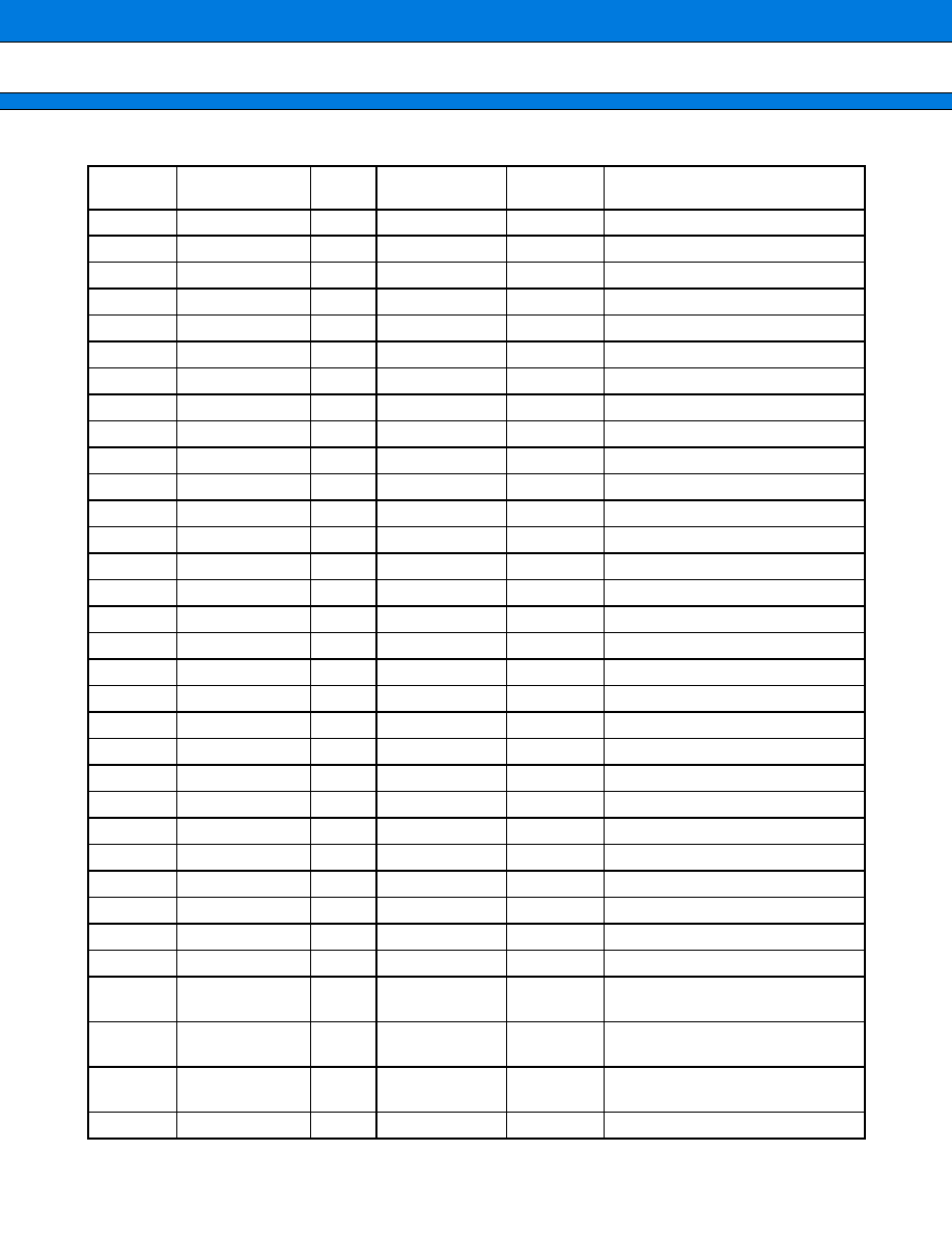
Note : If pins VDD35 (9, 21, 40, 112, 119, 137, 155) are connected to a 3.3 V supply the external bus interface (pins
1-40, 112-160) can be operated at 3.3 V levels.
Pin No.
Pin Name
I/O
General
Purpose IO Port
Circuit Type
Function
135
D14
I/O
Q
Ext. Bus Data Bit 14
136
D15
I/O
Q
Ext. Bus Data Bit 15
137
VDD35
separated Ext. Bus VDD, 3.3 or 5.0 V
138
VSS
139
D16
I/O
Q
Ext. Bus Data Bit 16
140
D17
I/O
Q
Ext. Bus Data Bit 17
141
D18
I/O
Q
Ext. Bus Data Bit 18
142
D19
I/O
Q
Ext. Bus Data Bit 19
143
D20
I/O
Q
Ext. Bus Data Bit 20
144
D21
I/O
Q
Ext. Bus Data Bit 21
145
D22
I/O
Q
Ext. Bus Data Bit 22
146
D23
I/O
Q
Ext. Bus Data Bit 23
147
D24
I/O
Q
Ext. Bus Data Bit 24
148
D25
I/O
Q
Ext. Bus Data Bit 25
149
D26
I/O
Q
Ext. Bus Data Bit 26
150
D27
I/O
Q
Ext. Bus Data Bit 27
151
D28
I/O
Q
Ext. Bus Data Bit 28
152
D29
I/O
Q
Ext. Bus Data Bit 29
153
D30
I/O
Q
Ext. Bus Data Bit 30
154
D31
I/O
Q
Ext. Bus Data Bit 31
155
VDD35
separated Ext. Bus VDD, 3.3 or 5.0 V
156
VSS
157
A0
I/O
Q
Ext. Bus Address Bit 0
158
A1
I/O
Q
Ext. Bus Address Bit 1
159
A2
I/O
Q
Ext. Bus Address Bit 2
160
A3
I/O
Q
Ext. Bus Address Bit 3
MB91360G Series
31
s
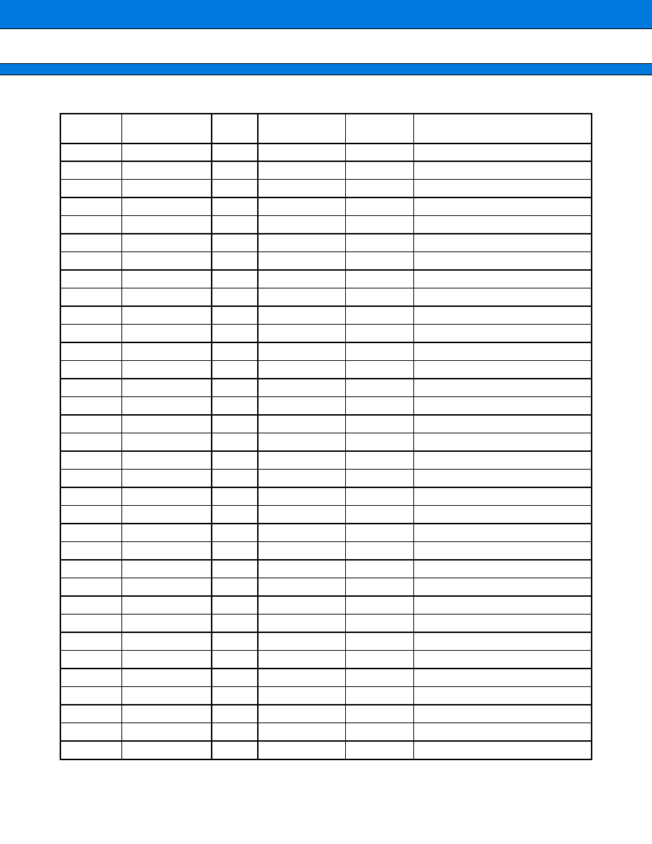
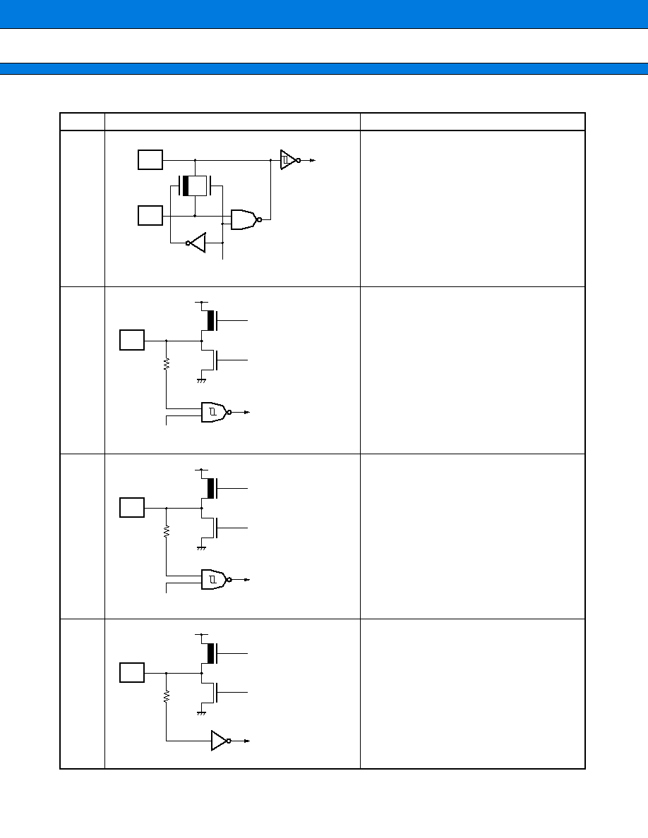
I/O CIRCUIT TYPE
(Continued)
Type
Circuit type
Remarks
A
∑ I/O,
CMOS Automotive Schmitt-Trigger Input,
STOP control,
I
OH
=
4 mA, I
OL
=
4 mA
B
∑ I/O,
CMOS Automotive Schmitt-Trigger Input,
Analog Input,
STOP control,
I
OH
=
4 mA, I
OL
=
4 mA
C
∑ Analog output
D
∑ Analog Input
P
N
R
Stop control
Digital input
Digital output
Digital output
V
SS
P
N
R
R
Stop control
Digital input
Analog input
Digital output
Digital output
V
SS
P
N
Analog output
V
SS
V
CC
P
N
R
Analog input
V
SS
V
CC
MB91360G Series
32
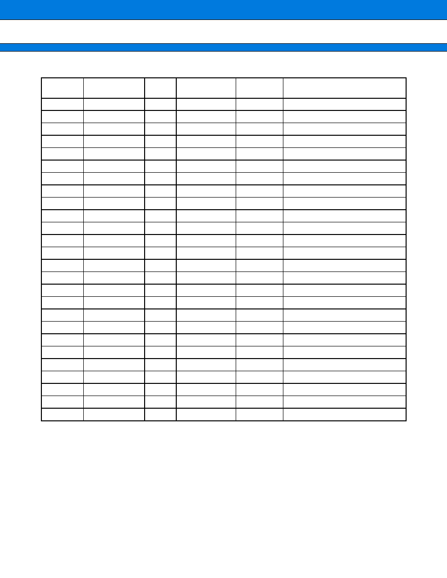
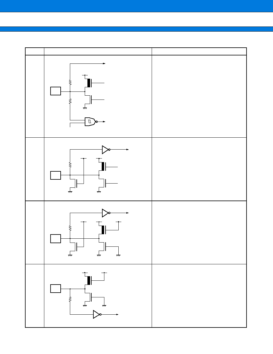
(Continued)
Type
Circuit type
Remarks
E
∑ CMOS Schmitt-Trigger Input,
Pullup Resistor: 50 k
F
∑ CMOS Schmitt-Trigger Input
G
∑ Tristate Output,
I
OH
=
4 mA, I
OL
=
4 mA
H
∑ 4 MHz Oscillator Pin
P
N
R
Digital input
P
V
SS
V
SS
V
CC
V
CC
P
N
R
Digital input
V
SS
V
CC
P
N
Digital output
Digital output
V
SS
V
CC
Stop control
Clock input
X1
X0
MB91360G Series
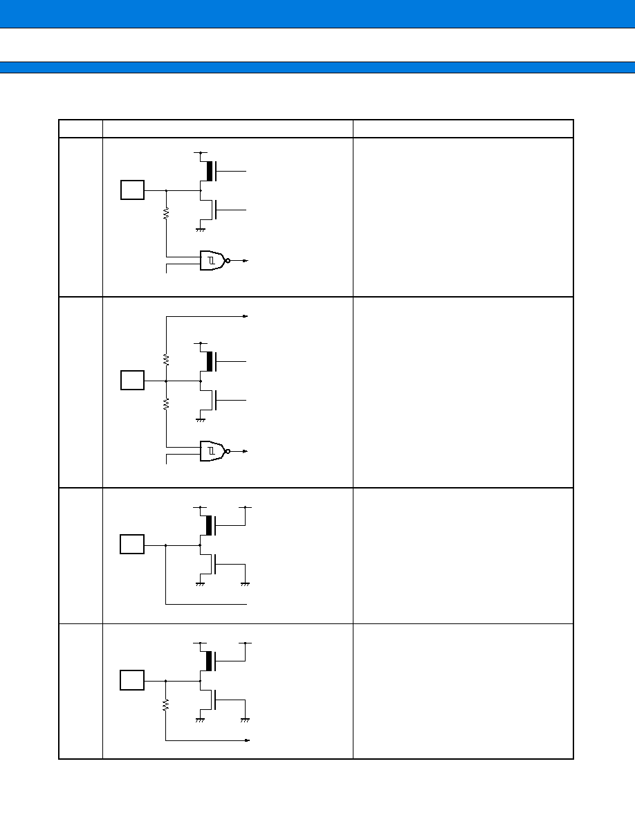
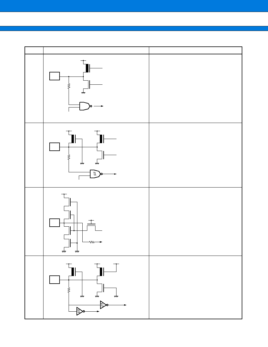
33
(Continued)
Type
Circuit type
Remarks
I
∑ 32 kHz Oscillator Pin
J
∑ I/O,
CMOS Automotive Schmitt-Trigger Input,
STOP control (LED) ,
I
OH
=
14 mA, I
OL
=
24 mA
K
∑ I/O,
CMOS Automotive Schmitt-Trigger Input,
STOP control (SMC) ,
I
OH
=
30 mA, I
OL
=
30 mA
∑ Typ slew rate of 40 ns
L
∑ I/O,
CMOS Input: 5 V or 3 V input,
I
OH
=
4 mA, I
OL
=
4 mA
Stop control
Clock input
X1A
X0A
P
N
R
Stop control
Digital input
Digital output
Digital output
V
SS
P
N
R
Stop control
Digital input
Digital output
Digital output
V
SS
P
N
R
Digital input
Digital output
Digital output
V
SS
V
CC
MB91360G Series
34
(Continued)
Type
Circuit type
Remarks
M
∑ I/O,
CMOS Automotive Schmitt-Trigger Input,
Analog Input, STOP control (SMC) ,
I
OH
=
30 mA, I
OL
=
30 mA
∑ Typ slew rate of 40 ns
N
∑ I/O,
CMOS Input,
Pulldown Resistor: 50 k
,
5 V or 3 V input,
I
OH
=
4 mA, I
OL
=
4 mA
O
∑ CMOS Input,
Pulldown Resistor: 50 k
,
5 V or 3 V input
P
∑ CMOS Input: 3 V input
P
N
R
R
Stop control
Digital input
Analog input
Digital output
Digital output
V
SS
P
N
R
Digital input
Digital output
Digital output
N
V
SS
V
CC
P
N
R
Digital input
N
V
SS
V
SS
V
CC
V
CC
P
N
R
Digital input
V
SS
V
CC
MB91360G Series
35
(Continued)
Type
Circuit type
Remarks
Q/Q1
∑ Q : I/O CMOS Input,
STOP control,
I
OH
=
4 mA, I
OL
=
4 mA
∑ Q1 : I/O CMOS Input,
STOP control,
I
OH
=
8 mA, I
OL
=
8 mA
S
∑ I/O,
CMOS Schmitt-Trigger Input,
STOP control,
Pullup Resistor : 10 k
,
I
OH
=
4 mA, I
OL
=
4 mA
T
∑ CMOS Input
∑ can withstand high V
ID
for flash
programming
U
∑ CMOS Schmitt-Trigger Input,
Pullup Resistor: 50 k
,
3 V and 5 V input to the core
P
N
R
Stop control
Digital input
Digital output
Digital output
V
SS
P
N
R
P
V
SS
V
CC
Digital output
Digital output
Digital input
Stop control
R
Control signal
MD Input
P
N
R
Digital input
P
V
SS
V
SS
V
CC
V
CC
MB91360G Series
36
(Continued)
Note : Symbols used in circuit types (Common to all circuit diagrams)
P : P channel transistor
N : N channel transistor
R : Diffusion resistor
Type
Circuit type
Remarks
V
∑ I/O,
CMOS Schmitt-Trigger Input,
STOP control,
Pullup Resistor: 50 k
,,
I
OH
=
4 mA, I
OL
=
4 mA
W
∑ I/O,
CMOS Input: 3 V input
X
∑ Tristate Output, 3 V
Y
∑ I/O CMOS Input,
STOP control,
I
OH
=
3 mA, I
OL
=
3 mA,
in I
2
C mode operating as open drain
outputs
P
N
R
P
V
SS
V
CC
Digital output
Digital output
Digital input
Stop control
P
N
R
Digital input
Digital output
Digital output
V
SS
3 V
P
N
Digital output
Digital output
V
SS
3 V
P
N
R
Stop control
Digital input
Digital output
Digital output
V
SS

MB91360G Series
37
Circuit
Type
Description
A
I/O, I
OH
=
4 mA
/
I
OL
=
4 mA, CMOS Automotive Schmitt-Trigger Input, STOP control
B
I/O, I
OH
=
4 mA
/
I
OL
=
4 mA, CMOS Automotive Schmitt-Trigger Input, Analog Input, STOP control
C
Analog Output
D
Analog Input
E
CMOS Schmitt-Trigger Input, Pull-up Resistor: 50 k
,
F
CMOS Schmitt-Trigger Input
G
Tristate Output, I
OH
=
4 mA
/
I
OL
=
4 mA
H
4 MHz Oscillator Pin
I
32 kHz Oscillator pin
J
I/O, I
OH
=
14 mA
/
I
OL
=
24 mA, CMOS Automotive Schmitt-Trigger Input, STOP control (LED)
K
I/O, I
OH
=
30 mA
/
I
OL
=
30 mA, CMOS Automotive Schmitt-Trigger Input, STOP control, slew rate
improved for EMC (SMC)
L
I/O, I
OH
=
4 mA
/
I
OL
=
4 mA, CMOS Input: 5 V or 3 V input
M
I/O, I
OH
=
30 mA
/
I
OL
=
30 mA, CMOS Automotive Schmitt-Trigger Input, Analog Input, STOP control,
slew rate improved for EMC (SMC)
N
I/O, I
OH
=
4 mA
/
I
OL
=
4 mA, CMOS Input : 5 V or 3 V input, Pulldown Resistor: 50 k
O
CMOS Input : 5 V or 3 V input, Pulldown Resistor: 50 k
P
CMOS Input: 3 V input
Q
I/O, I
OH
=
4 mA
/
I
OL
=
4 mA, CMOS Input, STOP control
Q1
I/O, I
OH
=
8 mA
/
I
OL
=
8 mA, CMOS Input, STOP control
R
AVRL
/
AVRH Input
S
I/O, I
OH
=
4 mA
/
I
OL
=
4 mA, CMOS Input, STOP control, Pull-up Resistor: 10 k
,
T
CMOS Input, can withstand V
ID
for flash programming
U
CMOS Schmitt-Trigger Input, Pull-up Resistor: 50 k
, 3.3 V and 5 V inputs to core
W
I/O, I
OH
=
4 mA
/
I
OL
=
4 mA, CMOS Input: 3 V input
X
Tristate Output, I
OH
=
4 mA
/
I
OL
=
4 mA, 3 V
Y
I/O, I
OH
=
3 mA
/
I
OL
=
3 mA (I
2
C) , CMOS Input, STOP control
MB91360G Series
38
s
HANDLING DEVICES
1.
Preventing latch-up
Latch-up may occur in a CMOS IC if a voltage greater than V
DD
or less than V
SS
is applied to an input or output
pin or if the voltage applied between V
DD
and V
SS
exceeds the rating. If latch-up occurs, the power supply current
increases rapidly resulting in thermal damage to circuit elements. Therefore, ensure that maximum ratings are
not exceeded in circuit operation.
2.
Connecting unused pins
Leaving unused input pins open may result in misbehavior or latch up and possible permanent damage of the
device. Therefore they must be tied to V
DD
or V
SS
through resistors. In this case those resistors should be more
than 2 KOhm.
Unused bidirectional pins should be set to the output state and can be left open, or the input state with the above
described connection.
The resistor of more than 2 KOhm is used to limit currents through the protection diodes. In case of voltages at
the not used pin of 0.3 V or more below V
SS
or 0.3 V or more above V
DD
currents which could cause latch-up will
flow through those diodes.
3.
External reset input
When inputting an "L" level to the INITX pin, hold this low level at the INITX pin long enough so that after release
of the low level at INITX and the passing of the built in waiting time stable oscillation of the oscillation circuit is
achieved. INITX must be pulled low for at least 8 cycles of the 4 MHz oscillation clock.
4.
Power supply pins
All V
DD
pins should be connected to the same potential (exception can be the external bus interface on F362GA
and F369GA) . The analogue supply voltage (AV
CC
) must not be turned on before the digital supply voltage. If
the external bus interface is supplied with 3.3 V this voltage also must not be turned on before the 5 V digital
voltage has been switched on. If the supply voltage to the external bus interface is switched off (it may not be
tristate but should be pulled low) it must be made sure that all related signals do not have a voltage higher than
this pulled down supply.
When multiple V
DD
and V
SS
pins are provided, be sure to connect all V
DD
and V
SS
pins to the power supply or
ground externally. Although pins at the same potential are connected together in the internal device design so
as to prevent malfunctions such as latch-up, connecting all V
DD
and V
SS
pins appropriately minimizes unwanted
radiation, prevents malfunction of strobe signals due to increases in the ground level, and keeps the overall
output current rating.
Also, take care to connect V
DD
and V
SS
to current source in the lowest possible impedance.
Connection of a ceramic bypass capacitor of approximately 0.1
µ
F between V
DD
and V
SS
close to the device is
recommended.
The MB91360G series contains a regulator. To use the device with the 5-V power supply, supply 5-V power to
the V
CC
pins and be sure to connect a bypass capacitor of 10
µ
F parallel to 10 nF to the V
CC
3C pin for the regulator.
5 V
5 V
10
µ
F
10 nF
V
CC
3C
V
CC
AV
CC
AVRH
AV
SS
V
SS
GND
[Use with 5-V power supply]

MB91360G Series
39
5.
Crystal oscillator circuit
Noise in the vicinity of the X0 and X1 pins can be a cause of device malfunction. Design the circuit board so that
X0, X1, the crystal oscillator (or ceramic oscillator) , and the bypass capacitor to ground are located as close to
the device as possible.
A printed circuit board design that surrounds the X0 and X1 pins with ground provides for stable operation and
is strongly recommended.
6.
Mode pins
Connect the mode pins (MD0 to MD2) directly to V
DD
or V
SS
.
To prevent the device unintentionally entering test mode due to noise, lay out the printed circuit board so as to
minimize the distance from the mode pins to V
DD
or V
SS
and to provide a low-impedance connection.
7.
Turning the power supply on
Immediately after power on always execute INIT at the INITX pin (start with a low level at the INITX pin) . Hold
this low level at the INITX pin long enough so that after release of the low level at INITX and the passing of the
built in waiting time stable oscillation of the oscillation circuit is achieved. INITX must be pulled low for at least
8 cycles of the 4 MHz oscillation clock.
The analogue supply voltage (AV
CC
) must not be turned on before the digital supply voltage. If the external bus
interface is supplied with 3.3 V this voltage also must not be turned on before the 5 V digital voltage has been
switched on.
8.
A state in turning power on
As long as the minimum operating voltage has not been reached during power-on the output pin levels are not
guaranteed.
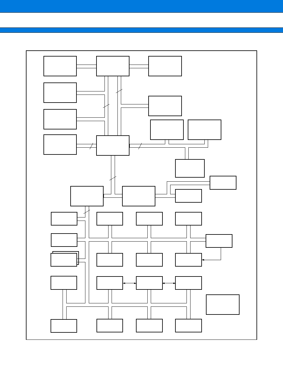
MB91360G Series
40
s
BLOCK DIAGRAM
32
32
32
16
32
32
Clock
Generation
FR50
Core
Watchdog
Timer
User RAM
D-bus
Bit Search
Module
DMA
Controller
Instruction
Cache/RAM
F-bus RAM
Bus
Converter
Boot ROM
2 KB
R-Bus
Adapter
SIO Prescaler/
SIO
U-Timer/
UART
Power Down
Reset
Subclock
Calibration
External Bus
Interface
CAN
DAC
ADC
External
Interrupt
Flash-
memory
I
2
C
Reload
Timer
ICU
LED
Sound
Generator
Alarm
Comparator
FreeRunning
Timer
Real Time
Clock
Voltage
regulator
OCU
Stepper Motor
Control
Prog. Pulse
Generator
External Bus
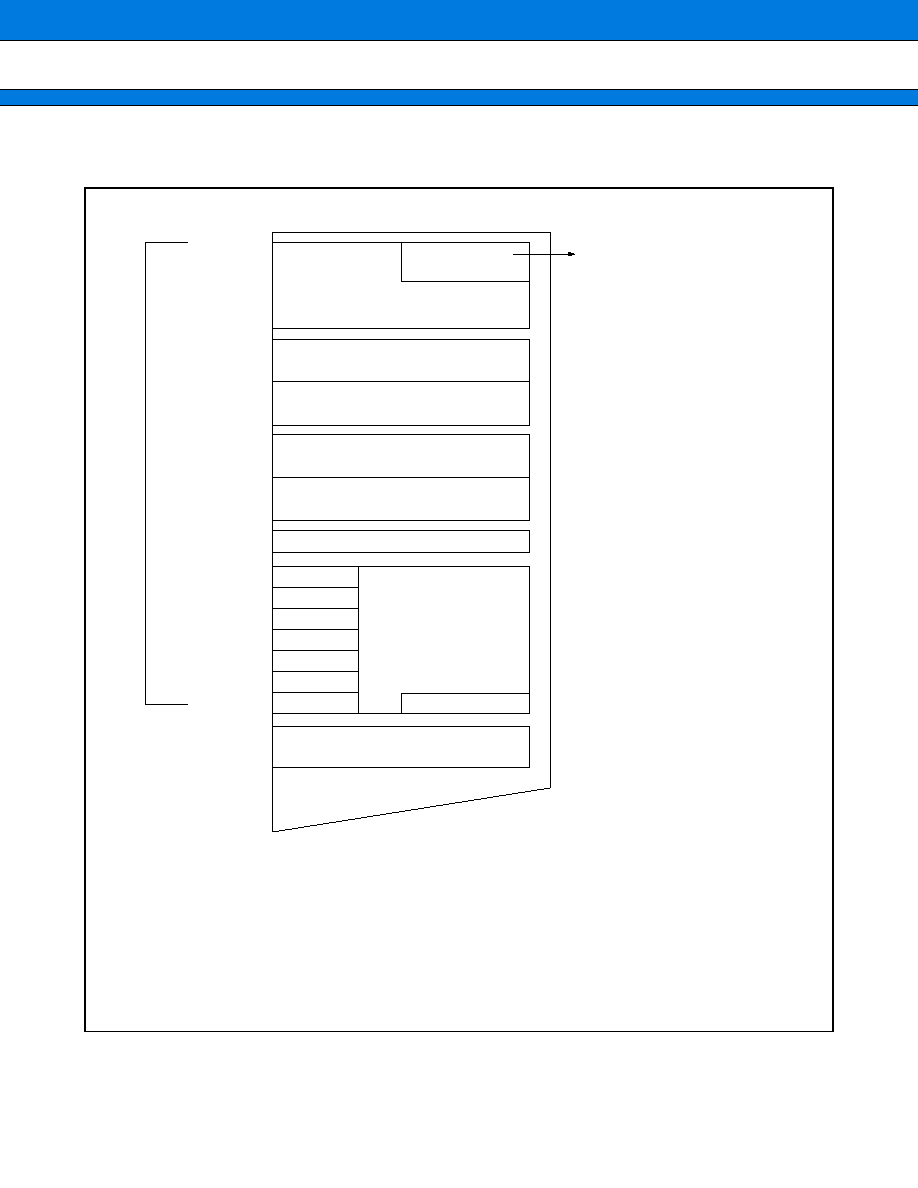
MB91360G Series
41
s
CPU CORE
1.
Memory Space
Internal memory area
00
:
0000
00
:
03FF
00
:
07FF
00
:
1000
00
:
1024
01
:
1000
01
:
1FFF
03
:
C000
03
:
FFFF
04
:
0000
04
:
3FFF
05
:
0000
05
:
07FF
08
:
0000
0F
:
4000
0F
:
FFFF
10
:
0000
128 K
128 K
128 K
64 K
16 K
16 K
32 K
CAN
Fixed Reset Vector
Bootsector
Flash Memory
on F-bus
Boot ROM
F-bus RAM
D-bus RAM
I-RAM
DMA
IO Area
Direct
Direct (short) addressing
0..0FF
:
Byte access
0..1FF
:
Halfword access (16 bit)
0..3FF
:
Word access (32 bit)
03
:
D000 - 03
:
FFFF on F362GA
04
:
0000 - 04
:
0FFF on F362GA
10
:
07FF
Addresses for CAN depend on set-
tings for the chip select areas CS7.
The addresses given here are valid
for the CS7 settings done in the Boot
ROM.
MB91360G Series
42
2.
Dedicated Registers
Each of the dedicated registers is used for a particular purpose. The dedicated registers consist of the program
counter (PC) , program status (PS) , table base register (TBR) , return pointer (RP) , system stack pointer (SS
P) , user stack pointer (USP) , and multiplication and division result registers (MDH/MDL) .
(1) Program status (PS)
PC
PS
TBR
RP
SSP
USP
MDH
MDL
XXXX XXXX
H
(Indeterminate)
XXXX XXXX
H
(Indeterminate)
XXXX XXXX
H
(Indeterminate)
XXXX XXXX
H
(Indeterminate)
XXXX XXXX
H
(Indeterminate)
0000 0000
H
000F FC00
H
32 bits
Program counter
Program status
Table base register
Return pointer
System stack pointer
User stack pointer
Multiplication and division
results resisters
Initial value
31
Bit position
20
16
ILM
SCR
CCR
10
7
8
0
CCR : Condition Code Register
SCR : System Condition Code Register
ILM : Interrupt Level Mask
MB91360G Series
43
(2) Condition Code Register (CCR)
(3) System Condition Code Register (SCR)
(4) Interrupt Level Mask Register (ILM)
(Bit)
Initial value
--00XXXX
B
7
6
5
4
3
2
1
0
S
I
N
Z
V
C
(Bit)
Initial value
XX0
B
10
9
8
D1
D0
T
(Bit)
Initial value
01111
B
20
19
18
17
16
ILM4 ILM3 ILM2 ILM1 ILM0
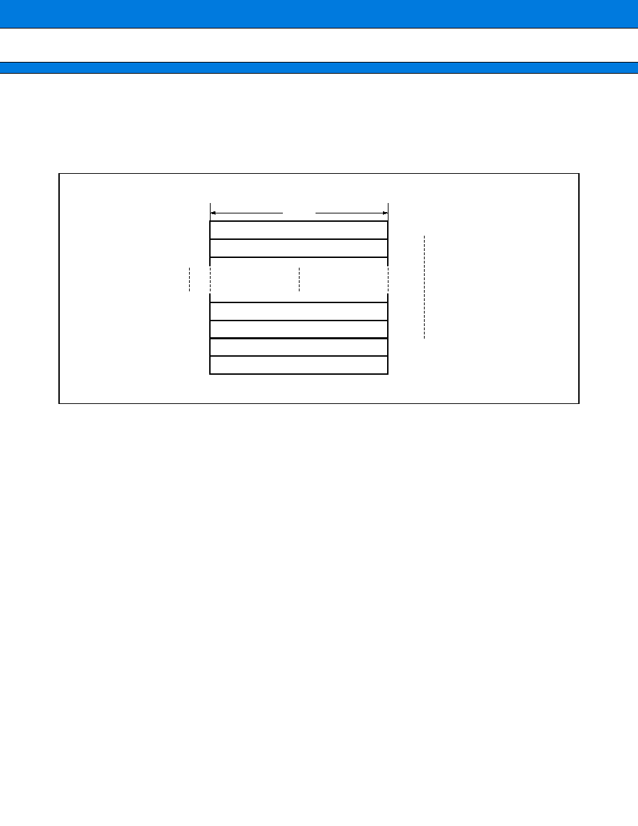
MB91360G Series
44
3.
General-Purpose Registers
The general-purpose registers are CPU registers R0 to R15. The register are used as the accumulator for
operations and as pointers (a field indicating an address) for memory access. The user can specify the purpose
for which the general-purpose registers are used.
Among 16 general-purpose registers, the following registers assume a special purpose. This enhances some
instructions.
The initial value of R0 to R14 after a reset is indeterminate. The initial value of R15 is 00000000
H
(SSP value) .
R13
: Virtual accumulator (AC)
R14
: Frame pointer (FP)
R15
: Stack pointer (SP)
R0
R1
R12
R13
R14
R15
AC (Accumulator)
FP (Frame Pointer)
SP (Stack Pointer)
XXXX XXXX
H
XXXX XXXX
H
0000 0000
H
32-bits
Initial value
Register bank structure
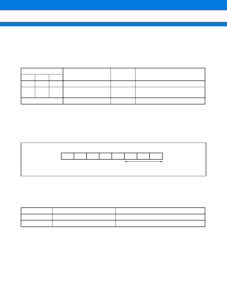
MB91360G Series
45
s
MODE SETTING
The FR50 series of devices uses mode pins (MD2 to MD0) and a mode register (MODR) to set the operation
mode.
(1) Mode Pins
Three mode pins (MD2 to MD0) are used to specify the reset mode vector access area.
(2) Mode Register (MODR)
The data to be written to 0000_7FDH using mode vector fetch is called mode data.
MODR is located at 0000_07FDH. After an operation mode has been set in MODR, the device operates in this
operation mode. MODR is set only when a reset factor (INIT level) occurs. User programs cannot write data to
MODR.
<
Mode Register (MODR)
>
[Bits 7 to 3] : (Reserved bits)
Always set 00000 at bits 7 to 3. Operation is not guaranteed when other values are set.
[Bit 2] : ROMA (internal ROM enable bit)
The ROMA bit is used to set whether to validate the internal ROM area (Fbus memory area) .
Mode Pins
Mode name
Reset vector
access area
Remarks
MD2
MD1
MD0
0
0
0
Internal ROM mode vector
Internal
0
0
1
External ROM mode vector
External
The mode register is used to set the bus
width.
remaining settings
Reserved
ROMA
Function
Remarks
0
External ROM mode
Access to the Fbus area is external.
1
Internal ROM mode
Address
Initial value
0000 07FD
H
XXXXXXXX
7
6
5
4
3
2
1
0
0
0
0
0
0
ROMA
WTH1
Operation mode setting bit
WTH0
MB91360G Series
46
[Bits 1 and 0] : WTH1 and WTH0 (bus width/single chip mode specifying bits)
The WTH1 and WTH0 bits are used to set the bus width (valid when operation mode is external bus mode) and
the single chip mode. When the operation mode is the external bus mode, this value is set at the BW1 and BW0
bits of AMD0 (CS0 area) .
(3) Fixed Vector
If MB91360 series devices are started in mode MD[2 : 0]
=
000, the internal fixed mode vector (FMV
=
0x06)
and the fixed reset vector are used. The fixed reset vector points to the start address of the internal Boot ROM.
This enables access to the F-bus area, to the internal CAN modules and the internal flash memory.
See also section Boot ROM.
WTH1
WTH0
Function
Remarks
0
0
8-bit bus width
External bus mode
0
1
16-bit bus width
External bus mode
1
0
32-bit bus width
External bus mode
1
1
Single chip mode
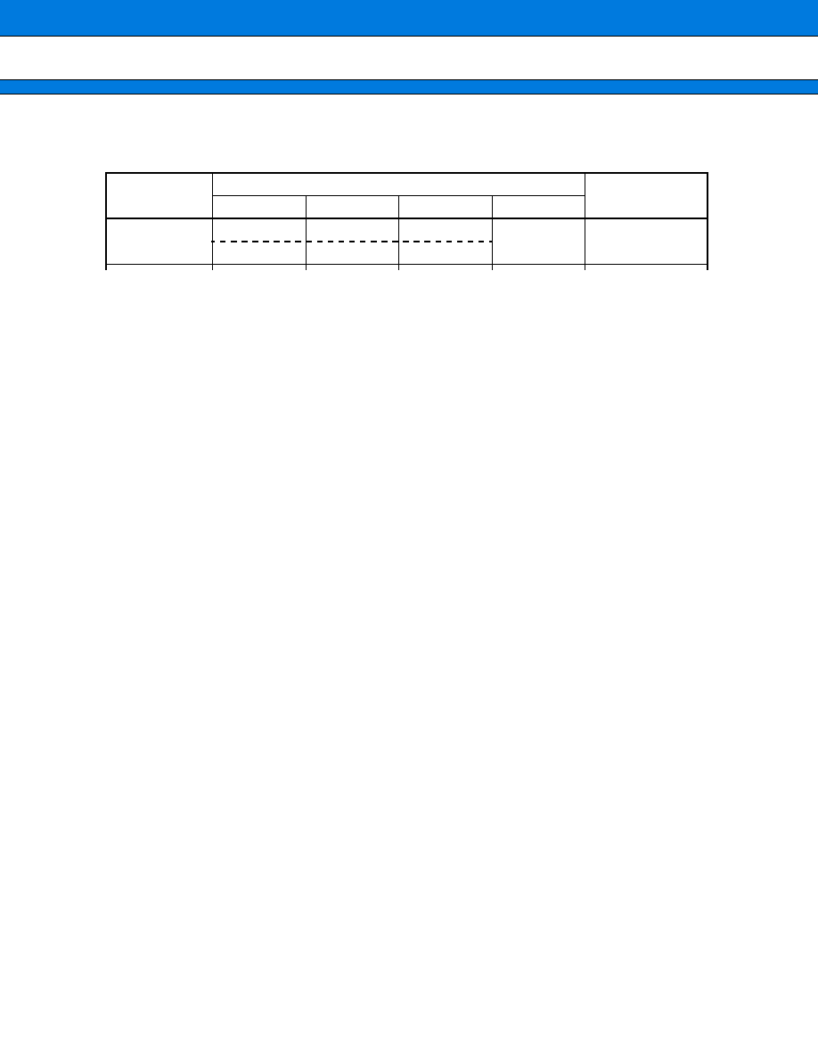
MB91360G Series
47
s
I/O MAP
∑ How to Read the I/O Map
Read/Write attribute
Register initial value after a reset (bit initial values)
"1" : initial value "1", "0" : initial value "0",
"x" : initial value "X" (indeterminate) ,
"
" indicates non-existent bits
Register name (The register in column 1 is at location 4n, the register in
column 2 at 4n
+
1, and so on.)
Location of far left of register (
+
0) .
+
1
+
2, and
+
3 each increment the loca-
tion by one. When performing word access, the register in column 1 is
placed at the MSB end of the data.
Precautions :
∑ Do not use RMW instructions on registers containing write-only (W) bits.
RMW instructions (RMW : read-modify-write)
AND Rj, @Ri OR Rj, @Ri EOR Rj, @Ri
ANDH Rj, @Ri ORH Rj, @Ri EORH Rj, @Ri
ANDB Rj, @Ri ORB Rj, @Ri EORB Rj, @Ri
BANDL #u4, @Ri BORL #u4, @Ri BEORL #u4, @Ri
BANDH #u4, @Ri BORH #u4, @Ri BEORH #u4, @Ri
∑ The data in reserved areas and areas marked "
" is indeterminate. Do not use those ares !
Address
Register
Internal
peripheral
+
+
+
+
0
+
+
+
+
1
+
+
+
+
2
+
+
+
+
3
000014
H
PDRG[R/W]
PDRH[R/W]
PDRI[R/W]
Port data register
XXXXXXXX
XXXXXXXX
- - - - XXXX
MB91360G Series
48
(Continued)
Address
Register
Block
+
+
+
+
0
+
+
+
+
1
+
+
+
+
2
+
+
+
+
3
000000
H
Reserved
Reserved
Reserved
Reserved
T-unit
Port Data
Register
000004
H
Reserved
Reserved
Reserved
PDR7 [R/W]
-111 - - - -
000008
H
PDR8 [R/W]
XXXXXXXX
PDR9 [R/W]
XXXXXXX1
PDRB [R/W]
- - - - - XXX
00000C
H
000010
H
PDRG [R/W]
XXXXXXXX
PDRH [R/W]
XXXXXXXX
PDRI [R/W]
X - - - X - - -
PDRJ [R/W]
XXXXXXXX
R-bus
Port Data
Register
000014
H
PDRK [R/W]
XXXXXXXX
PDRL [R/W]
XXXXXXXX
PDRM [R/W]
- - - - XXXX
PDRN [R/W]
- - XXXXXX
000018
H
PDRO [R/W]
XXXXXXXX
PDRP [R/W]
- - XXXXX
PDRQ [R/W]
- - XXXXX
PDRR [R/W]
XXXXXXXX
00001C
H
PDRS [R/W]
XXXXXXXX
000020
H
to
00003C
H
Reserved
000040
H
EIRR [R/W]
00000000
ENIR [R/W]
00000000
ELVR [R/W]
00000000 00000000
Ext int/NMI
000044
H
DICR [R/W]
- - - - - - - 0
HRCL [R/W, R]
0 - - 11111
CLKR2 [R/W]
- - - - - 000
reserved
DLYI/I-unit
RTC
000048
H
TMRLR0 [W]
XXXXXXXX XXXXXXXX
TMR0 [R]
XXXXXXXX XXXXXXXX
Reload Timer 0
00004C
H
TMCSR0 [R/W]
- - - - 0000 - - - 00000
000050
H
TMRLR1 [W]
XXXXXXXX XXXXXXXX
TMR1 [R]
XXXXXXXX XXXXXXXX
Reload Timer 1
000054
H
TMCSR1 [R/W]
- - - - 0000 - - - 00000
000058
H
TMRLR2 [W]
XXXXXXXX XXXXXXXX
TMR2 [R]
XXXXXXXX XXXXXXXX
Reload Timer 2
00005C
H
TMCSR2 [R/W]
- - - - 0000 - - - 00000
000060
H
SSR0 [R/W]
00001 - 00
SIDR0 [R/W]
XXXXXXXX
SCR0 [R/W, W]
00000100
SMR0 [R/W, W]
00 - - 0 - 0 -
UART0
000064
H
ULS0 [R/W]
- - - - 0000
MB91360G Series
49
(Continued)
Address
Register
Block
+
+
+
+
0
+
+
+
+
1
+
+
+
+
2
+
+
+
+
3
000068
H
UTIM0/UTIMR0 [R/W]
00000000 00000000
DRCL0 [W]
- - - - - - - -
UTIMC0 [R/W]
0 - - - 0 - 01
U-TIMER 0
00006C
H
SSR1 [R/W, R]
00001 - 00
SIDR1 [R/W]
XXXXXXXX
SCR1 [R/W, W]
00000100
SMR1 [R/W, W]
00 - - 0 - 0 -
UART1
000070
H
ULS1 [R/W]
- - - - 0000
000074
H
UTIM1/UTIMR1 [R/W]
00000000 00000000
DRCL1 [W]
- - - - - - - -
UTIMC1 [R/W]
0 - - - - - 01
U-TIMER 1
000078
H
SSR2 [R/W, R]
00001 - 00
SIDR2 [R/W]
XXXXXXXX
SCR2 [R/W, W]
00000100
SMR2 [R/W, W]
00 - - 0 - 0 -
UART2
00007C
H
ULS2 [R/W]
- - - - 0000
000080
H
UTIM2/UTIMR2 [R/W]
00000000 00000000
DRCL2 [W]
- - - - - - - -
UTIMC2 [R/W]
0 - - - 0 - 01
U-TIMER2
000084
H
SMCS0 [R/W, R]
00000010 - - - - 00-0
SES0 [R/W]
- - - - - - 00
SDR0 [R/W]
00000000
SIO 0
000088
H
SMCS1 [R/W, R]
00000010 - - - - 00 - 0
SES1 [R/W]
- - - - - - 00
SDR1 [R/W]
00000000
SIO 1
00008C
H
CDCR0 [R/W]
0 - - - 1111
Reserved
CDCR1 [R/W]
0 - - - 1111
Reserved
SIO 0/1
Prescaler
000090
H
Reserved
000094
H
IBCR [R/W]
00000000
IBSR [R]
00000000
IADR [R/W]
-XXXXXXX
ICCR [R/W]
- - 0XXXXX
I
2
C (old)
new I
2
C
from addr 0x184
000098
H
IDAR [R/W]
XXXXXXXX
IDBL [R/W]
- - - - - - - 0
00009C
H
ADMD [R/W, W]
- - - X0000
ADCH [R/W]
00000000
ADCS [R/W, W]
0000 - - 00
A/D Converter
0000A0
H
ADCD [R/W]
000000XX XXXXXXXX
ADBL [R/W]
- - - - - - - 0
0000A4
H
DACR [R/W]
- - - - - 000
DADR0 [R/W]
- - - - - - XX XXXXXXXX
DAC
0000A8
H
DADR1 [R/W]
- - - - - - XX XXXXXXXX
DDBL [R/W]
- - - - - - - 0
0000AC
H
IOTDBL0 [R/W]
- - - - - 000
ICS01 [R/W]
00000000
IOTDBL1 [R/W]
- - - - - 000
ICS23 [R/W]
00000000
Input Capture
0, 1, 2, 3
0000B0
H
IPCP0 [R]
XXXXXXXX XXXXXXXX
IPCP1 [R]
XXXXXXXX XXXXXXXX
0000B4
H
IPCP2 [R]
XXXXXXXX XXXXXXXX
IPCP3 [R]
XXXXXXXX XXXXXXXX
MB91360G Series
50
(Continued)
Address
Register
Block
+
+
+
+
0
+
+
+
+
1
+
+
+
+
2
+
+
+
+
3
0000B8
H
OCS01 [R/W]
- - - 0 - - 00 0000 - - 00
reserved
Output Compare
0, 1, 2.3
0000BC
H
OCCP0 [R/W]
XXXXXXXX XXXXXXXX
OCCP1 [R/W]
XXXXXXXX XXXXXXXX
0000C0
H
OCCP2 [R/W]
XXXXXXXX XXXXXXXX
OCCP3 [R/W]
XXXXXXXX XXXXXXXX
0000C4
H
Reserved
0000C8
H
TCDT0 [R/W]
XXXXXXXX XXXXXXXX
TCCS0 [R/W]
- 0000000
Free Running
Counter 0 for
ICU/OCU
0000CC
H
TCDT1 [R/W]
XXXXXXXX XXXXXXXX
TCCS1 [R/W]
- 0000000
Free Running
Counter 1 for
ICU/OCU
0000D0
H
ZPD0 [R/W]
00000010
PWC0 [R/W]
- - 000 - - 0
ZPD1 [R/W]
00000010
PWC1 [R/W]
00000 - - 0
SMC 0, 1
0000D4
H
ZPD2 [R/W]
00000010
PWC2 [R/W]
- - 000 - - 0
ZPD3 [R/W]
00000010
PWC3 [R/W]
00000 - - 0
SMC 2, 3
0000D8
H
PWC20 [R/W]
XXXXXXXX
PWC10 [R/W]
XXXXXXXX
PWS20 [R/W]
- 0000000
PWS10 [R/W]
- - 000000
SMC 0
0000DC
H
PWC21 [R/W]
XXXXXXXX
PWC11 [R/W]
XXXXXXXX
PWS21 [R/W]
- 0000000
PWS11 [R/W]
- - 000000
SMC 1
0000E0
H
PWC22 [R/W]
XXXXXXXX
PWC12 [R/W]
XXXXXXXX
PWS22 [R/W]
- 0000000
PWS12 [R/W]
- - 000000
SMC 2
0000E4
H
PWC23 [R/W]
XXXXXXXX
PWC13 [R/W]
XXXXXXXX
PWS23 [R/W]
- 0000000
PWS13 [R/W]
- - 000000
SMC 3
0000E8
H
SMDBL0 [R/W]
- - - - - - - 0
SMDBL1 [R/W]
- - - - - - 0
SMDBL2 [R/W]
- - - - - - - 0
SMDBL3 [R/W]
- - - - - - - 0
SMC 0, 1, 2, 3
0000EC
H
SGDBL [R/W]
- - - - - - - 0
SGCR [R/W, R]
0 - - - - - 00 000 - - 000
Sound
generator
0000F0
H
SGAR [R/W]
00000000
SGFR [R/W]
XXXXXXXX
SGTR [R/W]
XXXXXXXX
SGDR [R/W]
XXXXXXXX
0000F4
H
WTDBL [R/W]
- - - - - - - 0
WTCR [R/W, R]
00000000 000 - 0000
Real Time Clock
(WatchTimer)
0000F8
H
WTBR [R/W]
- - XXXXXX XXXXXXXX XXXXXXXX
0000FC
H
WTHR [R/W]
- - - 00000
WTMR [R/W]
- - 000000
WTSR [R/W]
- - 000000
000100
H
TMRLR3 [W]
XXXXXXXX XXXXXXXX
TMR3 [R]
XXXXXXXX XXXXXXXX
Reload Timer 3
000104
H
TMCSR3 [R/W]
- - - - XX - - - - - XXXXX
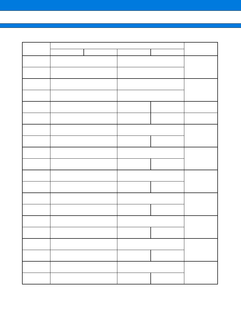
MB91360G Series
51
(Continued)
Address
Register
Block
+
+
+
+
0
+
+
+
+
1
+
+
+
+
2
+
+
+
+
3
000108
H
TMRLR4 [W]
XXXXXXXX XXXXXXXX
TMR4 [R]
XXXXXXXX XXXXXXXX
Reload Timer 4
00010C
H
TMCSR4 [R/W]
- - - - XX - - - - - XXXXX
000110
H
TMRLR5 [W]
XXXXXXXX XXXXXXXX
TMR5 [R]
XXXXXXXX XXXXXXXX
Reload Timer 5
000114
H
TMCSR5 [R/W]
- - - - XX - - - - - XXXXX
000118
H
GCN10 [R/W]
00110010 00010000
PDBL0 [R/W]
- - - 00000
GCN20 [R/W]
- - - - 0000
PWM Control 0
00011C
H
GCN11 [R/W]
00110010 00010000
PDBL1 [R/W]
- - - 00000
GCN21 [R/W]
- - - - 0000
PWM Control 1
000120
H
PTMR0 [R]
11111111 11111111
PCSR0 [W]
XXXXXXXX XXXXXXXX
PWM0
000124
H
PDUT0 [W]
XXXXXXXX XXXXXXXX
PCNH0 [R/W]
0000000 -
PCNL0 [R/W]
000000 - 0
000128
H
PTMR1 [R]
11111111 11111111
PCSR1 [W]
XXXXXXXX XXXXXXXX
PWM1
00012C
H
PDUT1 [W]
XXXXXXXX XXXXXXXX
PCNH1 [R/W]
0000000 -
PCNL1 [R/W]
000000 - 0
000130
H
PTMR2 [R]
11111111 11111111
PCSR2 [W]
XXXXXXXX XXXXXXXX
PWM2
000134
H
PDUT2 [W]
XXXXXXXX XXXXXXXX
PCNH2 [R/W]
0000000 -
PCNL2 [R/W]
000000 - 0
000138
H
PTMR3 [R]
11111111 11111111
PCSR3 [W]
XXXXXXXX XXXXXXXX
PWM3
00013C
H
PDUT3 [W]
XXXXXXXX XXXXXXXX
PCNH3 [R/W]
0000000 -
PCNL3 [R/W]
000000 - 0
000140
H
PTMR4 [R]
11111111 11111111
PCSR4 [W]
XXXXXXXX XXXXXXXX
PWM4
000144
H
PDUT4 [W]
XXXXXXXX XXXXXXXX
PCNH4 [R/W]
0000000 -
PCNL4 [R/W]
000000 - 0
000148
H
PTMR5 [R]
11111111 11111111
PCSR5 [W]
XXXXXXXX XXXXXXXX
PWM5
00014C
H
PDUT5 [W]
XXXXXXXX XXXXXXXX
PCNH5 [R/W]
0000000 -
PCNL5 [R/W]
000000 - 0
000150
H
PTMR6 [R]
11111111 11111111
PCSR6 [W]
XXXXXXXX XXXXXXXX
PWM6
000154
H
PDUT 6 [W]
XXXXXXXX XXXXXXXX
PCNH6 [R/W]
0000000 -
PCNL6 [R/W]
000000 - 0
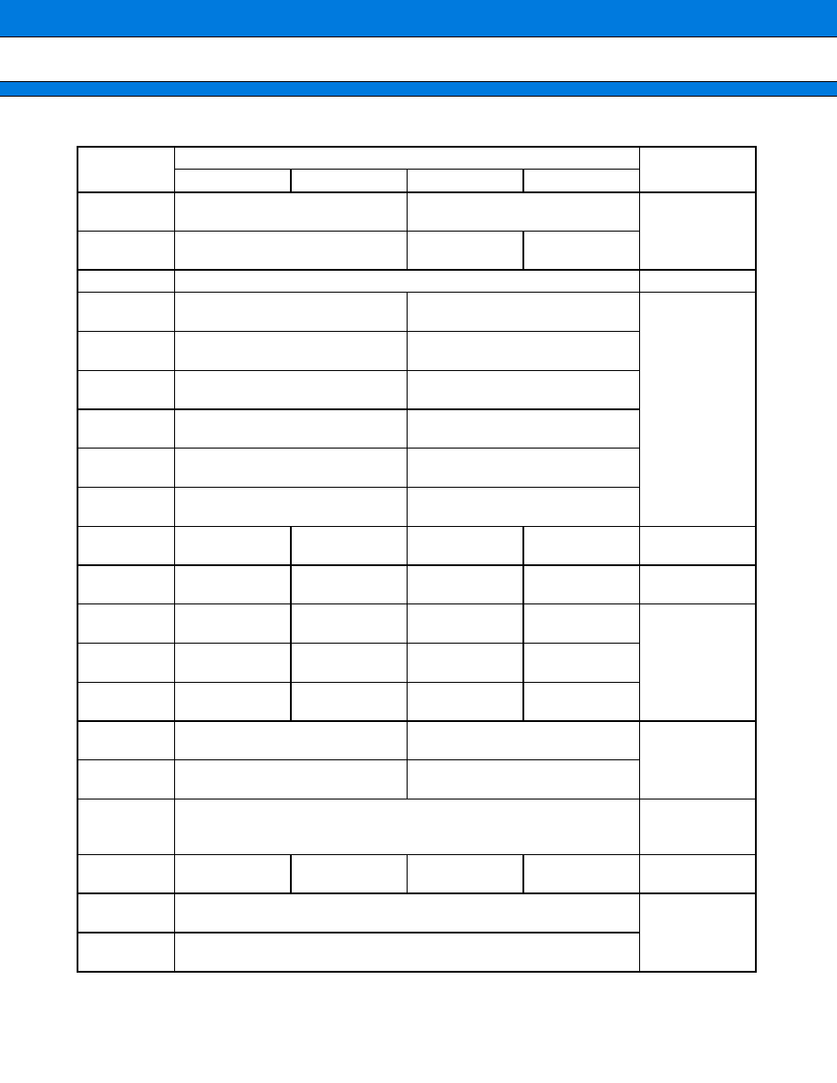
MB91360G Series
52
* : Old and new I
2
C share this bit.
(Continued)
Address
Register
Block
+
+
+
+
0
+
+
+
+
1
+
+
+
+
2
+
+
+
+
3
000158
H
PTMR7 [R]
11111111 11111111
PCSR7 [W]
XXXXXXXX XXXXXXXX
PWM7
00015C
H
PDUT7 [W]
XXXXXXXX XXXXXXXX
PCNH7 [R/W]
0000000 -
PCNL7 [R/W]
000000 - 0
000160
H
Reserved
000164
H
CMCR [R/W]
11111111 0000000
CMPR [R/W]
- - - -1001 1 - - -0001
Clock Modulation
000168
H
CMLS0 [R/W]
01110111 1111111
CMLS1 [R/W]
01110111 1111111
00016C
H
CMLS2 [R/W]
01110111 1111111
CMLS3 [R/W]
01110111 1111111
000170
H
CMLT0 [R/W, R]
- - - - -100 00000010
CMLT1 [R/W, R]
11110100 00000010
000174
H
CMLT2 [R/W]
- - - - -100 00000010
CMLT3 [R/W, R]
- - - - -100 00000010
000178
H
CMAC [R/W]
11111111 1111111
CMTS [R]
- -000001 01111111
00017C
H
PDRCR [R/W]
- - - - - 000
Power down reset
000180
H
ACCDBL[R/W]
- - - - - - - 0
ACSR [R/W, R]
- - - XXX00
Alarm comparator
000184
H
IBCR2 [R/W]
00000000
IBSR2 [R]
00000000
ITBAH [R/W]
- - - - - - 00
ITBAL [R/W]
00000000
I
2
C (new)
(*) old and new
I
2
C share this bit !
000188
H
ITMKH [R/W, R]
00 - - - - 11
ITMKL [R/W]
11111111
ISMK [R/W]
01111111
ISBA [R/W]
- 0000000
00018C
H
IDARH [-]
00000000
IDAR2 [R/W]
00000000
ICCR2 [R/W]
- 0011111
IDBL2 (*) [R/W]
- - - - - - - 0
000190
H
CUCR [R/W, R]
- - - - - - - - - - - 0 - -00
CUTD [R/W]
10000000 00000000
Calibration Unit of
32 kHz oscillator
000194
H
CUTR1 [R]
- - - - - - - - 00000000
CUTR2 [R]
00000000 00000000
000198
H
to
0001F8
H
Reserved
0001FC
H
F362MD [R/W]
00000000
F362
Mode Register
000200
H
DMACA0 [R/W]
00000000 0000XXXX XXXXXXXX XXXXXXXX
DMAC
000204
H
DMACB0 [R/W]
00000000 00000000 XXXXXXXX XXXXXXXX
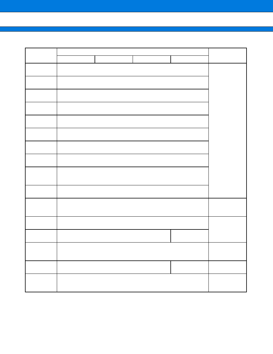
MB91360G Series
53
(Continued)
Address
Register
Block
+
+
+
+
0
+
+
+
+
1
+
+
+
+
2
+
+
+
+
3
000208
H
DMACA1 [R/W]
00000000 0000XXXX XXXXXXXX XXXXXXXX
DMAC
00020C
H
DMACB1 [R/W]
00000000 00000000 XXXXXXXX XXXXXXXX
000210
H
DMACA2 [R/W]
00000000 0000XXXX XXXXXXXX XXXXXXXX
000214
H
DMACB2 [R/W]
00000000 00000000 XXXXXXXX XXXXXXXX
000218
H
DMACA3 [R/W]
00000000 0000XXXX XXXXXXXX XXXXXXXX
00021C
H
DMACB3 [R/W]
00000000 00000000 XXXXXXXX XXXXXXXX
000220
H
DMACA4 [R/W]
00000000 0000XXXX XXXXXXXX XXXXXXXX
000224
H
DMACB4 [R/W]
00000000 00000000 XXXXXXXX XXXXXXXX
000228
H
to
00023C
H
000240
H
DMACR [R/W]
00 - - 0000 - - - - - - - - - - - - - - - - - - - - - - - -
000244
H
to
0002FC
H
Reserved
000300
H
IRBS [R/W, R]
00000000 00000001 00100000 - - - - - - - -
Instruction Cache
000304
H
ISIZE [R/W]
- - - - - -11
000308
H
to
0003E0
H
Reserved
0003E4
H
ICHRC [R/W]
0-000000
Instruction Cache
0003E8
H
to
0003EC
H
Reserved
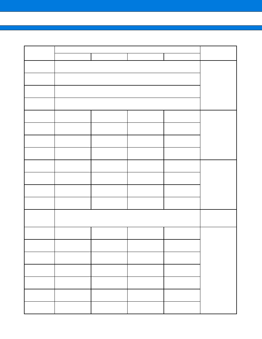
MB91360G Series
54
(Continued)
Address
Register
Block
+
+
+
+
0
+
+
+
+
1
+
+
+
+
2
+
+
+
+
3
0003F0
H
BSD0 [W]
XXXXXXXX XXXXXXXX XXXXXXXX XXXXXXXX
Bit Search
Module
0003F4
H
BSD1 [R/W]
XXXXXXXX XXXXXXXX XXXXXXXX XXXXXXXX
0003F8
H
BSDC [W]
XXXXXXXX XXXXXXXX XXXXXXXX XXXXXXXX
0003FC
H
BSRR [R]
XXXXXXXX XXXXXXXX XXXXXXXX XXXXXXXX
000400
H
DDRG [R/W]
00000000
DDRH [R/W]
00000000
DDRI [R/W]
- - - -0- - -
DDRJ [R/W]
00000000
R-bus
Port Direction
Register
000404
H
DDRK [R/W]
00000000
DDRL [R/W]
00000000
DDRM [R/W]
- - - -0000
DDRN [R/W]
- -000000
000408
H
DDRO [R/W]
00000000
DDRP [R/W]
- - - -0000
DDRQ [R/W]
- -000000
DDRR [R/W]
00000000
00040C
H
DDRS [R/W]
00000000
000410
H
PFRG [R/W]
00000000
PFRH [R/W]
00000000
PFRI [R/W]
- - - -0- - -
PFRJ [R/W]
00000000
R-bus
Port Function
Register
000414
H
PFRK [R/W]
00000000
PFRL [R/W]
00000000
PFRM [R/W]
- - - -0000
PFRN [R/W]
- -000000
000418
H
PFRO [R/W]
00000000
PFRP [R/W]
00000000
PFRQ [R/W]
- -000000
PFRR [R/W]
00000000
00041C
H
PFRS [R/W]
00000000
000420
H
to
00043C
H
Reserved
000440
H
ICR00 [R/W, R]
- - -11111
ICR01 [R/W, R]
- - -11111
ICR02 [R/W, R]
- - -11111
ICR03 [R/W, R]
- - -11111
Interrupt Control
unit
000444
H
ICR04 [R/W, R]
- - -11111
ICR05 [R/W, R]
- - -11111
ICR06 [R/W, R]
- - -11111
ICR07 [R/W, R]
- - -11111
000448
H
ICR08 [R/W, R]
- - -11111
ICR09 [R/W, R]
- - -11111
ICR10 [R/W, R]
- - -11111
ICR11 [R/W, R]
- - -11111
00044C
H
ICR12 [R/W, R]
- - -11111
ICR13 [R/W, R]
- - -11111
ICR14 [R/W, R]
- - -11111
ICR15 [R/W, R]
- - -11111
000450
H
ICR16 [R/W, R]
- - -11111
ICR17 [R/W, R]
- - -11111
ICR18 [R/W, R]
- - -11111
ICR19 [R/W, R]
- - -11111
000454
H
ICR20 [R/W, R]
- - -11111
ICR21 [R/W, R]
- - -11111
ICR22 [R/W, R]
- - -11111
ICR23 [R/W, R]
- - -11111
000458
H
ICR24 [R/W, R]
- - -11111
ICR25 [R/W, R]
- - -11111
ICR26 [R/W, R]
- - -11111
ICR27 [R/W, R]
- - -11111
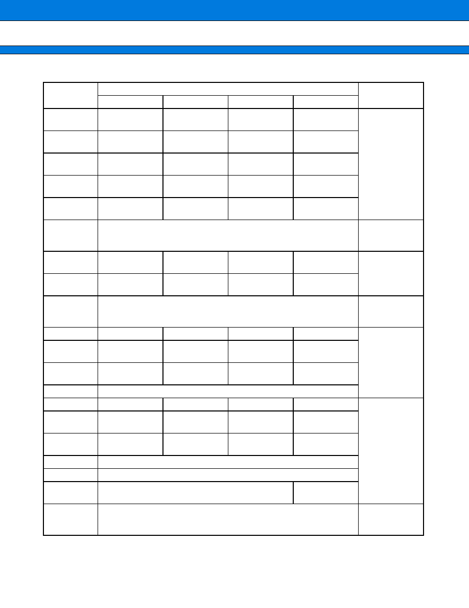
MB91360G Series
55
(Continued)
Address
Register
Block
+
+
+
+
0
+
+
+
+
1
+
+
+
+
2
+
+
+
+
3
00045C
H
ICR28 [R/W, R]
- - -11111
ICR29 [R/W, R]
- - -11111
ICR30 [R/W, R]
- - -11111
ICR31 [R/W, R]
- - -11111
Interrupt Control
unit
000460
H
ICR32 [R/W, R]
- - -11111
ICR33 [R/W, R]
- - -11111
ICR34 [R/W, R]
- - -11111
ICR35 [R/W, R]
- - -11111
000464
H
ICR36 [R/W, R]
- - -11111
ICR37 [R/W, R]
- - -11111
ICR38 [R/W, R]
- - -11111
ICR39 [R/W, R]
- - -11111
000468
H
ICR40 [R/W, R]
- - -11111
ICR41 [R/W, R]
- - -11111
ICR42 [R/W, R]
- - -11111
ICR43 [R/W, R]
- - -11111
00046C
H
ICR44 [R/W, R]
- - -11111
ICR45 [R/W, R]
- - -11111
ICR46 [R/W, R]
- - -11111
ICR47 [R/W, R]
- - -11111
000470
H
to
00047C
H
Reserved
000480
H
RSRR [R/W, R]
10000000
STCR [R/W]
00110011
TBCR [R/W]
X0000X00
CTBR [W]
XXXXXXXX
Clock Control unit
000484
H
CLKR [R/W]
00000000
WPR [W]
XXXXXXXX
DIVR0 [R/W]
00000011
DIVR1 [R/W]
00000000
000488
H
to
0005FC
H
Reserved
000600
H
T-unit
Port Direction
Register
000604
H
DDR7 [R/W]
00000000
000608
H
DDR8 [R/W]
00000000
DDR9 [R/W]
00000000
DDRB [R/W]
00000000
00060C
H
000610
H
T-unit
Port Function
Register
000614
H
PFR7 [R/W]
00001111
000618
H
PFR8 [R/W]
111110-0
PFR9 [R/W]
11110101
PFRB [R/W]
00000000
00061C
H
000620
H
000624
H
PFR27 [R/W]
1111-00-
000628
H
to
00063F
H
Reserved
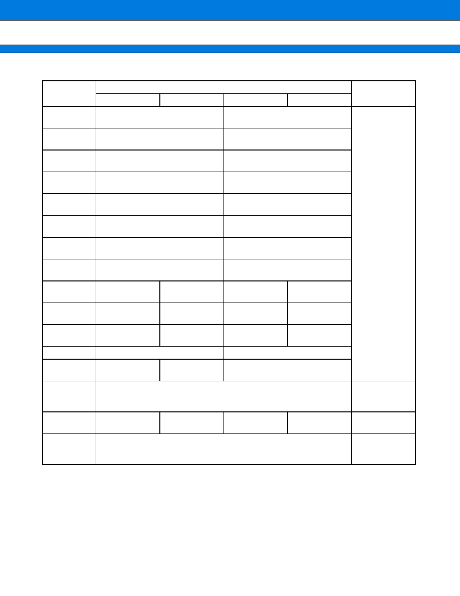
MB91360G Series
56
(Continued)
Address
Register
Block
+
+
+
+
0
+
+
+
+
1
+
+
+
+
2
+
+
+
+
3
000640
H
ASR0 [W]
00000000 00000000
AMR0 [W]
11111000 11111111
T-unit
000644
H
ASR1 [W]
00000000 00000000
AMR1 [W]
00000000 00000000
000648
H
ASR2 [W]
00000000 00000000
AMR2 [W]
00000000 00000000
00064C
H
ASR3 [W]
00000000 00000000
AMR3 [W]
00000000 00000000
000650
H
ASR4 [W]
00000000 00000000
AMR4 [W]
00000000 00000000
000654
H
ASR5 [W]
00000000 00000000
AMR5 [W]
00000000 00000000
000658
H
ASR6 [W]
00000000 00000000
AMR6 [W]
00000000 00000000
00065C
H
ASR7 [W]
00000000 00000000
AMR7 [W]
00000000 00000000
000660
H
AMD0 [R/W]
-00XX111
AMD1 [R/W]
-XXXXXXX
AMD2 [R/W]
-
-XXXXXX
AMD3 [R/W]
-
-XXXXXX
000664
H
AMD4 [R/W]
-
-XXXXXX
AMD5 [R/W]
-
-XXXXXX
AMD6 [R/W]
-XXXXXXX
AMD7 [R/W]
-XXXXXXX
000668
H
CSE
11000011
00066C
H
000670
H
CHE
11111111
000674
H
to
0007F8
H
Reserved
0007FC
H
MODR [W]
XXXXXXXX
Mode Register
000800
H
to
000AFC
H
Reserved

MB91360G Series
57
(Continued)
Address
Register
Block
+
+
+
+
0
+
+
+
+
1
+
+
+
+
2
+
+
+
+
3
000B00
H
ESTS0
X0000000
ESTS1
XXXXXXXX
ESTS2
XXXXXXXX
DSU
000B04
H
ECTL0
0X000000
ECTL1
00000000
ECTL2
000X0000
ECTL3
00000X11
000B08
H
ECNT0
XXXXXXXX
ECNT1
XXXXXXXX
EUSA
XXX0000X
EDTC
0000XXXX
000B0C
H
EWPT
XXXXXXXX XXXXXXXX
000B10
H
EDTR0
XXXXXXXX XXXXXXXX
EDTR1
XXXXXXXX XXXXXXXX
000B14
H
to
000B1C
H
000B20
H
EIA0
XXXXXXXX XXXXXXXX XXXXXXXX XXXXXXXX
000B24
H
EIA1
XXXXXXXX XXXXXXXX XXXXXXXX XXXXXXXX
000B28
H
EIA2
XXXXXXXX XXXXXXXX XXXXXXXX XXXXXXXX
000B2C
H
EIA3
XXXXXXXX XXXXXXXX XXXXXXXX XXXXXXXX
000B30
H
EIA4
XXXXXXXX XXXXXXXX XXXXXXXX XXXXXXXX
000B34
H
EIA5
XXXXXXXX XXXXXXXX XXXXXXXX XXXXXXXX
000B38
H
EIA6
XXXXXXXX XXXXXXXX XXXXXXXX XXXXXXXX
000B3C
H
EIA7
XXXXXXXX XXXXXXXX XXXXXXXX XXXXXXXX
000B40
H
EDTA
XXXXXXXX XXXXXXXX XXXXXXXX XXXXXXXX
000B44
H
EDTM
XXXXXXXX XXXXXXXX XXXXXXXX XXXXXXXX
000B48
H
EOA0
XXXXXXXX XXXXXXXX XXXXXXXX XXXXXXXX
000B4C
H
EOA1
XXXXXXXX XXXXXXXX XXXXXXXX XXXXXXXX
000B50
H
EPCR
XXXXXXXX XXXXXXXX XXXXXXXX XXXXXXXX
000B54
H
EPSR
XXXXXXXX XXXXXXXX XXXXXXXX XXXXXXXX
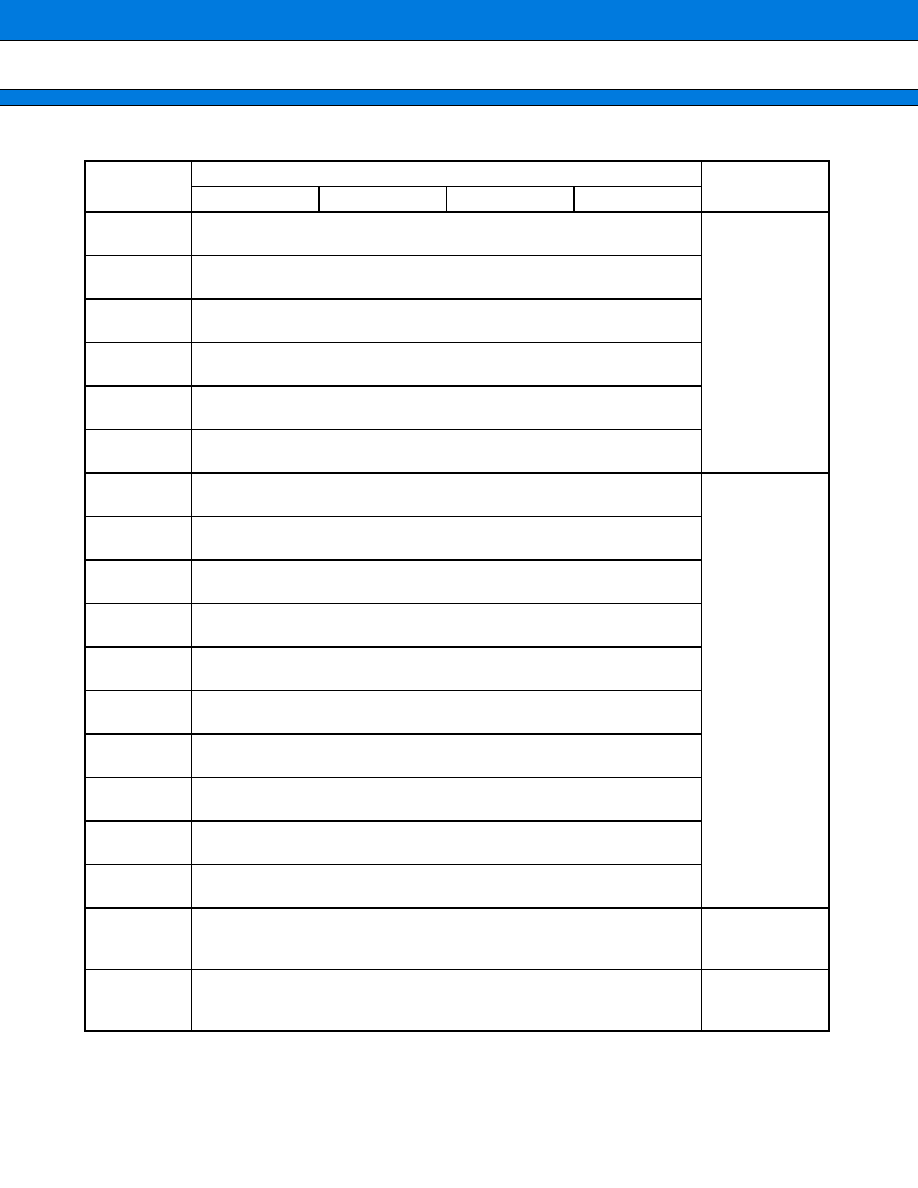
MB91360G Series
58
(Continued)
Address
Register
Block
+
+
+
+
0
+
+
+
+
1
+
+
+
+
2
+
+
+
+
3
000B58
H
EIAM0
XXXXXXXX XXXXXXXX XXXXXXXX XXXXXXXX
DSU
000B5C
H
EIAM1
XXXXXXXX XXXXXXXX XXXXXXXX XXXXXXXX
000B60
H
EOAM0/EODM0
XXXXXXXX XXXXXXXX XXXXXXXX XXXXXXXX
000B64
H
EOAM1/EODM1
XXXXXXXX XXXXXXXX XXXXXXXX XXXXXXXX
000B68
H
EOD0
XXXXXXXX XXXXXXXX XXXXXXXX XXXXXXXX
000B6C
H
EOD1
XXXXXXXX XXXXXXXX XXXXXXXX XXXXXXXX
001000
H
DMASA0 [R/W]
XXXXXXXX XXXXXXXX XXXXXXXX XXXXXXXX
DMAC
001004
H
DMADA0 [R/W]
XXXXXXXX XXXXXXXX XXXXXXXX XXXXXXXX
001008
H
DMASA1 [R/W]
XXXXXXXX XXXXXXXX XXXXXXXX XXXXXXXX
00100C
H
DMADA1 [R/W]
XXXXXXXX XXXXXXXX XXXXXXXX XXXXXXXX
001010
H
DMASA2 [R/W]
XXXXXXXX XXXXXXXX XXXXXXXX XXXXXXXX
001014
H
DMADA2 [R/W]
XXXXXXXX XXXXXXXX XXXXXXXX XXXXXXXX
001018
H
DMASA3 [R/W]
XXXXXXXX XXXXXXXX XXXXXXXX XXXXXXXX
00101C
H
DMADA3 [R/W]
XXXXXXXX XXXXXXXX XXXXXXXX XXXXXXXX
001020
H
DMASA4 [R/W]
XXXXXXXX XXXXXXXX XXXXXXXX XXXXXXXX
001024
H
DMADA4 [R/W]
XXXXXXXX XXXXXXXX XXXXXXXX XXXXXXXX
001028
H
to
003FFC
H
Reserved
004000
H
to
006FFF
H
Reserved
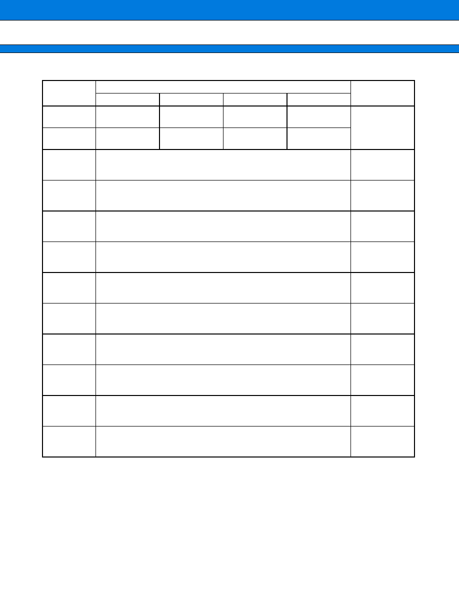
MB91360G Series
59
(Continued)
Address
Register
Block
+
+
+
+
0
+
+
+
+
1
+
+
+
+
2
+
+
+
+
3
007000
H
FMCS [R/W]
1110X000
Flash Memory
Control
Register
007004
H
FMWT [R/W]
- -000011
007008
H
to
00FFFC
H
Reserved
010000
H
to
010FFC
H
(for exact address range see chapter about I-cache)
on F362GA and F369GA no cache, but 4 K I-RAM are available
I-Cache 4 KB
011000
H
to
011FFC
H
Reserved
012000
H
to
01FFFC
H
Reserved
020000
H
to
03BFFC
H
Reserved
03C000
H
to
03FFFC
H
Only first 12 KB are available on F362GA
User RAM
16 KB
(D-Bus)
040000
H
to
043FFC
H
Only first 4 K are available on F362GA
Fast RAM
16 KB
(F-Bus)
044000
H
to
0FEFFC
Reserved
050000
H
to
0507FC
H
Boot ROM
2 KB
(F-Bus)
050800
H
to
07FFF4
H
reserved
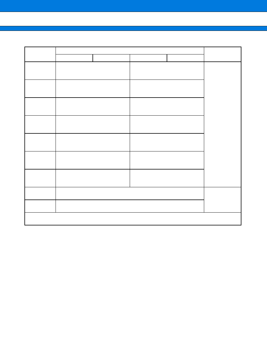
MB91360G Series
60
(Continued)
Address
Register
Block
+
+
+
+
0
+
+
+
+
1
+
+
+
+
2
+
+
+
+
3
080000
H
to
09FFFC
H
Sector 0
64 KB
Sector 7
64 KB
Flash Memory
512 K
on F-Bus
0A0000
H
to
0BFFFC
Sector 1
64 KB
Sector 8
64 KB
0C0000
H
to
0DFFFC
Sector 2
64 KB
Sector 9
64 KB
0E0000
H
to
0EFFFC
Sector 3
32 KB
Sector 10
32 KB
0F0000
H
to
0F3FFC
H
Sector 4
8 KB
Sector 11
8 KB
0F4000
H
to
0F7FFC
H
Sector 5
8 KB
Sector 12
8 KB
0F8000
H
to
0FFFF4
H
Sector 6
16 KB
Sector 13
16 KB
0FFFF8
H
FMV [R]
06 00 00 00
H
Fixed
Reset/Mode
Vector
0FFFFC
H
FRV [R]
00 05 00 00
H
Write operations to address 0FFFF8
H
and 0FFFFC
H
are not possible. When reading these addresses, the values
shown above will be read.
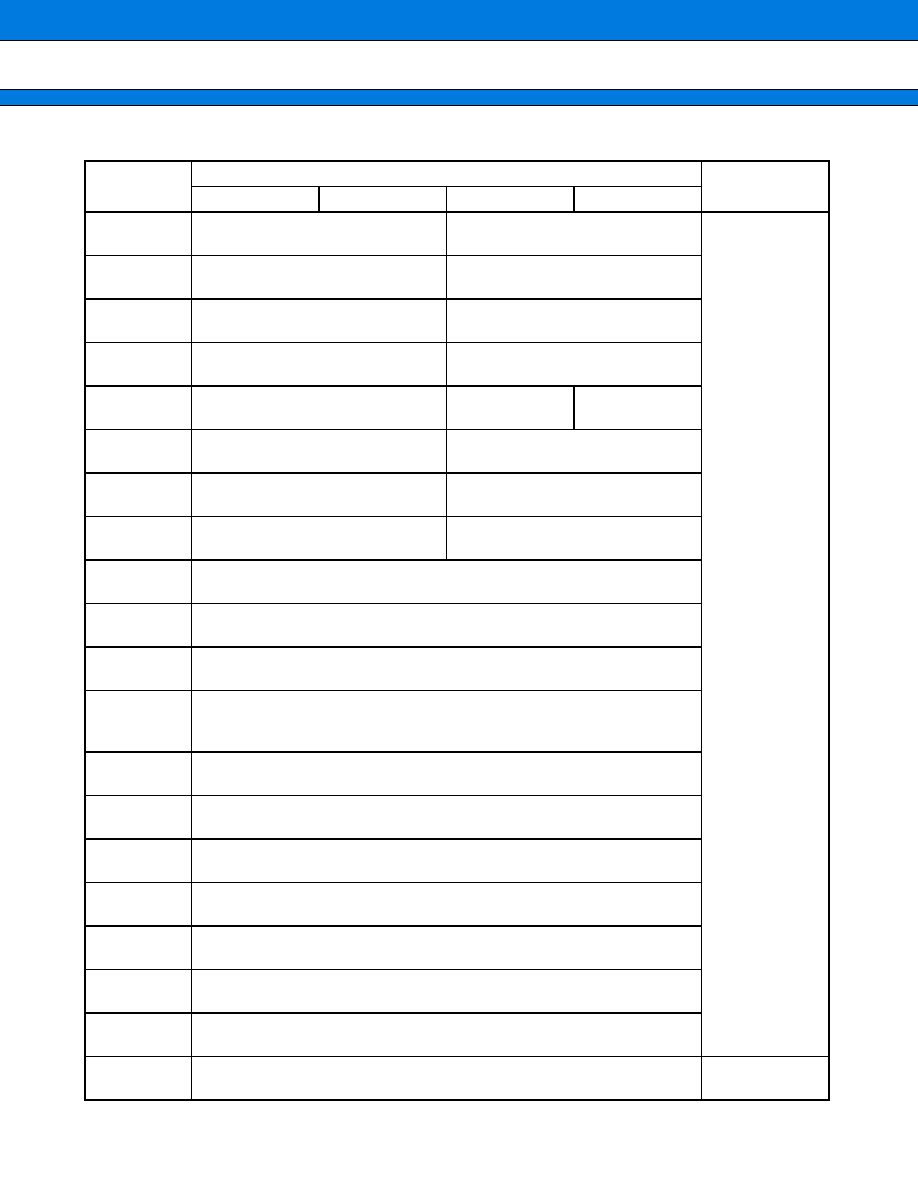
MB91360G Series
61
(Continued)
Address
Register
Block
+
+
+
+
0
+
+
+
+
1
+
+
+
+
2
+
+
+
+
3
100000
H
BVALR0 [R/W]
00000000 00000000
TREQR0 [R/W]
00000000 00000000
CAN 0
Remark :
Address range for
CAN 0 to CAN 3
depends on chip
select range.
Mentioned
addresses are
default values,
determined by
boot ROM
contents.
100004
H
TCANR0 [W]
00000000 00000000
TCR0 [R/W]
00000000 00000000
100008
H
RCR0 [R/W]
00000000 00000000
RRTRR0 [R/W]
00000000 00000000
10000C
H
ROVRR0 [R/W]
00000000 00000000
RIER0 [R/W]
00000000 00000000
100010
H
CSR0 [R/W, R]
00000000 00000001
LEIR0 [R/W]
000-0000
100014
H
RTEC0 [R]
00000000 00000000
BTR0 [R/W]
-1111111 11111111
100018
H
IDER0 [R/W]
XXXXXXXX XXXXXXXX
TRTRR0 [R/W]
00000000 00000000
10001C
H
RFWTR0 [R/W]
XXXXXXXX XXXXXXXX
TIER0 [R/W]
00000000 00000000
100020
H
AMSR0 [R/W]
XXXXXXXX XXXXXXXX XXXXXXXX XXXXXXXX
100024
H
AMR00 [R/W]
XXXXXXXX XXXXXXXX XXXXX
-
-
- XXXXXXXX
100028
H
AMR10 [R/W]
XXXXXXXX XXXXXXXX XXXXX
-
-
- XXXXXXXX
10002C
H
to
100048
H
GENERAL PURPOSE RAM [R/W]
10004C
H
IDR00 [R/W]
XXXXXXXX XXXXXXXX XXXXX
-
-
- XXXXXXXX
100050
H
IDR10 [R/W]
XXXXXXXX XXXXXXXX XXXXX
-
-
- XXXXXXXX
100054
H
IDR20 [R/W]
XXXXXXXX XXXXXXXX XXXXX
-
-
- XXXXXXXX
100058
H
IDR30 [R/W]
XXXXXXXX XXXXXXXX XXXXX
-
-
- XXXXXXXX
10005C
H
IDR40 [R/W]
XXXXXXXX XXXXXXXX XXXXX
-
-
- XXXXXXXX
100060
H
IDR50 [R/W]
XXXXXXXX XXXXXXXX XXXXX
-
-
- XXXXXXXX
100064
H
IDR60 [R/W]
XXXXXXXX XXXXXXXX XXXXX
-
-
- XXXXXXXX
100068
H
IDR70 [R/W]
XXXXXXXX XXXXXXXX XXXXX
-
-
- XXXXXXXX
CAN 0
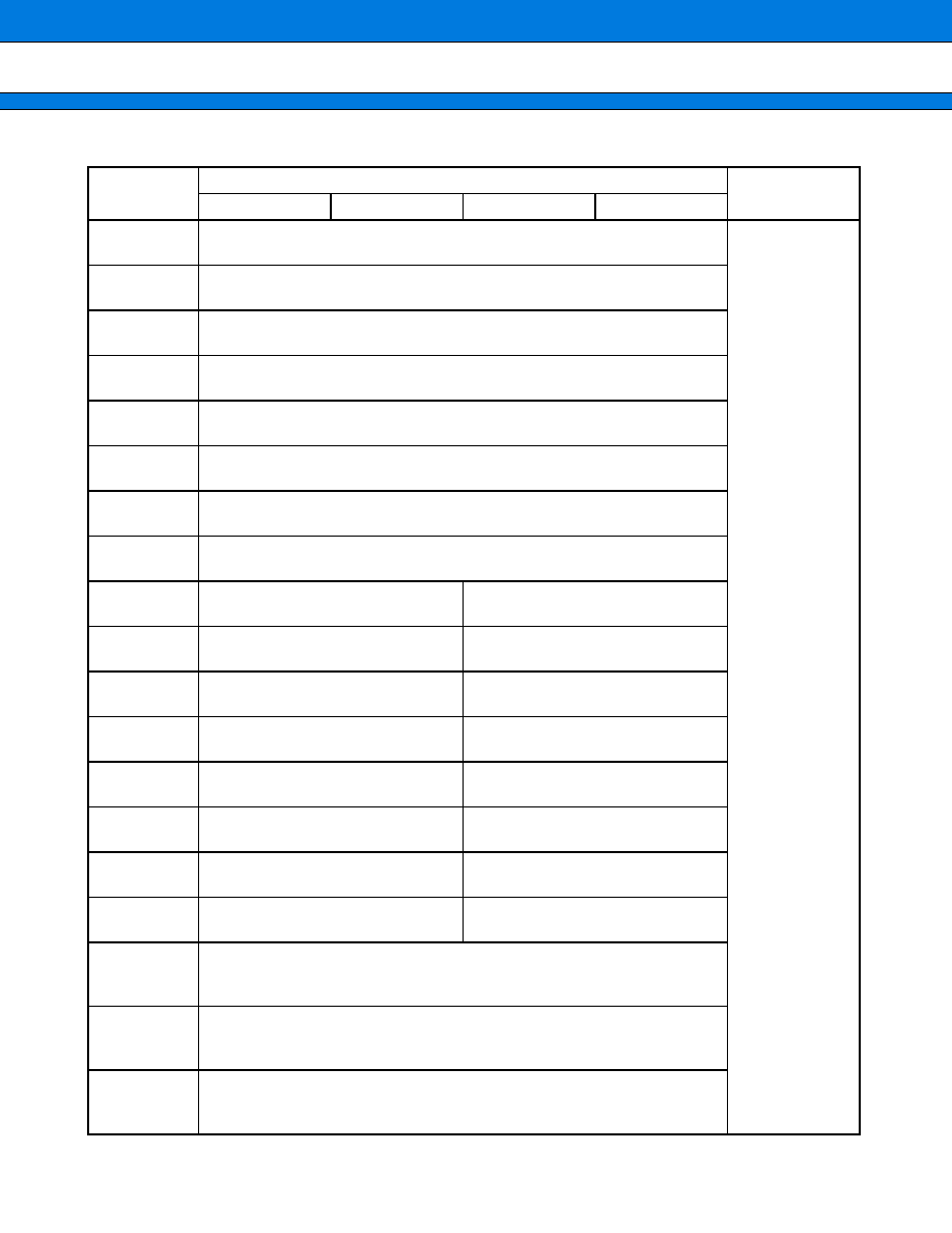
MB91360G Series
62
(Continued)
Address
Register
Block
+
+
+
+
0
+
+
+
+
1
+
+
+
+
2
+
+
+
+
3
10006C
H
IDR80 [R/W]
XXXXXXXX XXXXXXXX XXXXX
-
-
- XXXXXXXX
CAN 0
100070
H
IDR90 [R/W]
XXXXXXXX XXXXXXXX XXXXX
-
-
- XXXXXXXX
100074
H
IDR100 [R/W]
XXXXXXXX XXXXXXXX XXXXX
-
-
- XXXXXXXX
100078
H
IDR110 [R/W]
XXXXXXXX XXXXXXXX XXXXX
-
-
- XXXXXXXX
10007C
H
IDR120 [R/W]
XXXXXXXX XXXXXXXX XXXXX
-
-
- XXXXXXXX
100080
H
IDR130 [R/W]
XXXXXXXX XXXXXXXX XXXXX
-
-
- XXXXXXXX
100084
H
IDR140 [R/W]
XXXXXXXX XXXXXXXX XXXXX
-
-
- XXXXXXXX
100088
H
IDR150 [R/W]
XXXXXXXX XXXXXXXX XXXXX
-
-
- XXXXXXXX
10008C
H
DLCR00 [R/W]
- - - - - - - - -
-
-
-
XXXX
DLCR10 [R/W]
- - - - - - - - -
-
-
-
XXXX
100090
H
DLCR20 [R/W]
- - - - - - - - -
-
-
-
XXXX
DLCR30 [R/W]
- - - - - - - - -
-
-
-
XXXX
100094
H
DLCR40 [R/W]
- - - - - - - - -
-
-
-
XXXX
DLCR50 [R/W]
- - - - - - - - -
-
-
-
XXXX
100098
H
DLCR60 [R/W]
- - - - - - - - -
-
-
-
XXXX
DLCR70 [R/W]
- - - - - - - - -
-
-
-
XXXX
10009C
H
DLCR80 [R/W]
- - - - - - - - -
-
-
-
XXXX
DLCR90 [R/W]
- - - - - - - - -
-
-
-
XXXX
1000A0
H
DLCR100 [R/W]
- - - - - - - - -
-
-
-
XXXX
DLCR110 [R/W]
- - - - - - - - -
-
-
-
XXXX
1000A4
H
DLCR120 [R/W]
- - - - - - - - -
-
-
-
XXXX
DLCR130 [R/W]
- - - - - - - - -
-
-
-
XXXX
1000A8
H
DLCR140 [R/W]
- - - - - - - - -
-
-
-
XXXX
DLCR150 [R/W]
- - - - - - - - -
-
-
-
XXXX
1000AC
H
DTR00 [R/W]
XXXXXXXX XXXXXXXX XXXXXXXX XXXXXXXX
XXXXXXXX XXXXXXXX XXXXXXXX XXXXXXXX
1000B4
H
DTR10 [R/W]
XXXXXXXX XXXXXXXX XXXXXXXX XXXXXXXX
XXXXXXXX XXXXXXXX XXXXXXXX XXXXXXXX
1000BC
H
DTR20 [R/W]
XXXXXXXX XXXXXXXX XXXXXXXX XXXXXXXX
XXXXXXXX XXXXXXXX XXXXXXXX XXXXXXXX
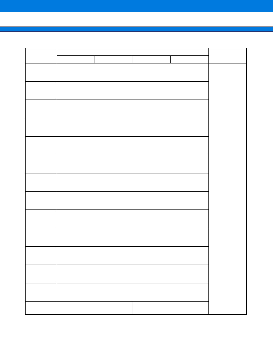
MB91360G Series
63
(Continued)
Address
Register
Block
+
+
+
+
0
+
+
+
+
1
+
+
+
+
2
+
+
+
+
3
1000C4
H
DTR30 [R/W]
XXXXXXXX XXXXXXXX XXXXXXXX XXXXXXXX
XXXXXXXX XXXXXXXX XXXXXXXX XXXXXXXX
CAN 0
1000CC
H
DTR40 [R/W]
XXXXXXXX XXXXXXXX XXXXXXXX XXXXXXXX
XXXXXXXX XXXXXXXX XXXXXXXX XXXXXXXX
1000D4
H
DTR50 [R/W]
XXXXXXXX XXXXXXXX XXXXXXXX XXXXXXXX
XXXXXXXX XXXXXXXX XXXXXXXX XXXXXXXX
1000DC
H
DTR60 [R/W]
XXXXXXXX XXXXXXXX XXXXXXXX XXXXXXXX
XXXXXXXX XXXXXXXX XXXXXXXX XXXXXXXX
1000E4
H
DTR70 [R/W]
XXXXXXXX XXXXXXXX XXXXXXXX XXXXXXXX
XXXXXXXX XXXXXXXX XXXXXXXX XXXXXXXX
1000EC
H
DTR80 [R/W]
XXXXXXXX XXXXXXXX XXXXXXXX XXXXXXXX
XXXXXXXX XXXXXXXX XXXXXXXX XXXXXXXX
1000F4
H
DTR90 [R/W]
XXXXXXXX XXXXXXXX XXXXXXXX XXXXXXXX
XXXXXXXX XXXXXXXX XXXXXXXX XXXXXXXX
1000FC
H
DTR100 [R/W]
XXXXXXXX XXXXXXXX XXXXXXXX XXXXXXXX
XXXXXXXX XXXXXXXX XXXXXXXX XXXXXXXX
100104
H
DTR110 [R/W]
XXXXXXXX XXXXXXXX XXXXXXXX XXXXXXXX
XXXXXXXX XXXXXXXX XXXXXXXX XXXXXXXX
10010C
H
DTR120 [R/W]
XXXXXXXX XXXXXXXX XXXXXXXX XXXXXXXX
XXXXXXXX XXXXXXXX XXXXXXXX XXXXXXXX
100114
H
DTR130 [R/W]
XXXXXXXX XXXXXXXX XXXXXXXX XXXXXXXX
XXXXXXXX XXXXXXXX XXXXXXXX XXXXXXXX
10011C
H
DTR140 [R/W]
XXXXXXXX XXXXXXXX XXXXXXXX XXXXXXXX
XXXXXXXX XXXXXXXX XXXXXXXX XXXXXXXX
100124
H
DTR150 [R/W]
XXXXXXXX XXXXXXXX XXXXXXXX XXXXXXXX
XXXXXXXX XXXXXXXX XXXXXXXX XXXXXXXX
10012C
H
CREG0 [R/W]
00000000 00000110
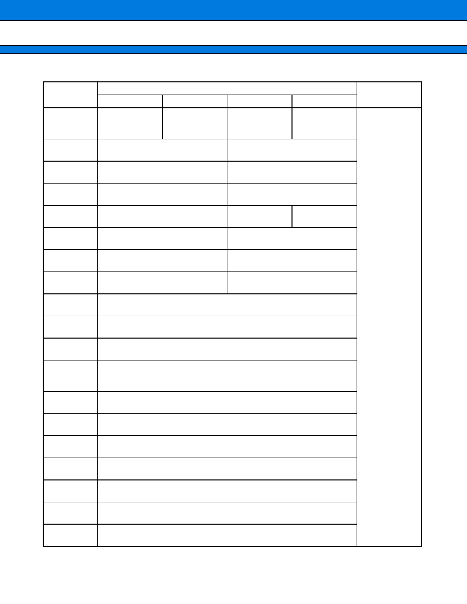
MB91360G Series
64
(Continued)
Address
Register
Block
+
+
+
+
0
+
+
+
+
1
+
+
+
+
2
+
+
+
+
3
100200
H
BVALR1 [R/W]
00000000
00000000
TREQR1 [R/W]
00000000
00000000
CAN 1
Remark :
Address range for
CAN 0 to CAN 3
depends on chip
select range.
Mentioned
addresses are
default values,
determined by
boot ROM
contents.
100204
H
TCANR1 [W]
00000000 00000000
TCR1 [R/W]
00000000 00000000
100208
H
RCR1 [R/W]
00000000 00000000
RRTRR1 [R/W]
00000000 00000000
10020C
H
ROVRR1 [R/W]
00000000 00000000
RIER1 [R/W]
00000000 00000000
100210
H
CSR1 [R/W, R]
00000000 00000001
LEIR1 [R/W]
000-0000
100214
H
RTEC1 [R]
00000000 00000000
BTR1 [R/W]
-1111111 11111111
100218
H
IDER1 [R/W]
XXXXXXXX XXXXXXXX
TRTRR1 [R/W]
00000000 00000000
10021C
H
RFWTR1 [R/W]
XXXXXXXX XXXXXXXX
TIER1 [R/W]
00000000 00000000
100220
H
AMSR1 [R/W]
XXXXXXXX XXXXXXXX XXXXXXXX XXXXXXXX
100224
H
AMR01 [R/W]
XXXXXXXX XXXXXXXX XXXXX
-
-
- XXXXXXXX
100228
H
AMR11 [R/W]
XXXXXXXX XXXXXXXX XXXXX
-
-
- XXXXXXXX
10022C
H
to
100248
H
GENERAL PURPOSE RAM [R/W]
10024C
H
IDR01 [R/W]
XXXXXXXX XXXXXXXX XXXXX
-
-
- XXXXXXXX
100250
H
IDR11 [R/W]
XXXXXXXX XXXXXXXX XXXXX
-
-
- XXXXXXXX
100254
H
IDR21[R/W]
XXXXXXXX XXXXXXXX XXXXX
-
-
- XXXXXXXX
100258
H
IDR31 [R/W]
XXXXXXXX XXXXXXXX XXXXX
-
-
- XXXXXXXX-
10025C
H
IDR41 [R/W]
XXXXXXXX XXXXXXXX XXXXX
-
-
- XXXXXXXX
100260
H
IDR51 [R/W]
XXXXXXXX XXXXXXXX XXXXX
-
-
- XXXXXXXX
100264
H
IDR61 [R/W]
XXXXXXXX XXXXXXXX XXXXX
-
-
- XXXXXXXX
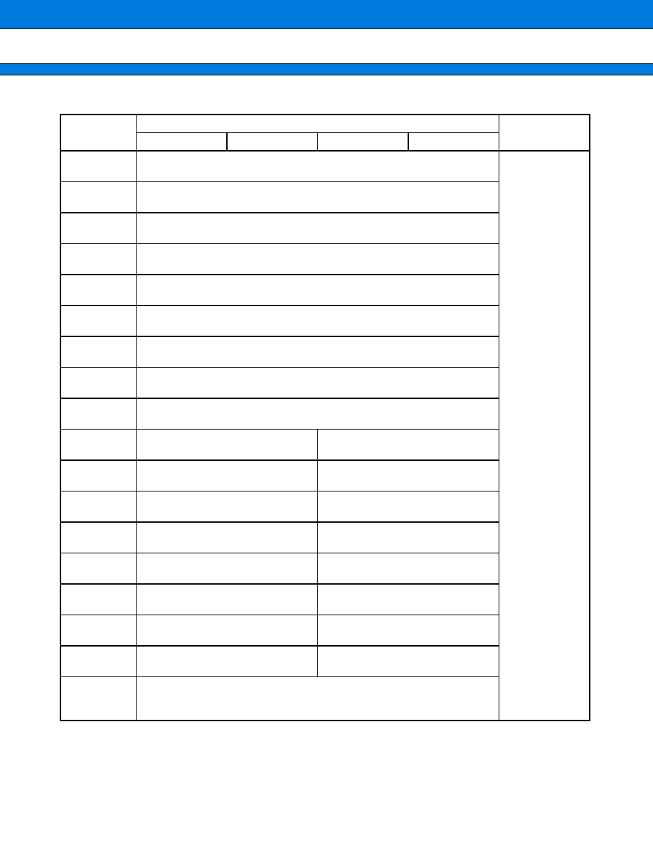
MB91360G Series
65
(Continued)
Address
Register
Block
+
+
+
+
0
+
+
+
+
1
+
+
+
+
2
+
+
+
+
3
100268
H
IDR71 [R/W]
XXXXXXXX XXXXXXXX XXXXX
-
-
- XXXXXXXX
CAN 1
10026C
H
IDR81 [R/W]
XXXXXXXX XXXXXXXX XXXXX
-
-
- XXXXXXXX
100270
H
IDR91 [R/W]
XXXXXXXX XXXXXXXX XXXXX
-
-
- XXXXXXXX
100274
H
IDR101 [R/W]
XXXXXXXX XXXXXXXX XXXXX
-
-
- XXXXXXXX
100278
H
IDR111 [R/W]
XXXXXXXX XXXXXXXX XXXXX
-
-
- XXXXXXXX
10027C
H
IDR121 [R/W]
XXXXXXXX XXXXXXXX XXXXXXXX XXXXX
-
-
-
100280
H
IDR131 [R/W]
XXXXXXXX XXXXXXXX XXXXX
-
-
- XXXXXXXX
100284
H
IDR141 [R/W]
XXXXXXXX XXXXXXXX XXXXX
-
-
- XXXXXXXX
100288
H
IDR151 [R/W]
XXXXXXXX XXXXXXXX XXXXX
-
-
- XXXXXXXX
10028C
H
DLCR01 [R/W]
- - - - - - - - -
-
-
-
XXXX
DLCR11 [R/W]
- - - - - - - - -
-
-
-
XXXX
100290
H
DLCR21 [R/W]
- - - - - - - - -
-
-
-
XXXX
DLCR31 [R/W]
- - - - - - - - -
-
-
-
XXXX
100294
H
DLCR41 [R/W]
- - - - - - - - -
-
-
-
XXXX
DLCR51 [R/W]
- - - - - - - - -
-
-
-
XXXX
100298
H
DLCR61 [R/W]
- - - - - - - - -
-
-
-
XXXX
DLCR71 [R/W]
- - - - - - - - -
-
-
-
XXXX
10029C
H
DLCR81[R/W]
- - - - - - - - -
-
-
-
XXXX
DLCR91 [R/W]
- - - - - - - - -
-
-
-
XXXX
1002A0
H
DLCR101 [R/W]
- - - - - - - - -
-
-
-
XXXX
DLCR111 [R/W]
- - - - - - - - -
-
-
-
XXXX
1002A4
H
DLCR121 [R/W]
- - - - - - - - -
-
-
-
XXXX
DLCR131 [R/W]
- - - - - - - - -
-
-
-
XXXX
1002A8
H
DLCR141 [R/W]
- - - - - - - - -
-
-
-
XXXX
DLCR151 [R/W]
- - - - - - - - -
-
-
-
XXXX
1002AC
H
DTR01 [R/W]
XXXXXXXX XXXXXXXX XXXXXXXX XXXXXXXX
XXXXXXXX XXXXXXXX XXXXXXXX XXXXXXXX
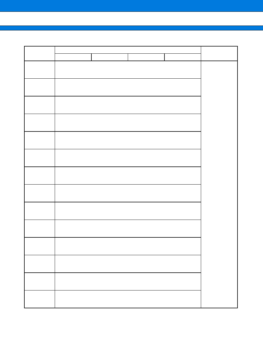
MB91360G Series
66
(Continued)
Address
Register
Block
+
+
+
+
0
+
+
+
+
1
+
+
+
+
2
+
+
+
+
3
1002B4
H
DTR11 [R/W]
XXXXXXXX XXXXXXXX XXXXXXXX XXXXXXXX
XXXXXXXX XXXXXXXX XXXXXXXX XXXXXXXX
CAN 1
1002BC
H
DTR21 [R/W]
XXXXXXXX XXXXXXXX XXXXXXXX XXXXXXXX
XXXXXXXX XXXXXXXX XXXXXXXX XXXXXXXX
1002C4
H
DTR31 [R/W]
XXXXXXXX XXXXXXXX XXXXXXXX XXXXXXXX
XXXXXXXX XXXXXXXX XXXXXXXX XXXXXXXX
1002CC
H
DTR41 [R/W]
XXXXXXXX XXXXXXXX XXXXXXXX XXXXXXXX
XXXXXXXX XXXXXXXX XXXXXXXX XXXXXXXX
1002D4
H
DTR51 [R/W]
XXXXXXXX XXXXXXXX XXXXXXXX XXXXXXXX
XXXXXXXX XXXXXXXX XXXXXXXX XXXXXXXX
1002DC
H
DTR61 [R/W]
XXXXXXXX XXXXXXXX XXXXXXXX XXXXXXXX
XXXXXXXX XXXXXXXX XXXXXXXX XXXXXXXX
1002E4
H
DTR71 [R/W]
XXXXXXXX XXXXXXXX XXXXXXXX XXXXXXXX
XXXXXXXX XXXXXXXX XXXXXXXX XXXXXXXX
1002EC
H
DTR81 [R/W]
XXXXXXXX XXXXXXXX XXXXXXXX XXXXXXXX
XXXXXXXX XXXXXXXX XXXXXXXX XXXXXXXX
1002F4
H
DTR91 [R/W]
XXXXXXXX XXXXXXXX XXXXXXXX XXXXXXXX
XXXXXXXX XXXXXXXX XXXXXXXX XXXXXXXX
1002FC
H
DTR101 [R/W]
XXXXXXXX XXXXXXXX XXXXXXXX XXXXXXXX
XXXXXXXX XXXXXXXX XXXXXXXX XXXXXXXX
100304
H
DTR111 [R/W]
XXXXXXXX XXXXXXXX XXXXXXXX XXXXXXXX
XXXXXXXX XXXXXXXX XXXXXXXX XXXXXXXX
10030C
H
DTR121 [R/W]
XXXXXXXX XXXXXXXX XXXXXXXX XXXXXXXX
XXXXXXXX XXXXXXXX XXXXXXXX XXXXXXXX
100314
H
DTR131 [R/W]
XXXXXXXX XXXXXXXX XXXXXXXX XXXXXXXX
XXXXXXXX XXXXXXXX XXXXXXXX XXXXXXXX
10031C
H
DTR141 [R/W]
XXXXXXXX XXXXXXXX XXXXXXXX XXXXXXXX
XXXXXXXX XXXXXXXX XXXXXXXX XXXXXXXX
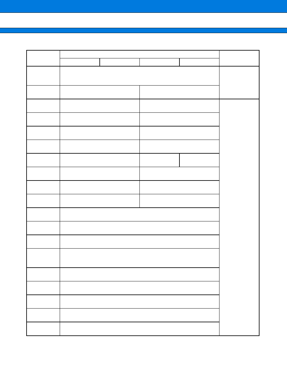
MB91360G Series
67
(Continued)
Address
Register
Block
+
+
+
+
0
+
+
+
+
1
+
+
+
+
2
+
+
+
+
3
100324
H
DTR151 [R/W]
XXXXXXXX XXXXXXXX XXXXXXXX XXXXXXXX
XXXXXXXX XXXXXXXX XXXXXXXX XXXXXXXX
CAN 1
10032C
H
CREG1 [R/W]
00000000 00000110
100400
H
BVALR2 [R/W]
00000000 00000000
TREQR2 [R/W]
00000000 00000000
CAN 2
Remark :
Address range for
CAN 0 to CAN 3
depends on chip
select range.
Mentioned
addresses are
default values,
determined by
boot ROM
contents.
100404
H
TCANR2 [W]
00000000 00000000
TCR2 [R/W]
00000000 00000000
100408
H
RCR2 [R/W]
00000000 00000000
RRTRR1 [R/W]
00000000 00000000
10040C
H
ROVRR2 [R/W]
00000000 00000000
RIER2 [R/W]
00000000 00000000
100410
H
CSR2 [R/W, R]
00000000 00000001
LEIR2 [R/W]
000-0000
100414
H
RTEC2 [R]
00000000 00000000
BTR2 [R/W]
-1111111 11111111
100418
H
IDER2 [R/W]
XXXXXXXX XXXXXXXX
TRTRR2 [R/W]
00000000 00000000
10041C
H
RFWTR2 [R/W]
XXXXXXXX XXXXXXXX
TIER2 [R/W]
00000000 00000000
100420
H
AMSR2 [R/W]
XXXXXXXX XXXXXXXX XXXXXXXX XXXXXXXX
100424
H
AMR02 [R/W]
XXXXXXXX XXXXXXXX XXXXX
-
-
- XXXXXXXX
100428
H
AMR12 [R/W]
XXXXXXXX XXXXXXXX XXXXX
-
-
- XXXXXXXX
10042C
H
to
100448
H
GENERAL PURPOSE RAM [R/W]
10044C
H
IDR02 [R/W]
XXXXXXXX XXXXXXXX XXXXX
-
-
- XXXXXXXX
100450
H
IDR12 [R/W]
XXXXXXXX XXXXXXXX XXXXX
-
-
- XXXXXXXX
100454
H
IDR22[R/W]
XXXXXXXX XXXXXXXX XXXXX
-
-
- XXXXXXXX
100458
H
IDR32 [R/W]
XXXXXXXX XXXXXXXX XXXXX
-
-
- XXXXXXXX-
10045C
H
IDR42 [R/W]
XXXXXXXX XXXXXXXX XXXXX
-
-
- XXXXXXXX

MB91360G Series
68
(Continued)
Address
Register
Block
+
+
+
+
0
+
+
+
+
1
+
+
+
+
2
+
+
+
+
3
100460
H
IDR52 [R/W]
XXXXXXXX XXXXXXXX XXXXX
-
-
- XXXXXXXX
CAN 2
100464
H
IDR62 [R/W]
XXXXXXXX XXXXXXXX XXXXX
-
-
- XXXXXXXX
100468
H
IDR72 [R/W]
XXXXXXXX XXXXXXXX XXXXX
-
-
- XXXXXXXX
10046C
H
IDR82 [R/W]
XXXXXXXX XXXXXXXX XXXXX
-
-
- XXXXXXXX
100470
H
IDR92 [R/W]
XXXXXXXX XXXXXXXX XXXXX
-
-
- XXXXXXXX
100474
H
IDR102 [R/W]
XXXXXXXX XXXXXXXX XXXXX
-
-
- XXXXXXXX
100478
H
IDR112 [R/W]
XXXXXXXX XXXXXXXX XXXXX
-
-
- XXXXXXXX
10047C
H
IDR122 [R/W]
XXXXXXXX XXXXXXXX XXXXXXXX XXXXX
-
-
-
100480
H
IDR132 [R/W]
XXXXXXXX XXXXXXXX XXXXX
-
-
- XXXXXXXX
100484
H
IDR142 [R/W]
XXXXXXXX XXXXXXXX XXXXX
-
-
- XXXXXXXX
100488
H
IDR152 [R/W]
XXXXXXXX XXXXXXXX XXXXX
-
-
- XXXXXXXX
10048C
H
DLCR02 [R/W]
- - - - - - - - -
-
-
-
XXXX
DLCR12 [R/W]
- - - - - - - - -
-
-
-
XXXX
100490
H
DLCR22 [R/W]
- - - - - - - - -
-
-
-
XXXX
DLCR32 [R/W]
- - - - - - - - -
-
-
-
XXXX
100494
H
DLCR42 [R/W]
- - - - - - - - -
-
-
-
XXXX
DLCR52 [R/W]
- - - - - - - - -
-
-
-
XXXX
100498
H
DLCR62 [R/W]
- - - - - - - - -
-
-
-
XXXX
DLCR72 [R/W]
- - - - - - - - -
-
-
-
XXXX
10049C
H
DLCR82[R/W]
- - - - - - - - -
-
-
-
XXXX
DLCR92 [R/W]
- - - - - - - - -
-
-
-
XXXX
1004A0
H
DLCR102 [R/W]
- - - - - - - - -
-
-
-
XXXX
DLCR112 [R/W]
- - - - - - - - -
-
-
-
XXXX
1004A4
H
DLCR122 [R/W]
- - - - - - - - -
-
-
-
XXXX
DLCR132 [R/W]
- - - - - - - - -
-
-
-
XXXX
1004A8
H
DLCR142 [R/W]
- - - - - - - - -
-
-
-
XXXX
DLCR152 [R/W]
- - - - - - - - -
-
-
-
XXXX

MB91360G Series
69
(Continued)
Address
Register
Block
+
+
+
+
0
+
+
+
+
1
+
+
+
+
2
+
+
+
+
3
1004AC
H
DTR02 [R/W]
XXXXXXXX XXXXXXXX XXXXXXXX XXXXXXXX
XXXXXXXX XXXXXXXX XXXXXXXX XXXXXXXX
CAN 2
1004B4
H
DTR12 [R/W]
XXXXXXXX XXXXXXXX XXXXXXXX XXXXXXXX
XXXXXXXX XXXXXXXX XXXXXXXX XXXXXXXX
1004BC
H
DTR22 [R/W]
XXXXXXXX XXXXXXXX XXXXXXXX XXXXXXXX
XXXXXXXX XXXXXXXX XXXXXXXX XXXXXXXX
1004C4
H
DTR32 [R/W]
XXXXXXXX XXXXXXXX XXXXXXXX XXXXXXXX
XXXXXXXX XXXXXXXX XXXXXXXX XXXXXXXX
1004CC
H
DTR42 [R/W]
XXXXXXXX XXXXXXXX XXXXXXXX XXXXXXXX
XXXXXXXX XXXXXXXX XXXXXXXX XXXXXXXX
1004D4
H
DTR52 [R/W]
XXXXXXXX XXXXXXXX XXXXXXXX XXXXXXXX
XXXXXXXX XXXXXXXX XXXXXXXX XXXXXXXX
1004DC
H
DTR62 [R/W]
XXXXXXXX XXXXXXXX XXXXXXXX XXXXXXXX
XXXXXXXX XXXXXXXX XXXXXXXX XXXXXXXX
1004E4
H
DTR72 [R/W]
XXXXXXXX XXXXXXXX XXXXXXXX XXXXXXXX
XXXXXXXX XXXXXXXX XXXXXXXX XXXXXXXX
1004EC
H
DTR82 [R/W]
XXXXXXXX XXXXXXXX XXXXXXXX XXXXXXXX
XXXXXXXX XXXXXXXX XXXXXXXX XXXXXXXX
1004F4
H
DTR92 [R/W]
XXXXXXXX XXXXXXXX XXXXXXXX XXXXXXXX
XXXXXXXX XXXXXXXX XXXXXXXX XXXXXXXX
1004FC
H
DTR102 [R/W]
XXXXXXXX XXXXXXXX XXXXXXXX XXXXXXXX
XXXXXXXX XXXXXXXX XXXXXXXX XXXXXXXX
100504
H
DTR112 [R/W]
XXXXXXXX XXXXXXXX XXXXXXXX XXXXXXXX
XXXXXXXX XXXXXXXX XXXXXXXX XXXXXXXX
10050C
H
DTR122 [R/W]
XXXXXXXX XXXXXXXX XXXXXXXX XXXXXXXX
XXXXXXXX XXXXXXXX XXXXXXXX XXXXXXXX
100514
H
DTR132 [R/W]
XXXXXXXX XXXXXXXX XXXXXXXX XXXXXXXX
XXXXXXXX XXXXXXXX XXXXXXXX XXXXXXXX
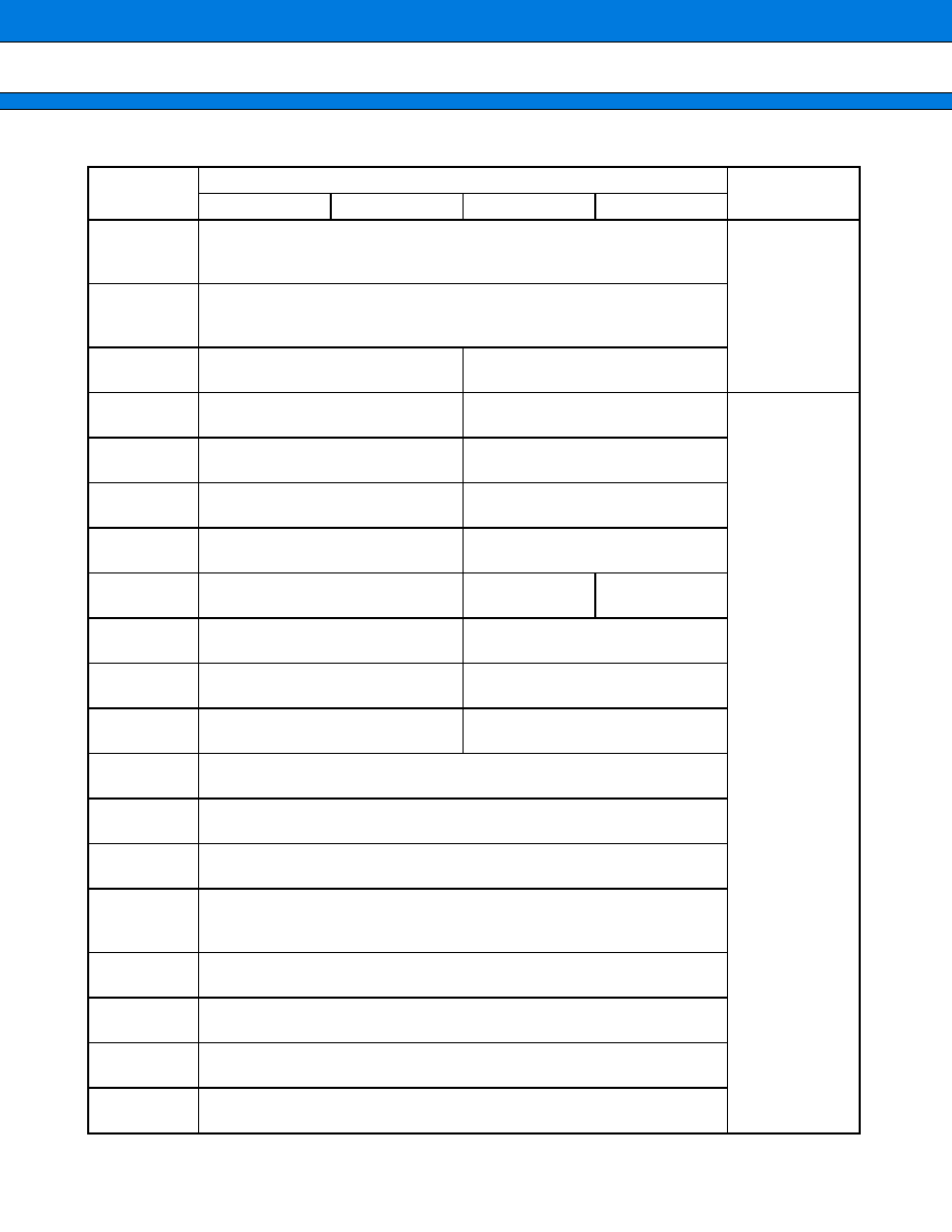
MB91360G Series
70
(Continued)
Address
Register
Block
+
+
+
+
0
+
+
+
+
1
+
+
+
+
2
+
+
+
+
3
10051C
H
DTR142 [R/W]
XXXXXXXX XXXXXXXX XXXXXXXX XXXXXXXX
XXXXXXXX XXXXXXXX XXXXXXXX XXXXXXXX
CAN 2
100524
H
DTR152 [R/W]
XXXXXXXX XXXXXXXX XXXXXXXX XXXXXXXX
XXXXXXXX XXXXXXXX XXXXXXXX XXXXXXXX
10052C
H
CREG2 [R/W]
00000000 00000110
100600
H
BVALR3 [R/W]
00000000 00000000
TREQR3 [R/W]
00000000 00000000
CAN 3
Remark :
Address range for
CAN 0 to CAN 3
depends on chip
select range.
Mentioned
addresses are
default values,
determined by
boot ROM
contents.
100604
H
TCANR3 [W]
00000000 00000000
TCR3 [R/W]
00000000 00000000
100608
H
RCR3 [R/W]
00000000 00000000
RRTRR31 [R/W]
00000000 00000000
10060C
H
ROVRR3 [R/W]
00000000 00000000
RIER3 [R/W]
00000000 00000000
100610
H
CSR3 [R/W, R]
00000000 00000001
LEIR3 [R/W]
000-0000
100614
H
RTEC3 [R]
00000000 00000000
BTR3 [R/W]
-1111111 11111111
100618
H
IDER3 [R/W]
XXXXXXXX XXXXXXXX
TRTRR3 [R/W]
00000000 00000000
10061C
H
RFWTR3 [R/W]
XXXXXXXX XXXXXXXX
TIER3 [R/W]
00000000 00000000
100620
H
AMSR3 [R/W]
XXXXXXXX XXXXXXXX XXXXXXXX XXXXXXXX
100624
H
AMR03 [R/W]
XXXXXXXX XXXXXXXX XXXXX
-
-
- XXXXXXXX
100628
H
AMR13 [R/W]
XXXXXXXX XXXXXXXX XXXXX
-
-
- XXXXXXXX
10062C
H
to
100648
H
GENERAL PURPOSE RAM [R/W]
10064C
H
IDR03 [R/W]
XXXXXXXX XXXXXXXX XXXXX
-
-
- XXXXXXXX
100650
H
IDR13 [R/W]
XXXXXXXX XXXXXXXX XXXXX
-
-
- XXXXXXXX
100654
H
IDR23[R/W]
XXXXXXXX XXXXXXXX XXXXX
-
-
- XXXXXXXX
100658
H
IDR33 [R/W]
XXXXXXXX XXXXXXXX XXXXX
-
-
- XXXXXXXX-
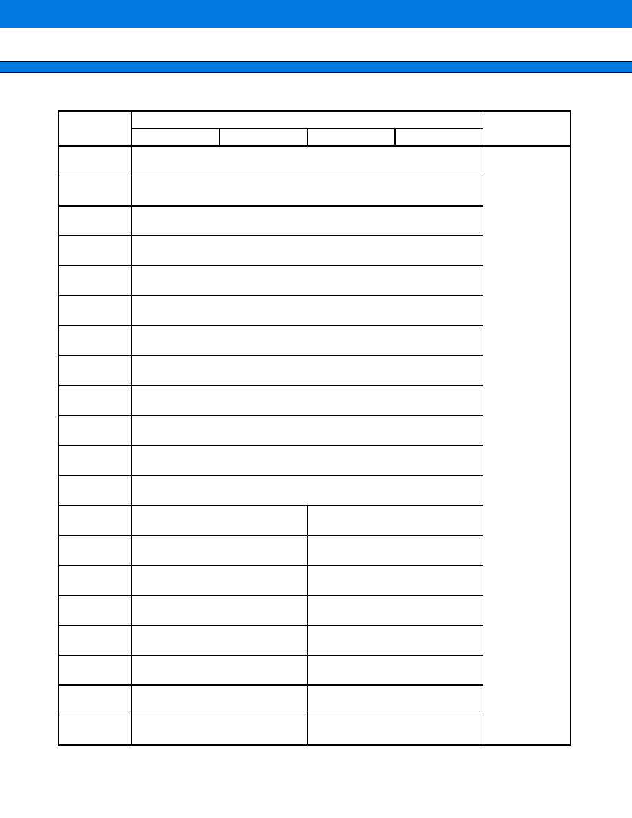
MB91360G Series
71
(Continued)
Address
Register
Block
+
+
+
+
0
+
+
+
+
1
+
+
+
+
2
+
+
+
+
3
10065C
H
IDR43 [R/W]
XXXXXXXX XXXXXXXX XXXXX
-
-
- XXXXXXXX
CAN 3
100660
H
IDR53 [R/W]
XXXXXXXX XXXXXXXX XXXXX
-
-
- XXXXXXXX
100664
H
IDR63 [R/W]
XXXXXXXX XXXXXXXX XXXXX
-
-
- XXXXXXXX
100668
H
IDR73 [R/W]
XXXXXXXX XXXXXXXX XXXXX
-
-
- XXXXXXXX
10066C
H
IDR83 [R/W]
XXXXXXXX XXXXXXXX XXXXX
-
-
- XXXXXXXX
100670
H
IDR93 [R/W]
XXXXXXXX XXXXXXXX XXXXX
-
-
- XXXXXXXX
100674
H
IDR103 [R/W]
XXXXXXXX XXXXXXXX XXXXX
-
-
- XXXXXXXX
100678
H
IDR113 [R/W]
XXXXXXXX XXXXXXXX XXXXX
-
-
- XXXXXXXX
10067C
H
IDR123 [R/W]
XXXXXXXX XXXXXXXX XXXXXXXX XXXXX
-
-
-
100680
H
IDR133 [R/W]
XXXXXXXX XXXXXXXX XXXXX
-
-
- XXXXXXXX
100684
H
IDR143 [R/W]
XXXXXXXX XXXXXXXX XXXXX
-
-
- XXXXXXXX
100688
H
IDR153 [R/W]
XXXXXXXX XXXXXXXX XXXXX
-
-
- XXXXXXXX
10068C
H
DLCR032 [R/W]
- - - - - - - - -
-
-
-
XXXX
DLCR13 [R/W]
- - - - - - - - -
-
-
-
XXXX
100690
H
DLCR232 [R/W]
- - - - - - - - -
-
-
-
XXXX
DLCR33 [R/W]
- - - - - - - - -
-
-
-
XXXX
100694
H
DLCR43 [R/W]
- - - - - - - - -
-
-
-
XXXX
DLCR53 [R/W]
- - - - - - - - -
-
-
-
XXXX
100698
H
DLCR63 [R/W]
- - - - - - - - -
-
-
-
XXXX
DLCR733 [R/W]
- - - - - - - - -
-
-
-
XXXX
10069C
H
DLCR83[R/W]
- - - - - - - - -
-
-
-
XXXX
DLCR93 [R/W]
- - - - - - - - -
-
-
-
XXXX
1006A0
H
DLCR103 [R/W]
- - - - - - - - -
-
-
-
XXXX
DLCR113 [R/W]
- - - - - - - - -
-
-
-
XXXX
1006A4
H
DLCR123 [R/W]
- - - - - - - - -
-
-
-
XXXX
DLCR133 [R/W]
- - - - - - - - -
-
-
-
XXXX
1006A8
H
DLCR143 [R/W]
- - - - - - - - -
-
-
-
XXXX
DLCR153 [R/W]
- - - - - - - - -
-
-
-
XXXX

MB91360G Series
72
(Continued)
Address
Register
Block
+
+
+
+
0
+
+
+
+
1
+
+
+
+
2
+
+
+
+
3
1006AC
H
DTR03 [R/W]
XXXXXXXX XXXXXXXX XXXXXXXX XXXXXXXX
XXXXXXXX XXXXXXXX XXXXXXXX XXXXXXXX
CAN 3
1006B4
H
DTR13 [R/W]
XXXXXXXX XXXXXXXX XXXXXXXX XXXXXXXX
XXXXXXXX XXXXXXXX XXXXXXXX XXXXXXXX
1006BC
H
DTR23 [R/W]
XXXXXXXX XXXXXXXX XXXXXXXX XXXXXXXX
XXXXXXXX XXXXXXXX XXXXXXXX XXXXXXXX
1006C4
H
DTR33 [R/W]
XXXXXXXX XXXXXXXX XXXXXXXX XXXXXXXX
XXXXXXXX XXXXXXXX XXXXXXXX XXXXXXXX
1006CC
H
DTR43 [R/W]
XXXXXXXX XXXXXXXX XXXXXXXX XXXXXXXX
XXXXXXXX XXXXXXXX XXXXXXXX XXXXXXXX
1006D4
H
DTR53 [R/W]
XXXXXXXX XXXXXXXX XXXXXXXX XXXXXXXX
XXXXXXXX XXXXXXXX XXXXXXXX XXXXXXXX
1006DC
H
DTR63 [R/W]
XXXXXXXX XXXXXXXX XXXXXXXX XXXXXXXX
XXXXXXXX XXXXXXXX XXXXXXXX XXXXXXXX
1006E4
H
DTR73 [R/W]
XXXXXXXX XXXXXXXX XXXXXXXX XXXXXXXX
XXXXXXXX XXXXXXXX XXXXXXXX XXXXXXXX
1006EC
H
DTR83 [R/W]
XXXXXXXX XXXXXXXX XXXXXXXX XXXXXXXX
XXXXXXXX XXXXXXXX XXXXXXXX XXXXXXXX
1006F4
H
DTR93 [R/W]
XXXXXXXX XXXXXXXX XXXXXXXX XXXXXXXX
XXXXXXXX XXXXXXXX XXXXXXXX XXXXXXXX
1006FC
H
DTR103 [R/W]
XXXXXXXX XXXXXXXX XXXXXXXX XXXXXXXX
XXXXXXXX XXXXXXXX XXXXXXXX XXXXXXXX
100704
H
DTR113 [R/W]
XXXXXXXX XXXXXXXX XXXXXXXX XXXXXXXX
XXXXXXXX XXXXXXXX XXXXXXXX XXXXXXXX
10070C
H
DTR123 [R/W]
XXXXXXXX XXXXXXXX XXXXXXXX XXXXXXXX
XXXXXXXX XXXXXXXX XXXXXXXX XXXXXXXX
100714
H
DTR133 [R/W]
XXXXXXXX XXXXXXXX XXXXXXXX XXXXXXXX
XXXXXXXX XXXXXXXX XXXXXXXX XXXXXXXX
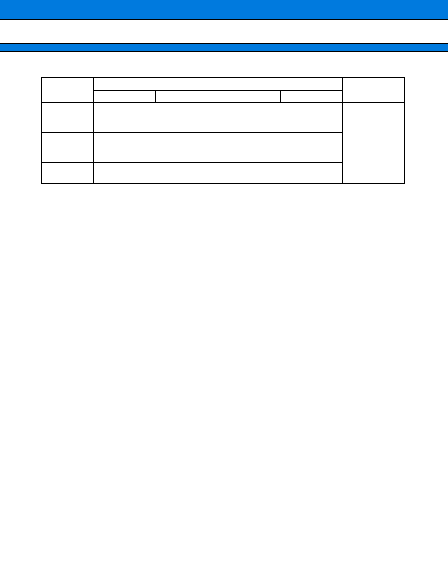
MB91360G Series
73
(Continued)
Address
Register
Block
+
+
+
+
0
+
+
+
+
1
+
+
+
+
2
+
+
+
+
3
10071C
H
DTR143 [R/W]
XXXXXXXX XXXXXXXX XXXXXXXX XXXXXXXX
XXXXXXXX XXXXXXXX XXXXXXXX XXXXXXXX
CAN 3
100724
H
DTR153 [R/W]
XXXXXXXX XXXXXXXX XXXXXXXX XXXXXXXX
XXXXXXXX XXXXXXXX XXXXXXXX XXXXXXXX
10072C
H
CREG3 [R/W]
00000000 00000110
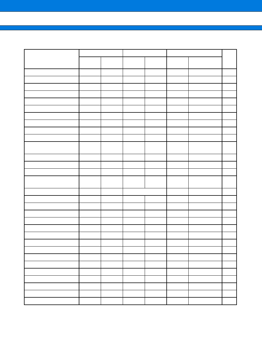
MB91360G Series
74
s
INTERRUPT CAUSES, INTERRUPT VECTORS, AND INTERRUPT CONTROL REGISTER
(Continued)
Interrupt
Interrupt number
Interrupt level
*1
Interrupt vector
*2
RN
Decimal
Hexa-
decimal
Setting
Register
Register
address
Offset
Default Vector
address
Reset
0
00
0x3FC
0x000FFFFC
Mode vector
1
01
0x3F8
0x000FFFF8
System reserved
2
02
0x3F4
0x000FFFF4
System reserved
3
03
0x3F0
0x000FFFF0
System reserved
4
04
0x3EC
0x000FFFEC
System reserved
5
05
0x3E8
0x000FFFE8
System reserved
6
06
0x3E4
0x000FFFE4
Co-processor fault trap
*4
7
07
0x3E0
0x000FFFE0
Co-processor error trap
*4
8
08
0x3DC
0x000FFFDC
INTE instruction
*4
9
09
0x3D8
0x000FFFD8
Instruction break
exception
*4
10
0A
0x3D4
0x000FFFD4
Operand break trap
*4
11
0B
0x3D0
0x000FFFD0
Step trace trap
*4
12
0C
0x3CC
0x000FFFCC
NMI interrupt (tool)
*4
13
0D
0x3C8
0x000FFFC8
Undefined instruction
exception
14
0E
0x3C4
0x000FFFC4
NMI request
15
0F
F
H
fixed
0x3C0
0x000FFFC0
External Interrupt 0
16
10
ICR00
0x440
0x3BC
0x000FFFBC
4
External Interrupt 1
17
11
ICR01
0x441
0x3B8
0x000FFFB8
5
External Interrupt 2
18
12
ICR02
0x442
0x3B4
0x000FFFB4
8
External Interrupt 3
19
13
ICR03
0x443
0x3B0
0x000FFFB0
9
External Interrupt 4
20
14
ICR04
0x444
0x3AC
0x000FFFAC
External Interrupt 5
21
15
ICR05
0x445
0x3A8
0x000FFFA8
External Interrupt 6
22
16
ICR06
0x446
0x3A4
0x000FFFA4
External Interrupt 7
23
17
ICR07
0x447
0x3A0
0x000FFFA0
Reload Timer 0
24
18
ICR08
0x448
0x39C
0x000FFF9C
6
Reload Timer 1
25
19
ICR09
0x449
0x398
0x000FFF98
7
Reload Timer 2
26
1A
ICR10
0x44A
0x394
0x000FFF94
CAN 0 RX
27
1B
ICR11
0x44B
0x390
0x000FFF90
CAN 0 TX/NS
28
1C
ICR12
0x44C
0x38C
0x000FFF8C
CAN 1 RX
29
1D
ICR13
0x44D
0x388
0x000FFF88
CAN 1 TX/NS
30
1E
ICR14
0x44E
0x384
0x000FFF84

MB91360G Series
75
(Continued)
Interrupt
Interrupt number
Interrupt level
*1
Interrupt vector
*2
RN
Decimal
Hexa-
decimal
Setting
Register
Register
address
Offset
Default Vector
address
CAN 2 RX
31
1F
ICR15
0x44F
0x380
0x000FFF80
CAN 2 TX/NS
32
20
ICR16
0x450
0x37C
0x000FFF7C
CAN 3 RX
*5
33
21
ICR17
0x451
0x378
0x000FFF78
CAN 3 TX/NS
*5
34
22
ICR18
0x452
0x374
0x000FFF74
PPG 0/1
35
23
ICR19
0x453
0x370
0x000FFF70
PPG 2/3
36
24
ICR20
0x454
0x36C
0x000FFF6C
PPG 4/5
37
25
ICR21
0x455
0x368
0x000FFF68
PPG 6/7
38
26
ICR22
0x456
0x364
0x000FFF64
Reload Timer 3
39
27
ICR23
0x457
0x360
0x000FFF60
Reload Timer 4
40
28
ICR24
0x458
0x35C
0x000FFF5C
Reload Timer 5
41
29
ICR25
0x459
0x358
0x000FFF58
ICU 0/1
42
2A
ICR26
0x45A
0x354
0x000FFF54
OCU 0/1
43
2B
ICR27
0x45B
0x350
0x000FFF50
ICU 2/3
44
2C
ICR28
0x45C
0x34C
0x000FFF4C
OCU 2/3
45
2D
ICR29
0x45D
0x348
0x000FFF48
ADC
46
2E
ICR30
0x45E
0x344
0x000FFF44
14
Timebase Overflow
47
2F
ICR31
0x45F
0x340
0x000FFF40
Free Running Counter 0
48
30
ICR32
0x460
0x33C
0x000FFF3C
Free Running Counter 1
49
31
ICR33
0x461
0x338
0x000FFF38
SIO 0
*6
50
32
ICR34
0x462
0x334
0x000FFF34
12
SIO 1
*6
51
33
ICR35
0x463
0x330
0x000FFF30
15
Sound Generator
52
34
ICR36
0x464
0x32C
0x000FFF2C
UART 0 RX
53
35
ICR37
0x465
0x328
0x000FFF28
0
UART 0 TX
54
36
ICR38
0x466
0x324
0x000FFF24
1
UART 1 RX
55
37
ICR39
0x467
0x320
0x000FFF20
2
UART 1 TX
56
38
ICR40
0x468
0x31C
0x000FFF1C
3
UART 2 RX
57
39
ICR41
0x469
0x318
0x000FFF18
10
UART 2 TX
58
3A
ICR42
0x46A
0x314
0x000FFF14
11
I
2
C
*7
59
3B
ICR43
0x46B
0x310
0x000FFF10
13
Alarm Comparator
60
3C
ICR44
0x46C
0x30C
0x000FFF0C
RTC (Watchtimer) /
Calibration Unit
61
3D
ICR45
0x46D
0x308
0x000FFF08
DMA
62
3E
ICR46
0x46E
0x304
0x000FFF04
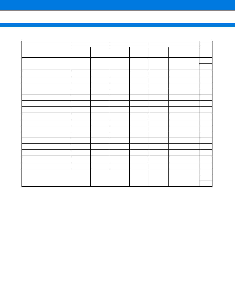
MB91360G Series
76
(Continued)
*1 : The ICRs are located in the interrupt controller and set the interrupt level for each interrupt request. An ICR is
provided for each interrupt request.
*2 : The vector address for each EIT (exception, interrupt or trap) is calculated by adding the listed offset to the table
base register value (TBR) . The TBR specifies the top of the EIT vector table. The addresses listed in the table
are for the default TBR value (0x000FFC00) . The TBR is initialized to this value by a reset.After execution of
the internal boot ROM TBR is set to 0x00FFC00.
*3 : Used by REALOS
*4 : System reserved
*5 : Only available on MB91FV360GA
*6 : DMA to/from SIO only implemented on F369GA.
*7 : DMA to/from I
2
C is not implemented on MB91F362GA.
Remarks :
The 1-Kbyte area from the address specified in TRB is the EIT vector area.
Each vector consists of four bytes. The following formula shows the relationship between the vector number
and vector address.
vector
=
TBR
+
vctofs
=
TBR
+
(3FC
H
-
4
◊
vct)
vctadr : Vector address
vctofs : Vector offset
vct
: Vector number
Interrupt
Interrupt number
Interrupt level
*1
Interrupt vector
*2
RN
Decimal
Hexa-
decimal
Setting
Register
Register
address
Offset
Default Vector
address
Delayed interrupt
activation bit
63
3F
ICR47
0x46F
0x300
0x000FFF00
System reserved
*3
64
40
0x2FC
0x000FFEFC
System reserved
*3
65
41
0x2F8
0x000FFEF8
Security vector
66
42
0x2F4
0x000FFEF4
System reserved
67
43
(ICR51)
0x473
0x2F0
0x000FFEF0
System reserved
68
44
(ICR52)
0x474
0x2EC
0x000FFEEC
System reserved
69
45
(ICR53)
0x475
0x2E8
0x000FFEE8
System reserved
70
46
(ICR54)
0x476
0x2E4
0x000FFEE4
System reserved
71
47
(ICR55)
0x477
0x2E0
0x000FFEE0
System reserved
72
48
(ICR56)
0x478
0x2DC
0x000FFEDC
System reserved
73
49
(ICR57)
0x479
0x2D8
0x000FFED8
System reserved
74
4A
(ICR58)
0x47A
0x2D4
0x000FFED4
System reserved
75
4B
(ICR59)
0x47B
0x2D0
0x000FFED0
System reserved
76
4C
(ICR60)
0x47C
0x2CC
0x000FFECC
System reserved
77
4D
(ICR61)
0x47D
0x2C8
0x000FFEC8
System reserved
78
4E
(ICR62)
0x47E
0x2C4
0x000FFEC4
System reserved
79
4F
(ICR63)
0x47F
0x2C0
0x000FFEC0
Used by the INT
instruction.
80
to
255
50
to
FF
0x2BC
to
0x000
0x000FFEBC
to
0x000FFC00
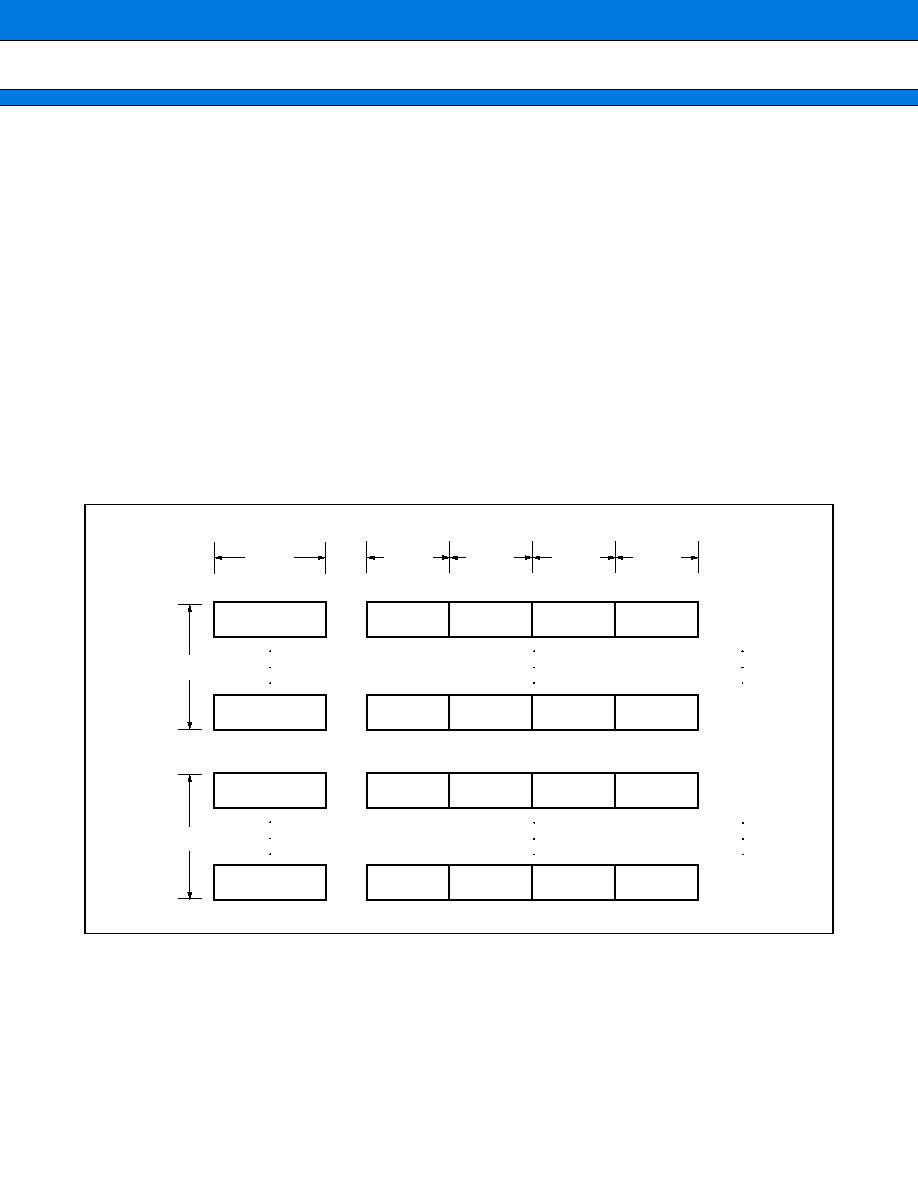
MB91360G Series
77
s
PERIPHERAL RESOURCES
1.
INSTRUCTION CACHE
This section describes the instruction cache memory included in FR50 Family members and it operation. This
only applies to MB91FV360GA.
(1) General Description
The instruction cache is temporary memory. When an external low-speed memory accesses an instruction code,
the instruction cache stores the single-accessed code to increase the second and subsequent access
speeds.Setting this memory to the RAM mode enables software to directly read and write instruction cache data
RAM and tag RAM.
(2) Main Body Structure
Instruction Cache Structure
∑ FR basic instruction length : 2 bytes
∑ Block arrangement system : 2-way set associative system
∑ Block
One way consists of 128 blocks.
One block consists of 16 bytes (
=
4 sub-blocks) .
One sub-block consists of 4 bytes (
=
1 bus access unit) .
4 bytes
4 bytes
4 bytes
4 bytes
4 bytes
I3
I2
I1
I0
Way 1
Way 2
Cache tag
Sub-block 3 Sub-block 2 Sub-block 1 Sub-block 0
Block 0
Sub-block 3 Sub-block 2 Sub-block 1 Sub-block 0
Block 127
Block 0
Block 127
Sub-block 3 Sub-block 2 Sub-block 1 Sub-block 0
Sub-block 3 Sub-block 2 Sub-block 1 Sub-block 0
Cache tag
Cache tag
Cache tag
128 blocks
128 blocks
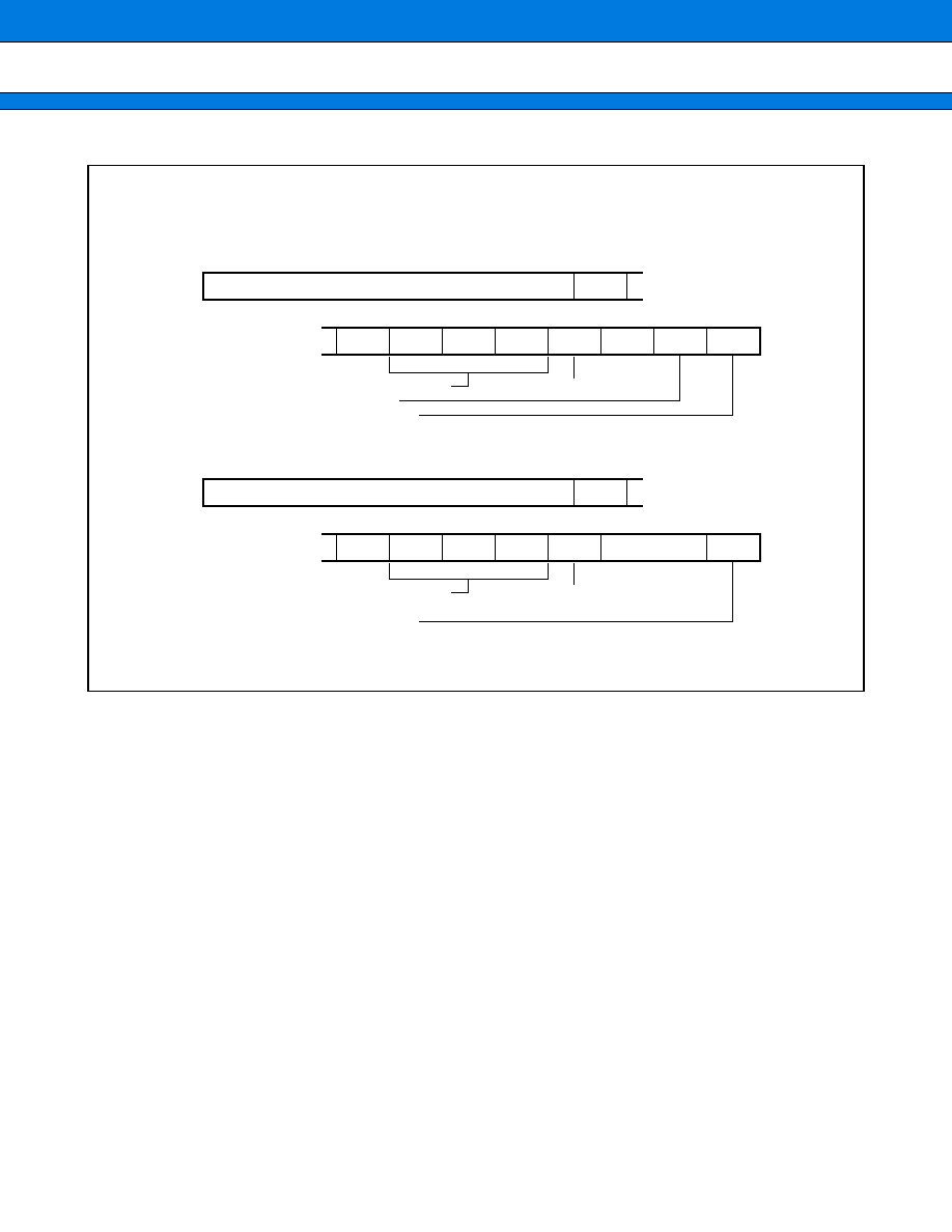
MB91360G Series
78
Instruction Cache Tag
07
06
05
04
03
02
01
00
SBV2
SBV3
ABV1
SBV0
TAGV
Reserved
LRU
ETLK
31
Way 1
09
08
Address tag
Reserved
TAG valid
Sub-block valid
LRU
Entry lock
07
06
05
04
03
02
01
00
SBV2
SBV3
ABV1
SBV0
TAGV
Reserved
ETLK
31
Way 2
09
08
Address tag
Reserved
TAG valid
Sub-block valid
Entry lock
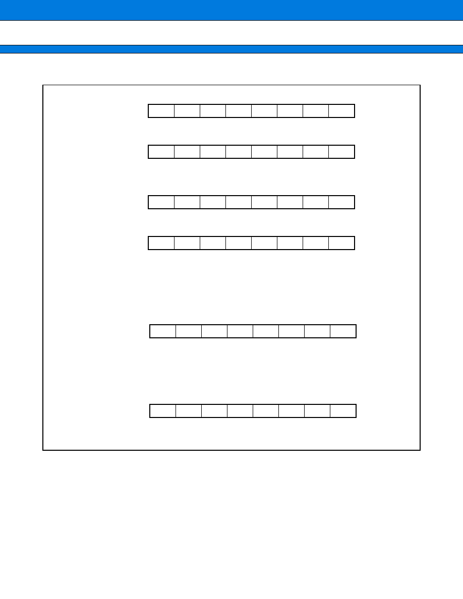
MB91360G Series
79
(3) Control Register Structure
IRBS [bits 15 to 12] These bits are used to set the base address of cache RAM at access in the RAM mode.
Align cache RAM in units of 4 K bytes. These bits are initialized by INIT. The initial value is the 00012000
H
address.
The ICHCR (I-CacHe Control Register) controls the instruction cache operations.
Writing to the ICHCR does not affect caching of instructions fetched within three subsequent cycles.
IRBS (32 bits)
Initial value
Address : 00000300
H
00000000
B
Initial value
00000001
B
ICR26
Initial value
Address : 00000302
H
0010 - - - -
B
Initial value
- - - - - - - -
B
ISIZE (8 bits)
Initial value
00000307
H
- - - - - - 11
B
ICHCR (8 bits)
Initial value
000003E7
H
0 - 000000
B
R
R
R
R
R
R
R
31
30
29
28
27
26
25
24
0
R
0
0
0
0
0
0
0
R
R
R
R
R
R
R
23
22
21
20
19
18
17
16
0
R
0
0
0
0
0
0
1
R/W
R/W
R/W
15
14
13
12
11
10
9
8
IRBS
R/W
IRBS
IRBS
IRBS
7
6
5
4
3
2
1
0
R/W
R/W
7
6
5
4
3
2
1
0
SIZE1
SIZE0
R/W
R/W
R/W
R/W
R/W
R/W
7
6
5
4
3
2
1
0
R/W
RAM
GBLK
ALFL
EOLK
ELKR
FLSH
ENAB

MB91360G Series
80
2.
BOOT ROM
The Boot ROM is a fixed start-up routine which is located at FF000 (Reset entry) and will therefore be executed
after every RST or INIT. The purpose of this ROM is to configure the device after a reset and to provide a simple
serial bootloader for programming the embedded Flash memories.
The Boot ROM contains three logical parts :
(1) Chip Initializations
Immediately after each reset, the following settings will be made :
CS0 : 200000...2FFFFF, 32 Bit Bus, 1 wait-state (default external access)
CS7 : 100000...10FFFF, 16 Bit Bus, 1 wait-state (CAN)
In addition, the Table-Base Register will be initialized to 1FFC00 (F361GA only) and the synchronous reset (see
TBCR) will be enabled.
(2) Check for Bootcondition
After the chip initialization, the "Security-Vector" will be checked (Vector #66) . The purpose of this feature is to
disable the bootstraploader due to security reasons.
The RSRR (reset cause register) will be read and saved. If no power-on reset (external INITX input, RSRR
=
0x80) is indicated, a branch to the user application will be initiated (Branch to 1F4000) .
If INITX was detected and the "Security-Vector" check okay, the following conditions must be met in order to
start the Bootstraploader :
Within a certain time, the start-up character "V" must be received via UART0 (9600, 8N1) . The time-out is set
to 200 ms.
(3) Bootstraploader
If the Bootcondition was met, an acknowledge character "F" will be transmitted via UART0 to indicate that the
Bootloader is ready to accept commands. 4 different commands are possible :
Receive and write to a specified memory block
Dump the contents of a specified memory block
Initiate a "CALL" to a certain location
Re-dump a calculated checksum for verification
(4) Configuration Register (F362Mode Register F362MD)
This register is used to control which pins of the external bus interface are active, where the pins for the external
DMA channel are located and which I
2
C module is used.
address
00001FE
H
access
Initial value
R/W
0
R/W
0
R/W
0
R/W
0
R/W
0
R/W
0
R/W
0
bit 15
bit 14
bit 13
bit 12
bit 11
bit 10
bit 9
bit 8
ASYMCLKT HIZ_D_A
HIZ_ECLK
HIZ_D_23_16 HIZ_D_15_0
DMASWP
IICSEL
ADRSWAP
R/W
0

MB91360G Series
81
3.
CLOCK MODULATOR
An important property of MCUs and other electronic devices is their electromagnetic compatibility - EMC. Besides
a low susceptibility against external interferences, a low radiated emission is desired to avoid interference of
adjacent devices.
Particularly the system clock and derived signals such as data- and address busses contribute significantly to
the radiated emission. The purpose of the clock modulator is to spread the energy of these signals over a wide
range of frequencies and thus reducing the amplitudes of the fundamental and harmonic frequencies.
With the use of an advanced frequency modulation algorithm, the Fujitsu built in clock modulator can achieve
an attenuation of up to 20-25 dB compared to non modulated clock operation. Since the modulator is highly
configurable, it can be optimally adjusted to the actual application in order to achieve minimal electromagnetic
interference.
By default, the modulator is disabled and the MCU is running with unmodulated clock.
If you plan to use this feature, please contact Fujitsu.

MB91360G Series
82
4.
I/O PORTS
The I
/
O port registers consist of the
"
port data registers
(
PDR
) ",
the
"
data direction registers
(
DDR
) "
and the
"
port function registers
(
PFR
) "
.
The bits in PDRs correspond to the bits in DDRs and PFRs. Similarly, the register bits correspond to the port pins.
The port data registers contain the port I/O data and the data direction registers specify whether the correspond-
ing bits (pins) are inputs or outputs. Bits set to "0" are inputs and bits set to "1" are outputs. The port function
registers specify whether the port is used as peripheral port or as "I/O" port. Usually bits set to "0" mean I/O port
and bits set to "1" mean functional port.
In case of analog peripherals there is additional circuitry to ensure that the digital logic is not disturbed by the
analog signals. If the analog input function e.g. ADC is enabled the digital input is fixed to "0".
∑ Input mode (DDR
=
"0")
PDR read : Reads the level on the corresponding external pin.
PDR write : writes the PDR setting value.
∑ Output mode (DDR
=
"1")
PDR read : Reads the PDR value.
PDR write : Outputs the PDR value to the corresponding external pins.
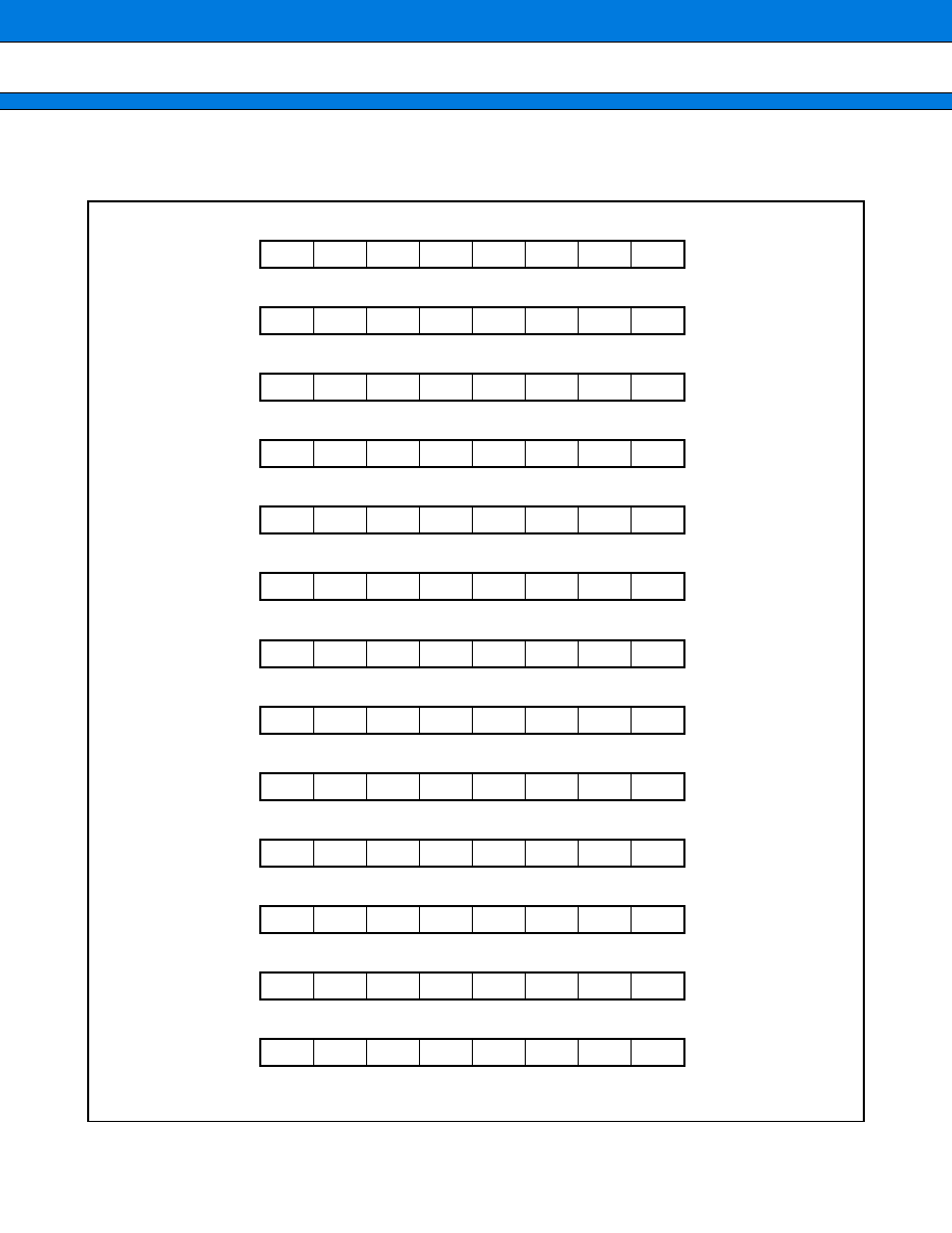
MB91360G Series
83
(1) Register configuration
Port Data Register
(Continued)
PDR7
Initial value
Access
Address : 00000007
H
1111XXXX
B
R/W
PDR8
Initial value
Access
Address : 00000008
H
XXXXXXXX
B
R/W
PDR9
Initial value
Access
Address : 00000009
H
XXXXXXX1
B
R/W
PDRB
Initial value
Access
Address : 0000000B
H
XXXXXXXX
B
R/W
PDRG
Initial value
Access
Address : 00000010
H
XXXXXXXX
B
R/W
PDRH
Initial value
Access
Address : 00000011
H
XXXXXXXX
B
R/W
PDRI
Initial value
Access
Address : 00000012
H
X - - - X - - -
B
R/W
PDRJ
Initial value
Access
Address : 00000013
H
XXXXXXXX
B
R/W
PDRK
Initial value
Access
Address : 00000014
H
XXXXXXXX
B
R/W
PDRL
Initial value
Access
Address : 00000015
H
XXXXXXXX
B
R/W
PDRM
Initial value
Access
Address : 00000016
H
- - - - XXXX
B
R/W
PDRN
Initial value
Access
Address : 00000017
H
- -XXXXXX
B
R/W
PDRO
Initial value
Access
Address : 00000018
H
XXXXXXXX
B
R/W
7
6
5
4
3
2
1
0
P76
P77
P75
P74
P73
P72
P71
P70
7
6
5
4
3
2
1
0
P86
P87
P85
P84
P83
P82
P81
P80
7
6
5
4
3
2
1
0
P96
P97
P95
P94
P93
P92
P91
P90
7
6
5
4
3
2
1
0
PB6
PB7
PB5
PB4
PB3
PB2
PB1
PB0
7
6
5
4
3
2
1
0
PG6
PG7
PG5
PG4
PG3
PG2
PG1
PG0
7
6
5
4
3
2
1
0
PG6
PG7
PG5
PG4
PG3
PG2
PG1
PG0
7
6
5
4
3
2
1
0
PH6
PH7
PH5
PH4
PH3
PH2
PH1
PH0
7
6
5
4
3
2
1
0
PI3
P17
7
6
5
4
3
2
1
0
PJ6
PJ7
PJ5
PJ4
PJ3
PJ2
PJ1
PJ0
7
6
5
4
3
2
1
0
PK6
PK7
PK5
PK4
PK3
PK2
PK1
PK0
7
6
5
4
3
2
1
0
PL6
PL7
PL5
PL4
PL3
PL2
PL1
PL0
7
6
5
4
3
2
1
0
PM3
PM2
PM1
PM0
7
6
5
4
3
2
1
0
PN5
PN4
PN3
PN2
PN1
PN0
7
6
5
4
3
2
1
0
PO6
PO7
PO5
PO4
PO3
PO2
PO1
PO0
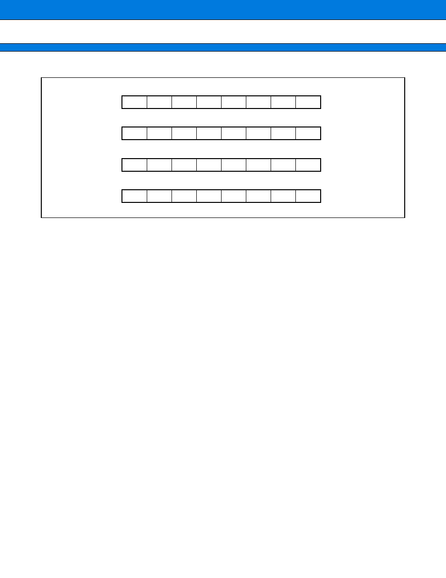
MB91360G Series
84
(Continued)
PDRP
Initial value
Access
Address : 00000019
H
XXXXXXXX
B
R/W
PDRQ
Initial value
Access
Address : 0000001A
H
--XXXXXX
B
R/W
PDRR
Initial value
Access
Address : 0000001B
H
XXXXXXXX
B
R/W
PDRS
Initial value
Access
Address : 0000001C
H
XXXXXXXX
B
R/W
7
6
5
4
3
2
1
0
PP6
PP7
PP5
PP4
PP3
PP2
PP1
PP0
7
6
5
4
3
2
1
0
PQ5
PQ4
PQ3
PQ2
PQ1
PQ0
7
6
5
4
3
2
1
0
PR6
PR7
PR5
PR4
PR3
PR2
PR1
PR0
7
6
5
4
3
2
1
0
PS6
PS7
PS5
PS4
PS3
PS2
PS1
PS0
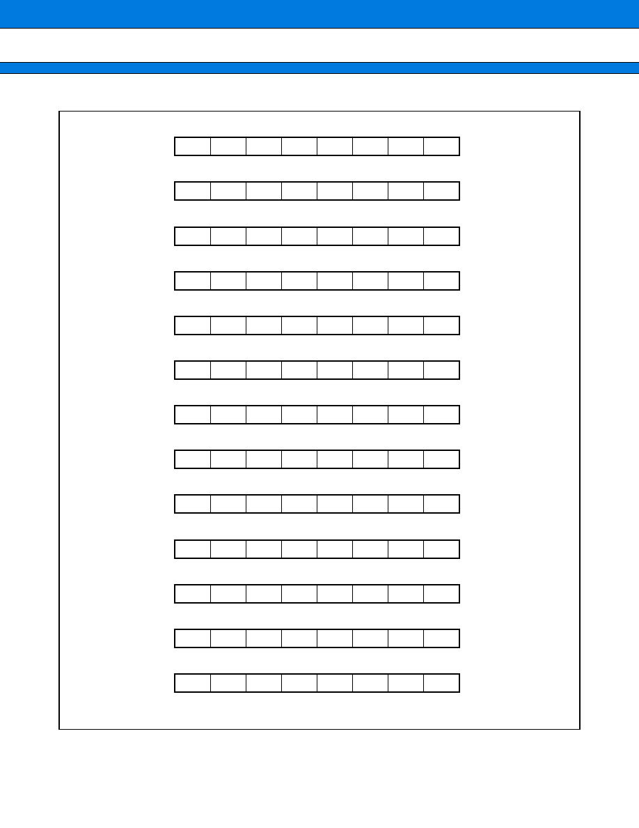
MB91360G Series
85
Data directon Register
(Continued)
DDR7
Initial value
Access
Address : 00000607
H
00000000
B
R/W
DDR8
Initial value
Access
Address : 00000608
H
00000000
B
R/W
DDR9
Initial value
Access
Address : 00000609
H
00000000
B
R/W
DDRB
Initial value
Access
Address : 0000600B
H
00000000
B
R/W
DDRG
Initial value
Access
Address : 00000400
H
00000000
B
R/W
DDRH
Initial value
Access
Address : 00000401
H
00000000
B
R/W
DDRI
Initial value
Access
Address : 00000402
H
- - - - 0 - - -
B
R/W
DDRJ
Initial value
Access
Address : 00000403
H
00000000
B
R/W
DDRK
Initial value
Access
Address : 00000404
H
00000000
B
R/W
DDRL
Initial value
Access
Address : 00000405
H
00000000
B
R/W
DDRM
Initial value
Access
Address : 00000406
H
- - - - 0000
B
R/W
DDRN
Initial value
Access
Address : 00000407
H
- -000000
B
R/W
DDRO
Initial value
Access
Address : 00000408
H
00000000
B
R/W
7
6
5
4
3
2
1
0
P76
P77
P75
P74
P73
P72
P71
P70
7
6
5
4
3
2
1
0
P86
P87
P85
P84
P83
P82
P81
P80
7
6
5
4
3
2
1
0
P96
P97
P95
P94
P93
P92
P91
P90
7
6
5
4
3
2
1
0
PB6
PB7
PB5
PB4
PB3
PB2
PB1
PB0
7
6
5
4
3
2
1
0
PG6
PG7
PG5
PG4
PG3
PG2
PG1
PG0
7
6
5
4
3
2
1
0
PG6
PG7
PG5
PG4
PG3
PG2
PG1
PG0
7
6
5
4
3
2
1
0
PH6
PH7
PH5
PH4
PH3
PH2
PH1
PH0
7
6
5
4
3
2
1
0
PI3
7
6
5
4
3
2
1
0
PJ6
PJ7
PJ5
PJ4
PJ3
PJ2
PJ1
PJ0
7
6
5
4
3
2
1
0
PK6
PK7
PK5
PK4
PK3
PK2
PK1
PK0
7
6
5
4
3
2
1
0
PL6
PL7
PL5
PL4
PL3
PL2
PL1
PL0
7
6
5
4
3
2
1
0
PM3
PM2
PM1
PM0
7
6
5
4
3
2
1
0
PN5
PN4
PN3
PN2
PN1
PN0
7
6
5
4
3
2
1
0
PO6
PO7
PO5
PO4
PO3
PO2
PO1
PO0

MB91360G Series
86
(Continued)
DDRP
Initial value
Access
Address : 00000409
H
00000000
B
R/W
DDRQ
Initial value
Access
Address : 0000040A
H
--000000
B
R/W
DDRR
Initial value
Access
Address : 0000040B
H
00000000
B
R/W
DDRS
Initial value
Access
Address : 0000040C
H
00000000
B
R/W
7
6
5
4
3
2
1
0
PP6
PP7
PP5
PP4
PP3
PP2
PP1
PP0
7
6
5
4
3
2
1
0
PQ5
PQ4
PQ3
PQ2
PQ1
PQ0
7
6
5
4
3
2
1
0
PR6
PR7
PR5
PR4
PR3
PR2
PR1
PR0
7
6
5
4
3
2
1
0
PS6
PS7
PS5
PS4
PS3
PS2
PS1
PS0
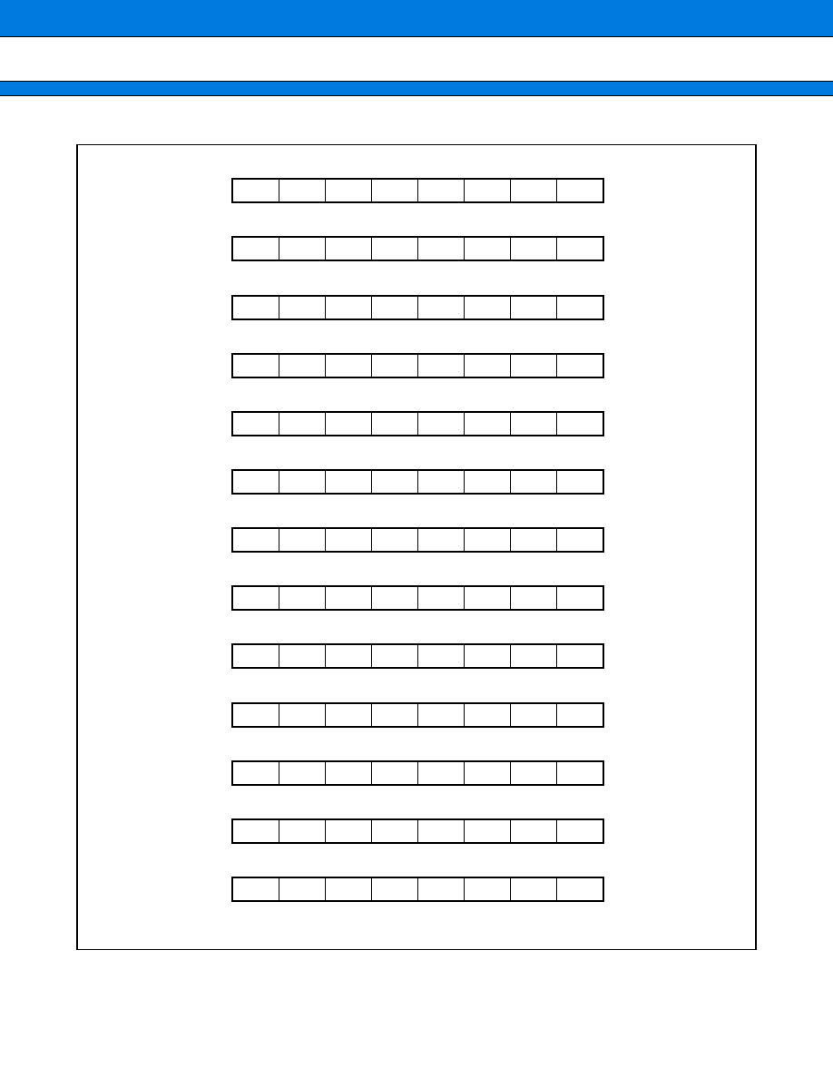
MB91360G Series
87
Port function registers (PFR)
(Continued)
PFR7
Initial value Access
Address : 00000617
H
00001111
B
R/W
PFR8
Initial value Access
Address : 00000618
H
111110 -
-
B
R/W
PFR9
Initial value Access
Address : 00000619
H
11110101
B
R/W
PFRB
Initial value Access
Address : 0000061B
H
00000000
B
R/W
PFR27
Initial value Access
Address : 00000627
H
1111 -
00 -
B
R/W
PFRG
Initial value Access
Address : 00000410
H
00000000
B
R/W
PFRH
Initial value Access
Address : 00000411
H
00000000
B
R/W
PFRI
Initial value Access
Address : 00000412
H
-
-
-
-
0 -
-
-
B
R/W
PFRJ
Initial value Access
Address : 00000413
H
00000000
B
R/W
PFRK
Initial value Access
Address : 00000414
H
00000000
B
R/W
PFRL
Initial value Access
Address : 00000415
H
00000000
B
R/W
PFRM
Initial value Access
Address : 00000416
H
- - - - 0000
B
R/W
PFRN
Initial value Access
Address : 00000417
H
- - 000000
B
R/W
7
6
5
4
3
2
1
0
P76
P77
P75
P74
P73
P72
P71
P70
7
6
5
4
3
2
1
0
P86
P87
P85
P84
P83
P82
7
6
5
4
3
2
1
0
P96
P97
P95
P94
P93
P92
P91
P90
7
6
5
4
3
2
1
0
PB6
PB7
PB5
PB4
PB3
PB2
PB1
PB0
7
6
5
4
3
2
1
0
P276
P277
P275
P274
P273
P272
P271
P270
7
6
5
4
3
2
1
0
PG6
PG7
PG5
PG4
PG3
PG2
PG1
PG0
7
6
5
4
3
2
1
0
PH6
PH7
PH5
PH4
PH3
PH2
PH1
PH0
7
6
5
4
3
2
1
0
PI3
7
6
5
4
3
2
1
0
PJ6
PJ7
PJ5
PJ4
PJ3
PJ2
PJ1
PJ0
7
6
5
4
3
2
1
0
PK6
PK7
PK5
PK4
PK3
PK2
PK1
PK0
7
6
5
4
3
2
1
0
PL6
PL7
PL5
PL4
PL3
PL2
PL1
PL0
7
6
5
4
3
2
1
0
PM3
PM2
PM1
PM0
7
6
5
4
3
2
1
0
PN5
PN4
PN3
PN2
PN1
PN0
MB91360G Series
88
(Continued)
PFRO
Initial value Access
Address : 00000418
H
00000000
B
R/W
PFRP
Initial value Access
Address : 00000419
H
00000000
B
R/W
PFRQ
Initial value Access
Address : 0000041A
H
- - 000000
B
R/W
PFRR
Initial value Access
Address : 0000041B
H
00000000
B
R/W
PFRS
Initial value Access
Address : 0000041C
H
00000000
B
R/W
7
6
5
4
3
2
1
0
PO6
PO7
PO5
PO4
PO3
PO2
PO1
PO0
7
6
5
4
3
2
1
0
PP6
PP7
PP5
PP4
PP3
PP2
PP1
PP0
7
6
5
4
3
2
1
0
PQ5
PQ4
PQ3
PQ2
PQ1
PQ0
7
6
5
4
3
2
1
0
PR6
PR7
PR5
PR4
PR3
PR2
PR1
PR0
7
6
5
4
3
2
1
0
PS6
PS7
PS5
PS4
PS3
PS2
PS1
PS0

MB91360G Series
89
5.
DMA CONTROLLER
(
DMAC
)
The DMAC module is used to implement direct memory access (DMA) transfer in FR50 series devices.
In a DMA transfer controlled by this module, various types of data can be transferred at high speed without
involving the CPU, thus increasing system performance.
(1) Hardware Configuration
The following are the main components of the DMAC module :
∑ Five independent DMA channels
∑ 5-channel independent access control circuit
∑ 32-bit address registers (Reload can be specified : Two registers for each channel.)
∑ 16-bit transfer count registers (Reload can be specified : One register for each channel.)
∑ 4-bit block count registers (One register for each channel)
∑ External transfer request input pins DREQ0, DREQ1, and DREQ2 (only channels 0, 1, and 2)
∑ External transfer request acceptance output pins DACK0, DACK1, and DACK2 (only channels 0, 1, and 2)
∑ DMA termination output pins DEOP0, DEOP1, and DEOP2 (only channels 0, 1, and 2)
∑ Two-cycle transfer
(2) Main Functions
The following are the main functions of data transfer performed by the module :
∑ Independent data transfer in multiple channels is enabled (5 channels) .
a : Priority (channel 0
>
channel 1
>
channel 2
>
channel 3
>
channel 4)
b : Priority can be alternated between channel 0 and channel 1.
c : DMAC start cause
∑
External-only pin input (edge detection/level detection channels 0 to 2 only)
∑
Internal peripheral request (interrupt request is shared, including external interrupts)
∑
Software request (register write)
d : Transfer mode
∑
Demand transfer, burst transfer, step transfer, block transfer
∑
Addressing mode 32-bit full address specification (increase, decrease, fixed)
(An address increment/decrement size of
-
255 to
+
255 can be specified.)
∑
Data types of byte, halfword, and word lengths
∑
Single-shot/reload selectable

MB91360G Series
90
(3) Registers Configuration
Channel 0 control/status register A
Channel 0 control/status register B
Channel 1 control/status register A
Channel 1 control/status register B
Channel 2 control/status register A
Channel 2 control/status register B
Channel 3 control/status register A
Channel 3 control/status register B
Channel 4 control/status register A
Channel 4 control/status register B
Overall control register
Channel 0 transfer source address register
Channel 0 transfer destination address register
Channel 1 transfer source address register
Channel 1 transfer destination address register
Channel 2 transfer source address register
Channel 2 transfer destination address register
Channel 3 transfer source address register
Channel 3 transfer destination address register
Channel 4 transfer source address register
Channel 4 transfer destination address register
0000200
H
0000204
H
0000208
H
000020C
H
0000210
H
0000214
H
0000218
H
000021C
H
0000220
H
0000224
H
0000240
H
0001000
H
0001004
H
0001008
H
000100C
H
0001010
H
0001014
H
0001018
H
000101C
H
0001020
H
0001028
H
DMACA0
DMACB0
DMACA1
DMACB1
DMACA2
DMACB2
DMACA3
DMACB3
DMACA4
DMACB4
D M A C R
DMASA0
DMADA0
DMASA1
DMADA1
DMASA2
DMADA2
DMASA3
DMADA3
DMASA4
DMADA4
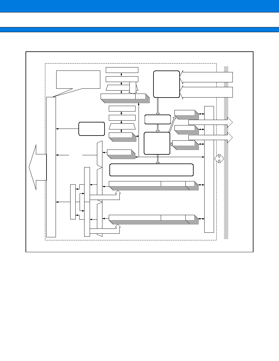
MB91360G Series
91
(4) Block Diagram
Read
Write
Read/Write
control
To
bus
controller
DMA trnasfer request
to bus controller
DDNO
Access
Address
Write-back
Write-back
Selector
Selector
Selector
Counter buffer
Counter buffer
Address counter
Bus control section
BLK register
DDNO register
DMA control
DTCR
Priority circuit
Status
transition
circuit
Counter
DMA start
cause selection
circuit and
request
acceptance
control
Write back
Buffer
Selector
Counter
Buffer
Selector
DTC 2-step register
DSS [3:0]
Peripheral start request/stop
External pin start request/stop
input
input
To transfer controller
Clear peripheral interrupt
Bus control section
ERIR, EDIR
TYPE, MOD, WS
IRQ [4:0]
MCLREQ
X-bus
DADM, DASZ [7:0] DADR
SDAM, SASZ [7:0] SADR
DSAD 2-step register
DDAD 2-step register
DMAC 5-channel block diagram

MB91360G Series
92
6.
UART
The UART is a serial I/O port for performing asynchronous (stop-start synchronization) communications.
The MB91360G series contains three UART channels.
(1) Features
∑ Full-duplex, double buffering
∑ Supports asynchronous (stop-start synchronization) communications
∑ Supports multi-processor mode
∑ Fully programmable baud rate
The baud rate can be set using an internal timer. (See the U-TIMER section.)
∑ Supports flexible baud rate setting using an external clock
∑ Error detection function (parity, framing, overrun)
∑ Non return to zero (NRZ) transfer signal
∑ Supports DMA transfer activation using an interrupt
MB91360G Series
93
(2) Register Configuration
Register structure
Serial input register (SIDR)
Serial output register (SODR)
Serial status register (SSR)
Serial mode register (SMR)
Serial control register (SCR)
UART level select register (ULS)
Address
Bits
Initial value
SMR
0000 0063
H
0000 006F
H
0000 007B
H
00
-
-
0
-
00
B
Access
Address
Bits
Initial value
SCR
0000 0062
H
0000 006E
H
0000 007A
H
00000100
B
Access
SIDR (R)/SODR (W)
SMR
SCR
R/W
R/W
Access
SSR
ULS
15
0
8 7
8 bits
8 bits
7
6
5
4
3
2
1
0
D6
D7
D5
D4
D3
D2
D1
D0
7
6
5
4
3
2
1
0
D6
D7
D5
D4
D3
D2
D1
D0
7
6
5
4
3
2
1
0
ORE
PE
FRE
RDRF
TDRE
RIE
TIE
7
6
5
4
3
2
1
0
MD0
MD1
CS0
SCKE
7
6
5
4
3
2
1
0
P
PEN
SBL
CL
A/D
REC
RXE
TXE
7
6
5
4
3
2
1
0
NSDO
NSDI
UTDBL
UDBL
R/W
W
7
6
5
4
3
2
1
0
MD2
R/W
MD1
Reserved Reserved
CS0
Reserved Reserved Reserved
R/W
R/W
R/W
R/W
W
R/W
R/W
7
6
5
4
3
2
1
0
P
R/W
PEN
SBL
CL
A/D
REC
RXE
TXE
MB91360G Series
94
(
3
)
Block Diagram
SI
MD1
MD0
CS0
SCKE
SOE
PEN
P
SBL
CL
A/D
REC
RXE
TXE
PE
ORE
FRE
RDRF
TDRE
RIE
TIE
R - BUS
SIDR
SODR
Control signals
Control signals
From U-TIMER
(Reception data)
Start bit detecter
Received bit
counter
Received parity
bit counter
Clock
selection
circuit
Reception status
detecton circuit
Reception error
occurrence
signal for DMA (to DMAC)
SMR
register
SCR
register
SSR
register
Receiving clock
Reception control
circuit
Reception
Shifter
Transmission
Shifter
SO
(Transmission data)
Reception
completed
Start of
transmission
Reception interrupt
(to CPU)
SCK (Clock)
Transmission
interrupt (to CPU)
Transmitting clock
Transmission
control circuit
Transmission
start circuit
Transmission
bit counter
Transmission
parity counter
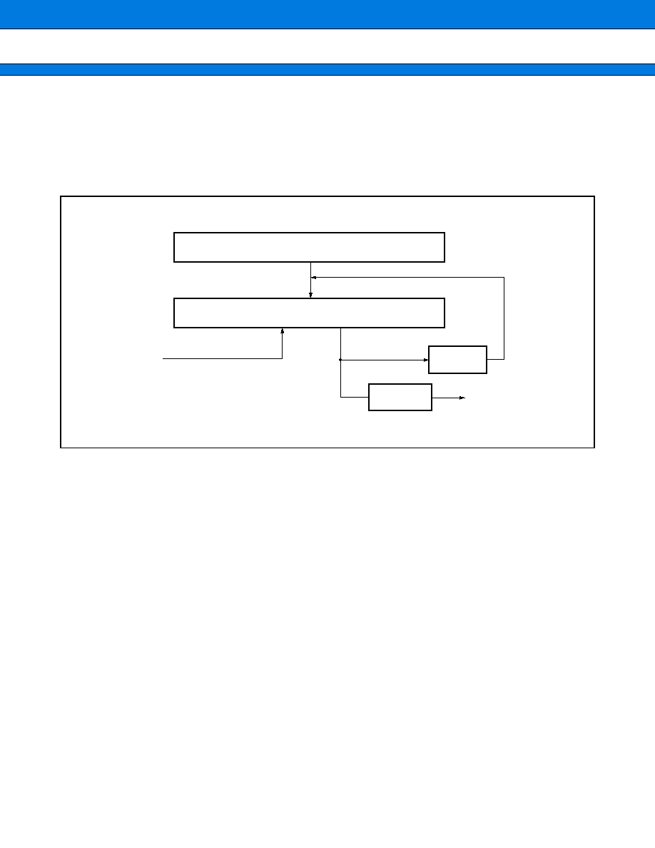
MB91360G Series
95
7.
U-TIMER (16-bit Timer for UART Baud Rate Generation)
The U-timer (U-TIMER) is a 16-bit timer used to generate the baud rate for the UART. The operating frequency
of the chip and the U-TIMER reload value can be combined to set a user-defined baud rate.
The MB91360G series contains three U-TIMER channels. The intervaltimers can count for a maximum of 216
◊
.
(
1
) Block Diagram
UTIMR (reload register)
UTIM (U-timer)
Clock
Load
Underflow
To UART
control
f.f.
15
15
(Peripheral clock)
0
0
MB91360G Series
96
(2) Register Configuration
Register structure
UTIMR Reload Register
UTIMC U Timer Control Register
UTIM
Address
Bits
Initial value Access
0-ch
1-ch
2-ch
00000068
H
00000074
H
00000080
H
0
R
UTIMR
Address
Bits
Initial value Access
0-ch
1-ch
2-ch
00000068
H
00000074
H
00000080
H
0
W
UTIMC
Address
Initial value Access
0-ch
1-ch
2-ch
0000006B
H
00000077
H
00000083
H
0---0001
R/W
UTIMR
UTIM
W
R/W
R
Access
R : Read,
W : Write
UTIMC
DRCL
15
0
8 7
15
14
2
1
0
b14
b15
b2
b1
b0
15
14
2
1
0
b14
b15
b2
b1
b0
7
6
5
4
3
2
1
0
UCC1
UNDR
Reserved
UTST
UTCR

MB91360G Series
97
8.
PWM TIMER
The PWM (Pulse Width Modulation) timer can output high-precision pulse waves at an arbitrary cycle and pulse
width (duty ratio) .
The MB91360G series contains eight PWM timer channels. Each of the channels consists of a 16-bit down-
counter, cycle setting register, duty setting register, and pin controller.
The control status register for each channel is used to indicate the operation status of the PWM timer. General
control registers 1 and 2 are common registers shared by four channels, serving for input and software triggering.
(1) Features
∑ The count clock for the 16-bit down-counter can be selected from among the following four types :
Internal clocks :
,
/4,
/16,
/64 (
: Machine clock for peripherals)
∑ The counter can be initialized to "FFFF
H
" by a reset or underflow.
The 16-bit down-counter causes an underflow when it changes from "0000
H
" to "FFFF
H
".
∑ Each channel has PWM outputs.
Eight channels : Eight output pins
∑ Registers
Cycle setting register : Data reload register with buffer
Data transfer from the buffer is performed either when an activation trigger is detected or when
the down-counter causes an underflow (cycle match) . The output is inverted at a cycle match.
Duty setting register : Compare register with buffer.
The value set in this register is compared to the counter value. The output is inverted when the values
match (duty match) .
∑ Pin control
A duty match causes a reset to "1" (given priority) .
An underflow causes a reset to "0".
The output value fix mode enables output of all "L" or all "H".
The polarity can also be specified.
∑ Interrupt requests can be generated by selecting the following interrupt sources :
Activation of the PWM timer (software trigger or trigger input)
Occurrence of an underflow (cycle match)
Occurrence of a duty match
Occurrence of an underflow (cycle match) or duty match
∑ You can set simultaneous activation of two or more channels using software or another interval timer. You can
also set restarting the PWM timer during operation.

MB91360G Series
98
(2) Register Configuration for Channels 0 to 3
GCN10
Bits
GCN20
PDBL0
PTMR
PCSR
PDUT
PCNH
PCNL
PTMR
PCSR
PDUT
PCNH
PCNL
PTMR
PCSR
PDUT
PCNH
R/W
R/W
R
W
W
R/W
R
W
W
R/W
R
W
W
R/W
15
PWM timer ch 0
PWM timer ch 1
PWM timer ch 2
PWM timer ch 3
7
Address
Access
Register name
0
8
0000011A
H
00000126
H
0000012E
H
00000136
H
PCNL
PTMR
PCSR
PDUT
PCNH
PCNL
R
W
W
R/W
General control register 10
Disable/General control register 20
ch0 timer register
ch0 cycle setting register
ch0 duty setting register
ch0 control status registers
ch1 timer register
ch1 cycle setting register
ch1 duty setting register
ch1 control status registers
ch2 timer register
ch2 cycle setting register
ch2 duty setting register
ch2 control status registers
ch3 timer register
ch3 cycle setting register
ch3 duty setting register
ch3 control status registers
0000013E
H
00000118
H
00000124
H
0000012C
H
00000134
H
0000013C
H
00000122
H
0000012A
H
00000132
H
0000013A
H
00000120
H
00000128
H
00000130
H
00000138
H
MB91360G Series
99
(3) PWM Timer Registers for Channels 4 to 7
GCN11
Bits
GCN21
PDBL1
PTMR
PCSR
PDUT
PCNH
PCNL
PTMR
PCSR
PDUT
PCNH
PCNL
PTMR
PCSR
PDUT
PCNH
R/W
R/W
R
W
W
R/W
R
W
W
R/W
R
W
W
R/W
15
PWM timer ch 4
PWM timer ch 5
PWM timer ch 6
PWM timer ch 7
7
Address
Access
Register name
0
8
0000011E
H
00000146
H
0000014E
H
00000156
H
PCNL
PTMR
PCSR
PDUT
PCNH
PCNL
R
W
W
R/W
General control register 11
Disable/General control register 21
ch4 timer register
ch4 cycle setting register
ch4 duty setting register
ch4 control status registers
ch5 timer register
ch5 cycle setting register
ch5 duty setting register
ch5 control status registers
ch6 timer register
ch6 cycle setting register
ch6 duty setting register
ch6 control status registers
ch7 timer register
ch7 cycle setting register
ch7 duty setting register
ch7 control status registers
0000015E
H
0000011C
H
00000144
H
0000014C
H
00000154
H
0000015C
H
00000142
H
0000014A
H
00000152
H
0000015A
H
00000140
H
00000148
H
00000150
H
00000158
H
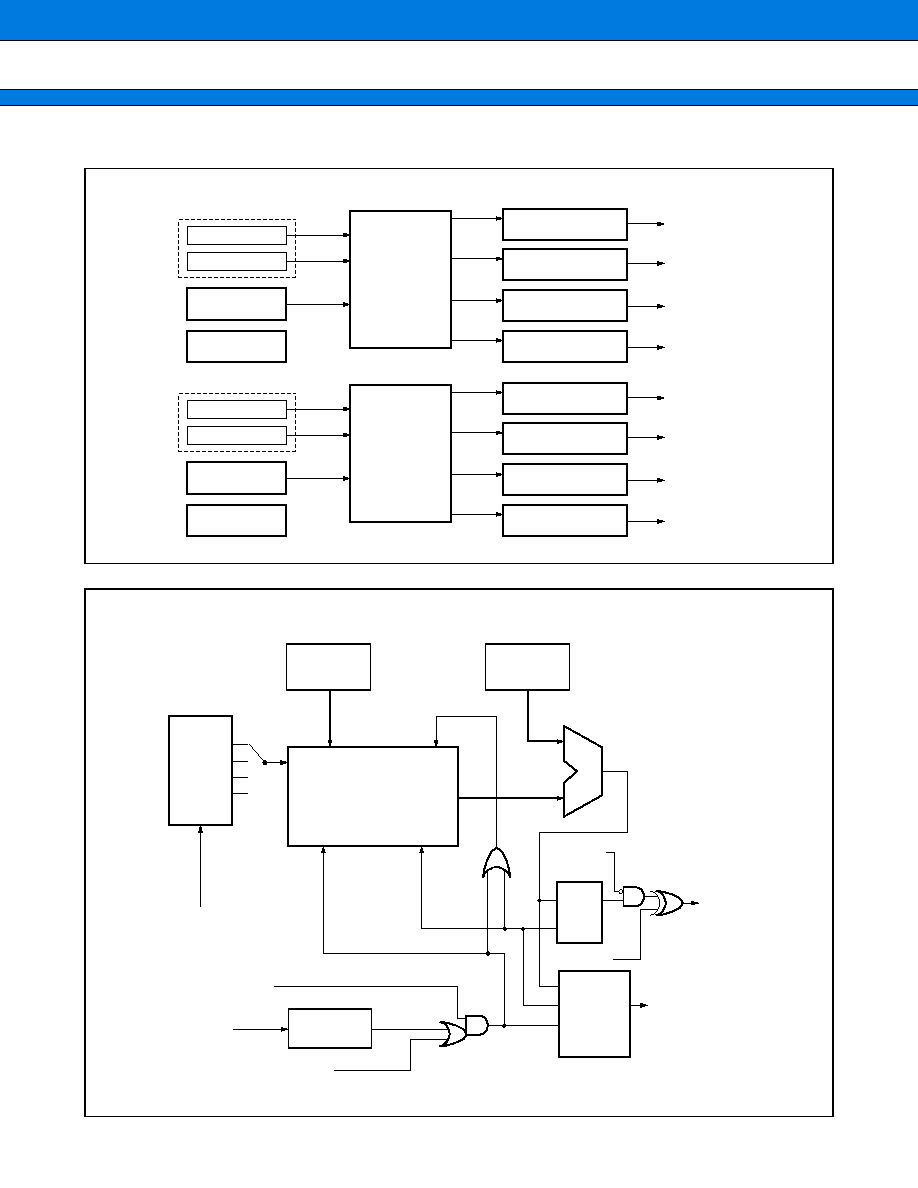
MB91360G Series
100
(4) Configuration Diagram of the Entire PWM Timer
(5) Configuration Diagram of PWM Timer 1 ch
OCPA0 (PWM0)
ch0
16-bit reload timer
General control
register 10
(source selection)
Output pins
ch1
General control
register 20
Disable
register 0
TRG input
PWM timer ch0
TRG input
PWM timer ch1
TRG input
PWM timer ch2
TRG input
PWM timer ch3
OCPA1 (PWM1)
OCPA2 (PWM2)
OCPA3 (PWM3)
OCPA4 (PWM4)
ch2
16-bit reload timer
General control
register 11
(source selection)
ch3
General control
register 21
Disable
register 1
TRG input
PWM timer ch4
TRG input
PWM timer ch5
TRG input
PWM timer ch6
TRG input
PWM timer ch7
OCPA5 (PWM5)
OCPA6 (PWM6)
OCPA7 (PWM7)
/ 1
/ 4
/ 16
/ 64
Clock
TRG input
(Internal trigger input)
PWM output
PCSR
PPG mask
Enable
Software trigger
Inverted bit
Load
PDUT
cmp
Interrupt
selection
Edge
detection
Start
Underflow
Prescalar
16-bit down-counter
Cycle setting register
Duty setting register
Peripheral clock (
)
S
R
Q
IRQ
(Interrupt request signal)
MB91360G Series
101
9.
16
-
BIT RELOAD TIMER
Each 16-bit reload timer consists of a 16-bit down-counter, a 16-bit reload register, a prescaler for generating
the internal count clock, and a control register.
The 16-bit reload timer can also activate DMA transfer using interrupts.
The MB91360G series contains six 16-bit reload timer channels.
(1) 16 bit Reloard Timer Register Configuration
Control status register (TMCSR)
16-bit timer register (TMR)
16-bit reload register (TMRLR)
15
14
13
12
11
10
9
8
CSL1
CSL0
7
6
5
4
3
2
1
0
RELD
INTE
UF
CNTE
TRG
15
0
15
0
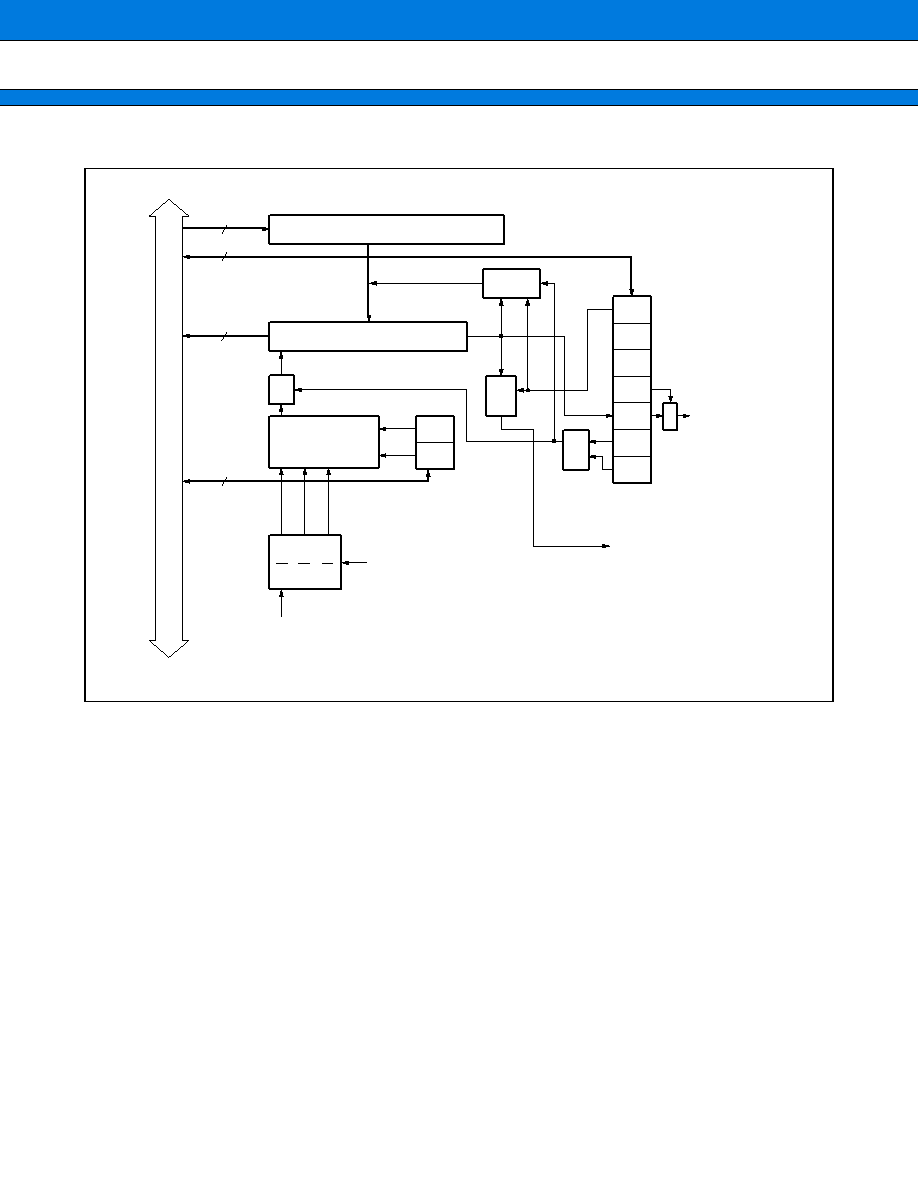
MB91360G Series
102
(2) Block diagram
RELD
INTE
UF
CNTE
TRG
OUT
CTL.
CSL1
CSL0
16
8
16
2
2
1
2
3
2
5
GATE
UF
IRQ
16-bit reload register
Reload
16-bit down-counter
Clock selector
R-BUS
Clear
prescalar
PWM (Reload timer 0-ch to 3-ch)*
A/D (Reaload timer 4-ch)*
* Internally connected
Internal clock

MB91360G Series
103
10. BIT SEARCH MODULE
The bit search module searches for a "0", "1", or change-point in the data written to the input register and returns
the position of the detected bit.
This section describes the data register for detecting zeros (BSD0) , data register for detecting ones (BSD1) ,
data register for detecting change-points (BSDC) , and detection result register (BSRR) .
a : Data register for detecting zeros (BSD0)
b : Date register for detecting ones (BSD1)
c : Data register for detecting change points (BSDC)
d : Detection Result Register (BSRR)
Address
Initial value
Access
0000 03F0
H
Indeterminate
W
Address
Initial value
Access
0000 03F4
H
Indeterminate
R/W
Address
Initial value
Access
0000 03F8
H
Indeterminate
W
Address
Initial value
Access
0000 03FC
H
Indeterminate
R
31
0
Register structure
31
0
Register structure
31
0
Register structure
31
0
Register structure
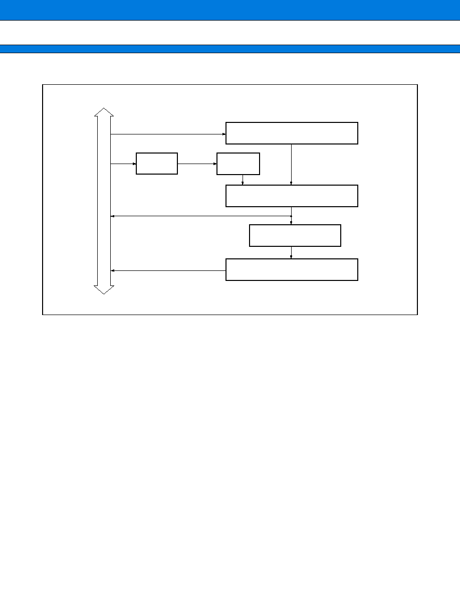
MB91360G Series
104
∑
∑
∑
∑
Block Diagram of the Bit Search Module
D-BUS
Input latch
Address
decoder
Detection
mode
One-detect data conversion
Bit search circuit
Search result

MB91360G Series
105
11.
10
-
BI
T A/D
CONVERTER
(
Successive Approximation Conversion Type
)
This section provides an overview of the A/D converter, describes the register structure and functions, and
describes the operation of the A/D converter.
A/D Converter converts analog input voltage into digital values, and provides the following features.
∑ Conversion time : minimum 178 cycles (32 MHz : 5.6
µ
s, 24 MHz : 7.4
µ
s, 16 MHz : 11.2
µ
s) per channel
∑ RC type successive approximation conversion with sample & hold circuit
∑ 10-bit resolution
∑ Program selection analog input from 16 channels
Single conversion mode : conversion of one selected channel
Scan conversion mode : continuous conversion of multiple channels, programmable for up to 16 channels
Single conversion mode : Convert the specified channel once only.
∑ Continuous mode : Repeatedly convert the specified channels.
∑ Stop mode : Convert one channel then temporarily halt until the next activation.
(Enables synchronization of the conversion start timing.)
∑ A/D conversion can be followed by an A/D conversion interrupt request to CPU. This interrupt, an option that
is ideal for continuous processing can be used to start a DMA transfer of the results of A/D conversion to
memory.
∑ Startup may be by software, external trigger (falling edge) or timer (rising edge)
MB91360G Series
106
Channel setting register (ADCH)
Mode register (ADMD)
Control status register (ADCS)
Data register (ADCD)
Disable register (ADBL)
bit
Address : 00009D
H
bit
Address : 00009C
H
bit
Address : 00009F
H
bit
Address : 0000A1
H
bit
Address : 0000A0
H
bit
Address : 0000A3
H
ADCS
ADCH
ADMD
ADBL
ADCD
15
0
8 7
8 bit
8 bit
7
6
5
4
3
2
1
0
ANS2
ANS3
ANS1
ANS0
ANE3
ANE2
ANE1
ANE0
15
14
13
12
11
10
9
8
MOD1
MOD0
STS1
STS0
7
6
5
4
3
2
1
0
INT
BUSY
INTE
PAUS
STRT
Reserved
7
6
5
4
3
2
1
0
D6
D7
D5
D4
D3
D2
D1
D0
15
14
13
12
11
10
9
8
D9
D8
15
14
13
12
11
10
9
8
DBL
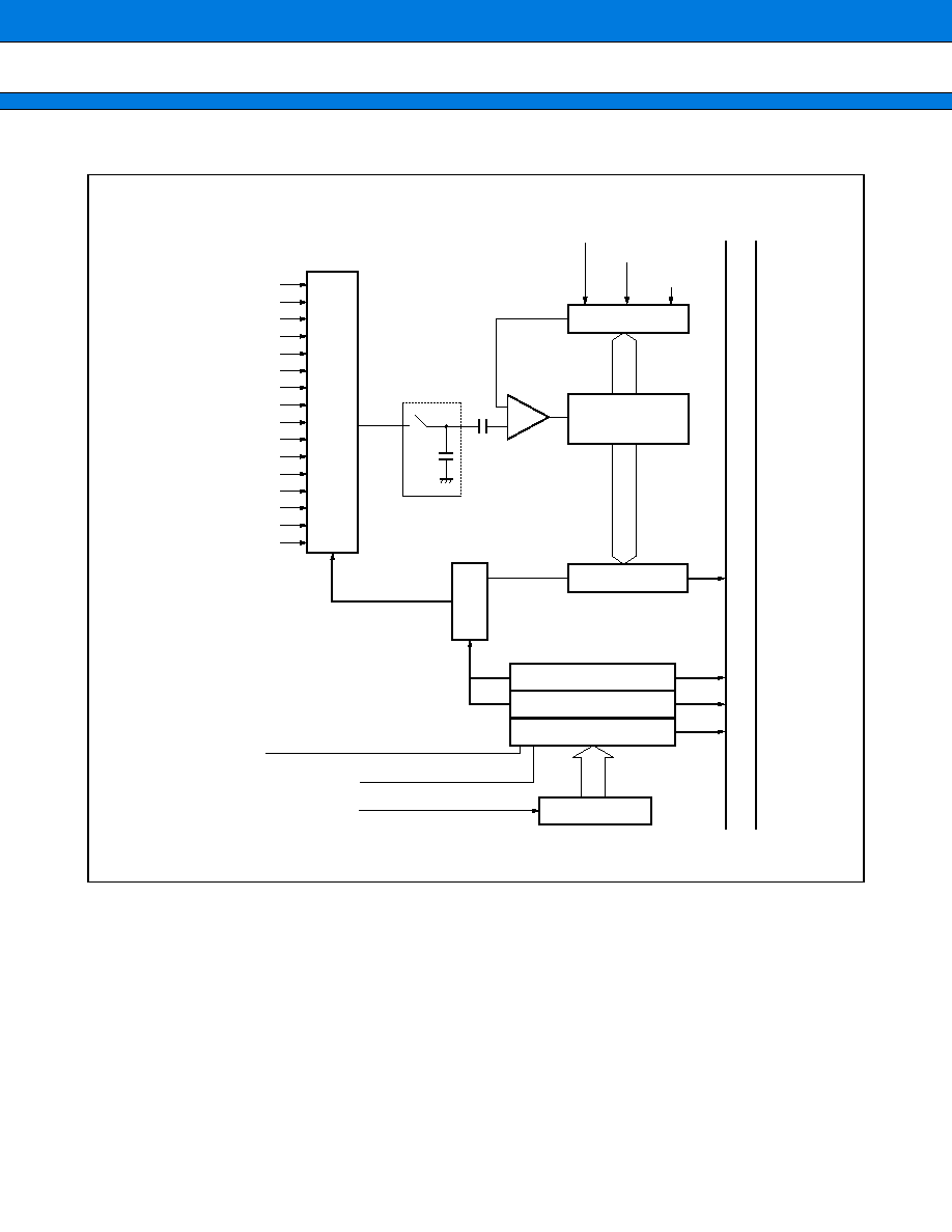
MB91360G Series
107
∑
∑
∑
∑
Block Diagram
MPX
D/A Converter
Sequential
comparison register
Sample-and-hold circuit
Comparator
Input circuit
ATGX
Decoder
AN0
AN1
AN2
AN3
AN4
AN5
AN6
AN7
AN8
AN9
ANA
ANB
ANC
AND
ANE
ANF
ADCD
Data bus
A/D data register
A/D channel setting register
A/D mode register
A/D control status register
Prescaler
ADCH
ADMD
ADCS
Operating clock
AV
CC
AV
RH
/AV
RL
AV
SS
Trigger activation
Machine clock (
)
Timer activation
Output of 16-bit reload timer 4
(internal connection)

MB91360G Series
108
12. INTERRUPT CONTROLLER
An interrupt controller controls interrupt acceptance and arbitration processing.
Hardware configuration
This module consists of the following :
∑
ICR register
∑
Interrupt priority evaluation circuit
∑
Interrupt level and interrupt number (vector) generator
∑
Hold request cancel request generator
Major functions
This module has the following major functions :
∑
Detecting an NMI request or interrupt request
∑
Priority evaluation (using the level or number)
∑
Transferring the level of the interrupt cause in the evaluation result (to the CPU)
∑
Transferring the number of the interrupt cause in the evaluation result (to the CPU)
∑
Instructing recovery from stop mode due to an NMI or interrupt level other than 11111 (to the CPU)
∑
Generating a hold request cancel request for the bus master
MB91360G Series
109
(1) Register Configuration
(Continued)
Address :
Address :
Address :
Address :
Address :
Address :
Address :
Address :
Address :
Address :
Address :
Address :
Address :
Address :
Address :
Address :
Address :
Address :
Address :
Address :
Address :
Address :
Address :
Address :
Address :
Address :
Address :
Address :
Address :
Address :
Address :
Address :
bit 7
6
5
4
3
2
1
0
ICR4
ICR3
ICR2
ICR1
ICR0
ICR4
ICR3
ICR2
ICR1
ICR0
ICR4
ICR3
ICR2
ICR1
ICR0
ICR4
ICR3
ICR2
ICR1
ICR0
ICR4
ICR3
ICR2
ICR1
ICR0
ICR4
ICR3
ICR2
ICR1
ICR0
ICR4
ICR3
ICR2
ICR1
ICR0
ICR4
ICR3
ICR2
ICR1
ICR0
ICR4
ICR3
ICR2
ICR1
ICR0
ICR4
ICR3
ICR2
ICR1
ICR0
ICR4
ICR3
ICR2
ICR1
ICR0
ICR4
ICR3
ICR2
ICR1
ICR0
ICR4
ICR3
ICR2
ICR1
ICR0
ICR4
ICR3
ICR2
ICR1
ICR0
ICR4
ICR3
ICR2
ICR1
ICR0
ICR4
ICR3
ICR2
ICR1
ICR0
ICR4
ICR3
ICR2
ICR1
ICR0
ICR4
ICR3
ICR2
ICR1
ICR0
ICR4
ICR3
ICR2
ICR1
ICR0
ICR4
ICR3
ICR2
ICR1
ICR0
ICR4
ICR3
ICR2
ICR1
ICR0
ICR4
ICR3
ICR2
ICR1
ICR0
ICR4
ICR3
ICR2
ICR1
ICR0
ICR4
ICR3
ICR2
ICR1
ICR0
ICR4
ICR3
ICR2
ICR1
ICR0
ICR4
ICR3
ICR2
ICR1
ICR0
ICR4
ICR3
ICR2
ICR1
ICR0
ICR4
ICR3
ICR2
ICR1
ICR0
ICR4
ICR3
ICR2
ICR1
ICR0
ICR4
ICR3
ICR2
ICR1
ICR0
ICR4
ICR3
ICR2
ICR1
ICR0
ICR4
ICR3
ICR2
ICR1
ICR0
ICR00
ICR01
ICR02
ICR03
ICR04
ICR05
ICR06
ICR07
ICR08
ICR09
ICR10
ICR11
ICR12
ICR13
ICR14
ICR15
ICR16
ICR17
ICR18
ICR19
ICR20
ICR21
ICR22
ICR23
ICR24
ICR25
ICR26
ICR27
ICR28
ICR29
ICR30
ICR31
00000440
H
00000441
H
00000442
H
00000443
H
00000444
H
00000445
H
00000446
H
00000447
H
00000448
H
00000449
H
0000044A
H
0000044B
H
0000044C
H
0000044D
H
0000044E
H
0000044F
H
00000450
H
00000451
H
00000452
H
00000453
H
00000454
H
00000455
H
00000456
H
00000457
H
00000458
H
00000459
H
0000045A
H
0000045B
H
0000045C
H
0000045D
H
0000045E
H
0000045F
H
R
R/W
R/W
R/W
R/W
MB91360G Series
110
(Continued)
Address :
Address :
Address :
Address :
Address :
Address :
Address :
Address :
Address :
Address :
Address :
Address :
Address :
Address :
Address :
Address :
Address :
bit 7
6
5
4
3
2
1
0
ICR4
ICR3
ICR2
ICR1
ICR0
ICR4
ICR3
ICR2
ICR1
ICR0
ICR4
ICR3
ICR2
ICR1
ICR0
ICR4
ICR3
ICR2
ICR1
ICR0
ICR4
ICR3
ICR2
ICR1
ICR0
ICR4
ICR3
ICR2
ICR1
ICR0
ICR4
ICR3
ICR2
ICR1
ICR0
ICR4
ICR3
ICR2
ICR1
ICR0
ICR4
ICR3
ICR2
ICR1
ICR0
ICR4
ICR3
ICR2
ICR1
ICR0
ICR4
ICR3
ICR2
ICR1
ICR0
ICR4
ICR3
ICR2
ICR1
ICR0
ICR4
ICR3
ICR2
ICR1
ICR0
ICR4
ICR3
ICR2
ICR1
ICR0
ICR4
ICR3
ICR2
ICR1
ICR0
ICR4
ICR3
ICR2
ICR1
ICR0
R
R/W
R/W
R/W
R/W
MHALTI
LVL4
LVL3
LVL2
LVL1
LVL0
R
R/W
R/W
R/W
R/W
R/W
ICR32
ICR33
ICR34
ICR35
ICR36
ICR37
ICR38
ICR39
ICR40
ICR41
ICR42
ICR43
ICR44
ICR45
ICR46
ICR47
HRCL
00000460
H
00000461
H
00000462
H
00000463
H
00000464
H
00000465
H
00000466
H
00000467
H
00000468
H
00000469
H
0000046A
H
0000046B
H
0000046C
H
0000046D
H
0000046E
H
0000046F
H
00000045
H
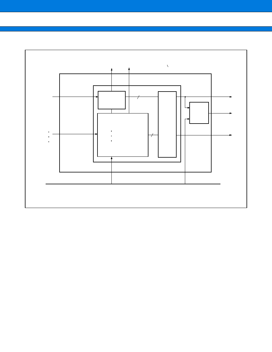
MB91360G Series
111
(2) Block Diagram
R100
R147
(DLYIRQ)
5
6
LEVEL4 to 0
MHALT1
VCT5 to 0
R-BUS
UNMI
WAKEUP (1 if LEVEL = 11111)
Priority evaluation
LEVEL evaluation
NMI
processing
ICR00
VECTOR
evaluation
LEVEL
and
VECTOR
generation
HLDREQ
withdrawal
request
ICR47
NMIRQ
(NMI request)
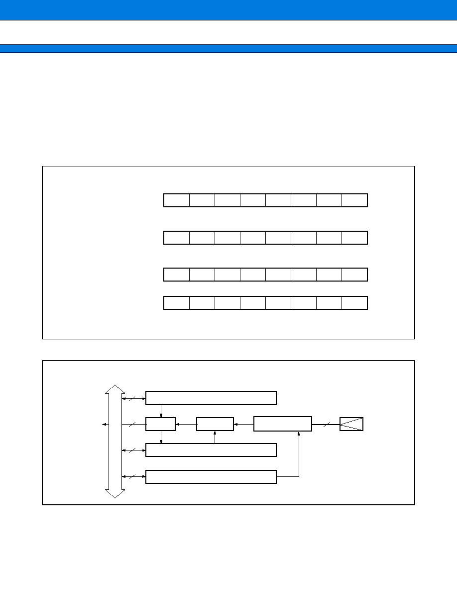
MB91360G Series
112
13. EXTERNAL INTERRUPT/NMI CONTROL BLOCK
The external interrupt/NMI controller controls external interrupt requests input from the NMI and INT0 to INT7
pins.
Detection of "H" levels, "L" levels, rising edges, or falling edges can be selected (except for the NMI) .
The external interrupt/NMI controller can also be used for DMA requests.
This section lists the registers of the controller and provides its block diagram.
(1) Register configuration of the External Interrupt NMI Controller
(2) Block diagram
External interruption permission register (ENIR)
External interruption factors register (EIRR)
Request level setting register (ELVR)
Bit
Bit
Bit
Bit
7
6
5
4
3
2
1
0
EN6
EN7
EN5
EN4
EN3
EN2
EN1
EN0
15
14
13
12
11
10
9
8
ER6
ER7
ER5
ER4
ER3
ER2
ER1
ER0
15
14
13
12
11
10
9
8
LA7
LB7
LB6
LA6
LB5
LA5
LB4
LA4
7
6
5
4
3
2
1
0
LA3
LB3
LB2
LA2
LB1
LA1
LB0
LA0
9
9
INT0 to 7
NMIX
8
8
8
R bus
Interrupt request
Enable interrupt request register
Gate
Request F/F
Edge detect
circuit
External interrupt request register
External level register
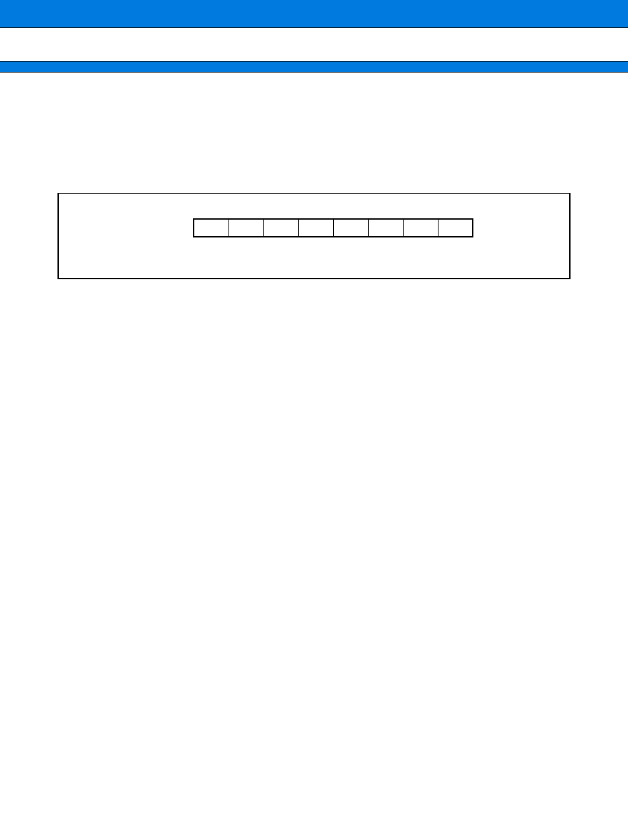
MB91360G Series
113
14. DELAYED INTERRUPT
Delayed Interrupt Control Register (DICR)
The delayed interrupt control register (DICR) is a delayed interrupt generator register and is used to generate
the task switching interrupt.
Structure of the DICR
Address
Bits
Initial value
00000044
H
- - - - - - - 0
Access
R/W
7
6
5
4
3
2
1
0
DLYI
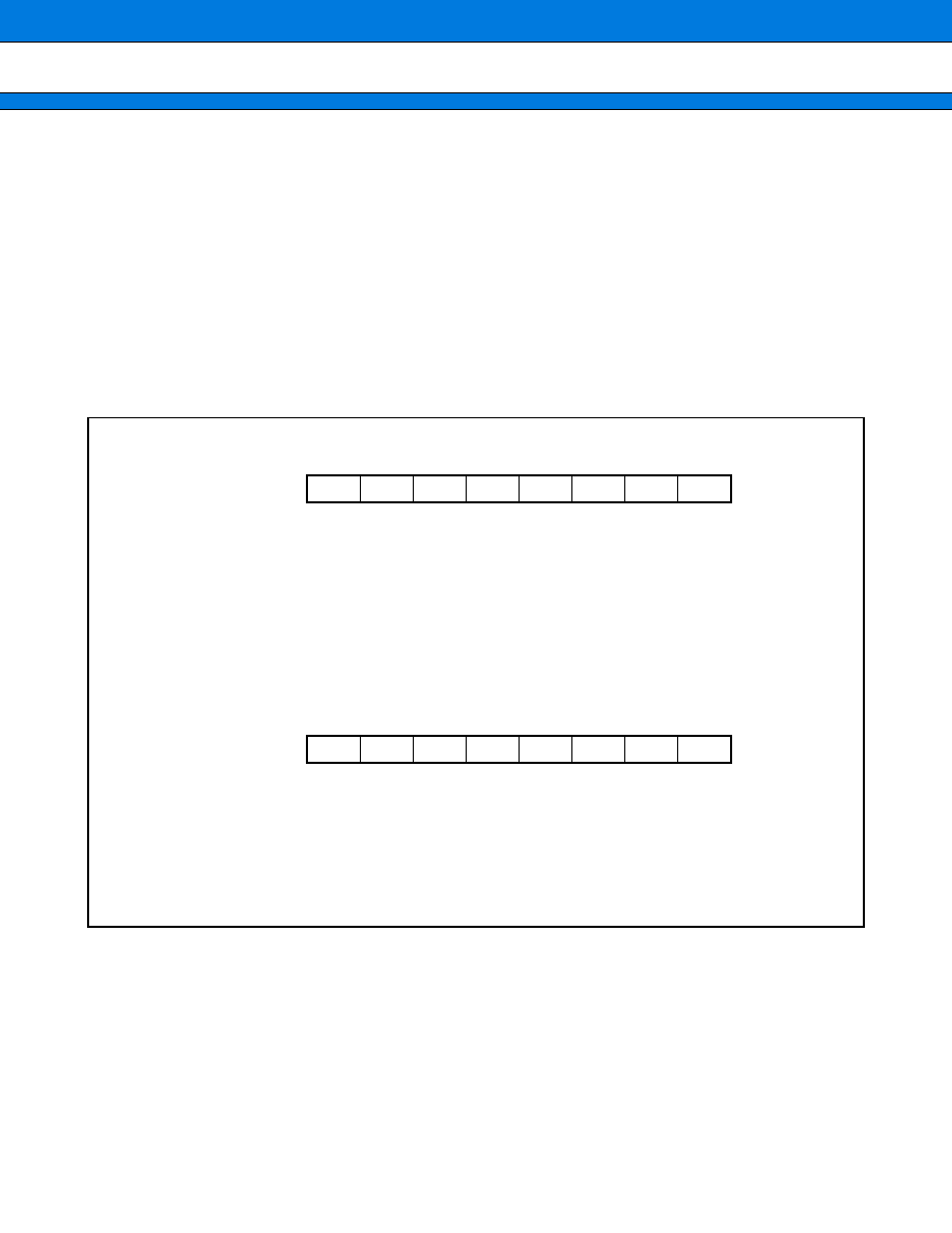
MB91360G Series
114
15. CLOCK GENERATION
The MB91V360 generates internal operating clocks as follows :
∑
Base clock generation : Device scales clock source input by 2 (X clock) or oscillates base clock with PLL to
generate basic clock (PLL clock)
∑
Generation of each internal clock : Device scales base clock to generate clocks supplied to each block
Generation and control of each clock are explained below.
Some devices allow the operation of the RTC module based on a separate 32 kHz subclock. See the section
about subclock operation for more details.
(1) Register Configuration
(Continued)
RSRR : Reset Source Register, Watchdog Timer Control Register
* : varies with reset factor
x : not initialized
** : After execution of the program in the internal boot ROM the reset source is visible
STCR
:
Standby Control Register
* : Valid only when this initialization is performed simultaneously with initialization by INITX : others same as INIT.
bit
address : 00000480
H
access
Initial Value (INITX)
Initial Value (INIT)
Initial Value (RST)
After Boot ROM **
bit
address : 00000481
H
access
Initial Value (INITX)
Initial Value (HSTX) *
Initial Value (INIT)
Initial Value (RST)
R
0
*
X
0
R
0
*
X
0
R
0
X
*
0
R
0
X
*
0
0
R/W
0
0
0
0
R/W
0
0
0
0
15
14
13
12
11
10
9
8
HSTB
R
1
*
X
0
INIT
WDOG
ERST
SRST
WT1
WT0
R/W
0
0
0
0
R/W
1
1
1
X
R/W
1
1
1
1
R/W
0
1
X
X
R/W
0
1
X
X
R/W
1
1
1
X
R/W
1
1
1
X
7
6
5
4
3
2
1
0
SLEEP
R/W
0
0
0
0
STOP
HIZ
SRST
OS1
OS0
OSCD2 OSCD1
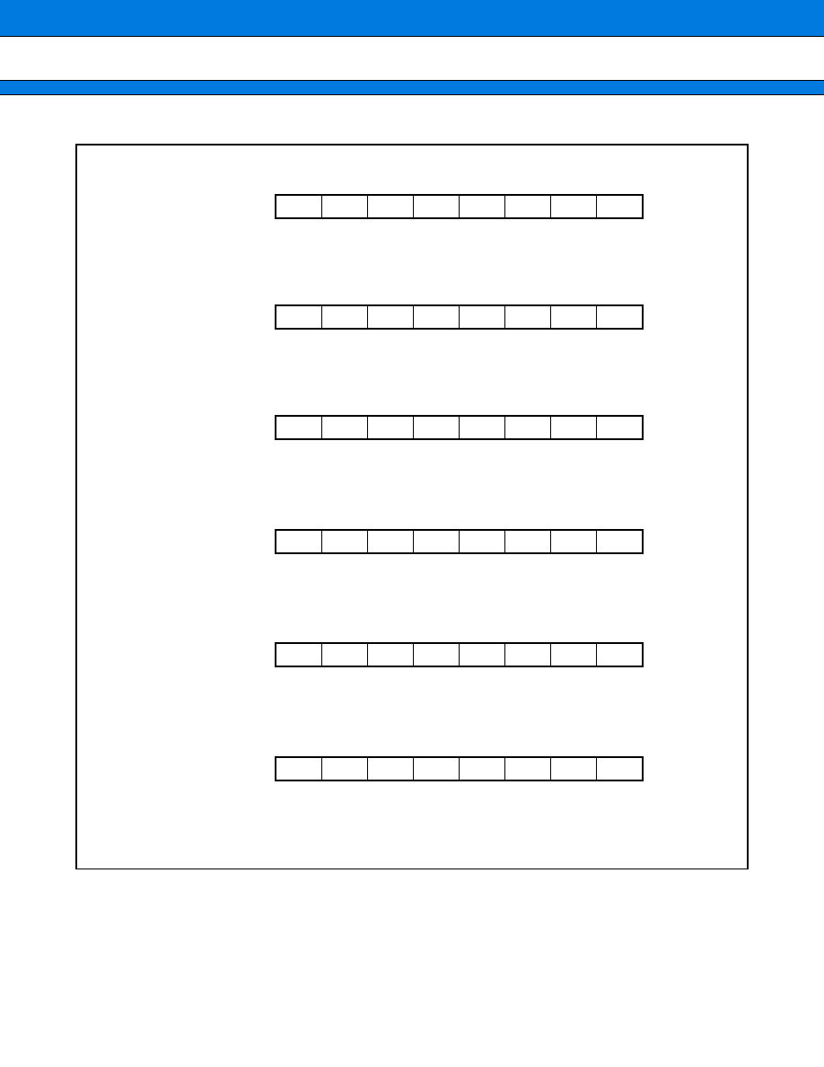
MB91360G Series
115
(Continued)
TBCR : Time-based counter control register
CTBR : Time-based counter clear register
CLKR : Clock source control register
WPR Watchdog reset generation postponement register
DIVR0 : Base clock division setting register 0
DIVR1 : Base clock division setting register 1
bit
address : 00000482
H
Initial Value (INIT)
Initial Value (RST)
bit
address : 00000483
H
Initial Value (INIT)
Initial Value (RST)
bit
address : 00000484
H
Initial Value (INIT)
Initial Value (RST)
bit
address : 00000485
H
Initial Value (INIT)
Initial Value (RST)
bit
address : 00000486
H
Initial Value (INIT)
Initial Value (RST)
bit
address : 00000487
H
Initial Value (INIT)
Initial Value (RST)
0
0
R/W
X
X
R/W
X
X
R/W
X
X
R/W
X
X
R/W
0
X
R/W
0
X
R/W
15
14
13
12
11
10
9
8
TBIE
0
0
R/W
TBIF
TBC2
TBC1
TBC0
SYNCR SYNCS
X
X
W
X
X
W
X
X
W
X
X
W
X
X
W
X
X
W
X
X
W
7
6
5
4
3
2
1
0
D6
X
X
W
D7
D5
D4
D3
D2
D1
D0
R/W
0
X
R/W
0
X
R/W
0
X
R/W
0
X
R/W
0
X
R/W
0
X
R/W
0
X
15
14
13
12
11
10
9
8
PLL1S2
R/W
0
X
PLL2S0
PLL1S1 PLL1S0 PLL2EN PLL1EN CLKS1
CLKS0
R/W
X
X
R/W
X
X
R/W
X
X
R/W
X
X
R/W
X
X
R/W
X
X
R/W
X
X
7
6
5
4
3
2
1
0
D6
R/W
X
X
D7
D5
D4
D3
D2
D1
D0
R/W
0
X
R/W
0
X
R/W
0
X
R/W
0
X
R/W
0
X
R/W
1
X
R/W
1
X
7
6
5
4
3
2
1
0
B2
R/W
0
X
B3
B1
B0
P3
P2
P1
P0
R/W
0
X
R/W
0
X
R/W
0
X
R/W
0
X
R/W
0
X
R/W
0
X
R/W
0
X
7
6
5
4
3
2
1
0
T2
R/W
0
X
T3
T1
T0
S3
S2
S1
S0
MB91360G Series
116
(Continued)
CMCR : Clock Control for CAN Modules
Subclock RTC32 (CLKR2)
This register is used to control the RTC32 mode bit for use in subclock system.
address
initial
0164
H
11111111
address
initial
0165
H
00000000
address
000046
H
access
initial value
bit 15
bit 14
bit 13
bit 12
bit 11
bit 10
bit 9
bit 8
PRE6
PRE7
PRE5
PRE4
PRE3
PRE2
PRE1
PRE0
bit 7
bit 6
bit 5
bit 4
bit 3
bit 2
bit 1
bit 0
PRES
R/W
0
R/W
0
R/W
0
bit 15
bit 14
bit 13
bit 12
bit 11
bit 10
bit 9
bit 8
RTC32
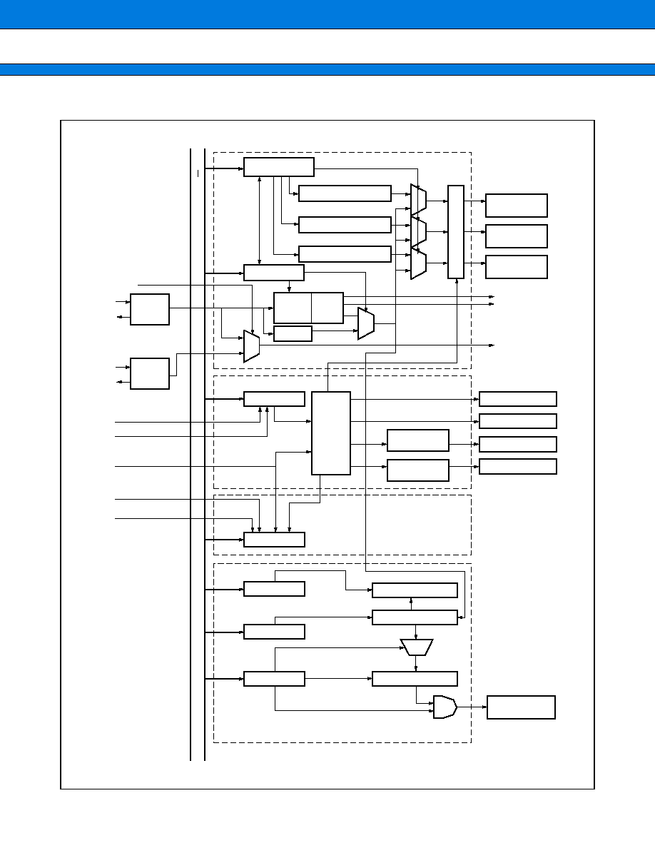
MB91360G Series
117
(2) Block Diagram
R
B
U
S
SELCLK
X0
X1
X0A
X1A
Oscillator
circuit
4 MHz
Oscillator
circuit
32 kHz
internal Interrrupt
internal Reset
HSTX
RSTX
INITX
DIVR0 and DIVR1
registers
[Clock generation block]
Stop control
CPU clock
CLKB
Ext. bus clock
CLKT
Resource clock
CLKP
MONCLK
Clock for RTC
Clock for CAN
CANCLK
Internal reset (RST)
Sleep state
Stop state
Internal reset (INIT)
CPU clock division
Resource clock division
Ext. bus clock division
CLKR register
PLL1
1/2
Clock
mod
1
0
[Stop/sleep control block]
Reset
occurrence F/F
Reset
occurrence F/F
STCR register
State
transition
control
circuit
RSRR register
[Reset source circuit]
WPR register
CTBR register
TBCR register
Watchdog F/F
Timer-base counter
Overflow detect. F/F
[Watchdog control block]
Time-base timer
interrupt request
Interrupt enable
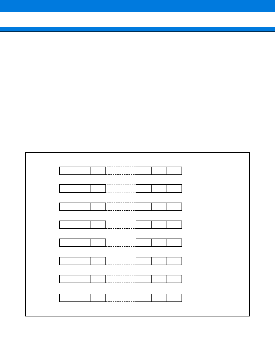
MB91360G Series
118
16. BUS INTERFACE
The external bus interface controls the interfaces with the external memory and external I/Os.
∑ Up to 32-bit (4 GB) address output.
∑ Up to eight independent banks provided by chip-select function
The banks can be set in 64-KB (minimum) at any position in the logic address space.
Can be set to no area
∑ 32/16/8 bit bus width setup can be performed for each chip-select area.
∑ Programmable automatic memory wait (up to 7 cycles) insertion
∑ Unused address/data pins can be used as I/O ports. (But see notes below)
Note : Chip Select Area CS7 is used for the internal CAN modules. The necessary register settings are done by
an internal boot routine. Take care not to overwrite register bits related to this CS area.
If the CAN macros which are connected internally to the external bus (also called User Logic Bus) are used,
a certain number of data, address and control ports of the external bus interface cannot be configured as
general purpose IO ports.
(1) Register Configuration
(Continued)
Area select Registers (ASR0 to ASR7)
After execution of the code in the initial boot ROM ASR0 is set to "0x20", and ASR7 to "0x10".
ASR0
Initial value
Access
INIT
RST
00000640
H
0000
H
0000
H
W
ASR1
Initial value
Access
INIT
RST
00000644
H
0000
H
XXXX
H
W
ASR2
Initial value
Access
INIT
RST
00000648
H
0000
H
XXXX
H
W
ASR3
Initial value
Access
INIT
RST
0000064C
H
0000
H
XXXX
H
W
ASR4
Initial value
Access
INIT
RST
0000650
H
0000
H
XXXX
H
W
ASR5
Initial value
Access
INIT
RST
00000654
H
0000
H
XXXX
H
W
ASR6
Initial value
Access
INIT
RST
00000658
H
0000
H
XXXX
H
W
ASR7
Initial value
Access
INIT
RST
0000065C
H
0000
H
XXXX
H
W
15
14
13
12
2
1
0
A30
A31
A29
PO4
PO3
A18
A17
A16
. . .
. . .
. . .
15
14
13
12
2
1
0
A30
A31
A29
PO4
PO3
A18
A17
A16
. . .
. . .
. . .
15
14
13
12
2
1
0
A30
A31
A29
PO4
PO3
A18
A17
A16
. . .
. . .
. . .
15
14
13
12
2
1
0
A30
A31
A29
PO4
PO3
A18
A17
A16
. . .
. . .
. . .
15
14
13
12
2
1
0
A30
A31
A29
PO4
PO3
A18
A17
A16
. . .
. . .
. . .
15
14
13
12
2
1
0
A30
A31
A29
PO4
PO3
A18
A17
A16
. . .
. . .
. . .
15
14
13
12
2
1
0
A30
A31
A29
PO4
PO3
A18
A17
A16
. . .
. . .
. . .
15
14
13
12
2
1
0
A30
A31
A29
PO4
PO3
A18
A17
A16
. . .
. . .
. . .
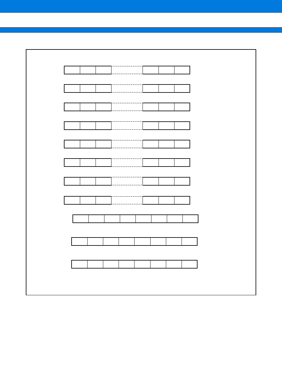
MB91360G Series
119
(Continued)
Area Mask Register (AMR0 to AMR7)
Area Mode Registers (AMD0 to AMD7)
CHE (CacHe Enable register)
CSE (Chip Select Enable register)
AMR0
Initial value
Access
INIT
RST
00000642
H
FFFF
H
FFFF
H
W
AMR1
Initial value
Access
INIT
RST
00000646
H
0000
H
XXXX
H
W
AMR2
Initial value
Access
INIT
RST
0000064A
H
0000
H
XXXX
H
W
AMR3
Initial value
Access
INIT
RST
0000064E
H
0000
H
XXXX
H
W
AMR4
Initial value
Access
INIT
RST
0000652
H
0000
H
XXXX
H
W
AMR5
Initial value
Access
INIT
RST
00000656
H
0000
H
XXXX
H
W
AMR6
Initial value
Access
INIT
RST
0000065A
H
0000
H
XXXX
H
W
AMR7
Initial value
Access
INIT
RST
0000065E
H
0000
H
XXXX
H
W
00000660
H
00000111
B
R
/
W
00000670
H
11111111
B
R
/
W
00000668
H
00000001
B
R
/
W
15
14
13
12
2
1
0
A30
A31
A29
PO4
PO3
A18
A17
A16
. . .
. . .
. . .
15
14
13
12
2
1
0
A30
A31
A29
PO4
PO3
A18
A17
A16
. . .
. . .
. . .
15
14
13
12
2
1
0
A30
A31
A29
PO4
PO3
A18
A17
A16
. . .
. . .
. . .
15
14
13
12
2
1
0
A30
A31
A29
PO4
PO3
A18
A17
A16
. . .
. . .
. . .
15
14
13
12
2
1
0
A30
A31
A29
PO4
PO3
A18
A17
A16
. . .
. . .
. . .
15
14
13
12
2
1
0
A30
A31
A29
PO4
PO3
A18
A17
A16
. . .
. . .
. . .
15
14
13
12
2
1
0
A30
A31
A29
PO4
PO3
A18
A17
A16
. . .
. . .
. . .
15
14
13
12
2
1
0
A30
A31
A29
PO4
PO3
A18
A17
A16
. . .
. . .
. . .
RDYE
BW1
BW0
WTC2
WTC1
WTC0
CHE6
CHE7
CHE5
CHE4
CHE3
CHE2
CHE1
CHE0
CSE6
CSE7
CSE5
CSE4
CSE3
CSE2
CSE1
CSE0
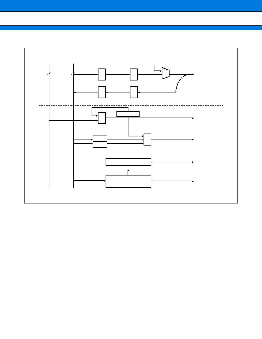
MB91360G Series
120
(2) Block Diagram
MUX
ADDRESS BUS DATA BUS
CS0X to CS7X
RDX
WR0X, WR1X
WR2X, WR3X
BRQ
BGRNTX
RDY
CLK
32
32
write bus
read buffer
switch
A-OUT
switch
+
1 or
+
2
address buffer
ASR
ASZ
comparator
All block control
DATA BLOCK
EXTERNAL
DATA BUS
EXTERNAL
ADDRESS BUS
ADDRESS BLOCK
resisters
&
control
External pin control section

MB91360G Series
121
17. CAN CONTROLLER
This section provides an overview of the CAN Interface, describes the register structure and functions, and
describes the operation of the CAN Interface.
The CAN controller is a module built into a MB91360G series. The CAN (Controller Area Network) is the standard
protocol for serial communication between automobile controllers and is widely used in industrial applications.
The CAN controller has the following features :
∑ Conforms to CAN Specification Version 2.0 Part A and B
- Supports transmission/reception in standard frame and extended frame formats
∑ Supports transmitting of data frames by receiving remote frames
∑ 16 transmitting/receiving message buffers
- 29-bit ID and 8-byte data
- Multi-level message buffer configuration
∑ Supports full-bit comparison, full-bit mask and partial bit mask filtering.
- Two acceptance mask registers in either standard frame format or extended frame formats
∑ Bit rate programmable from 10 Kbits/s to 1 Mbits/s (when input clock is at 16 MHz)
The following sections only describe CAN 0. For the addresses of the registers of the other CAN channels see
the IO-Map.
The address shown assume that the CS7 area is defined as described in the chapter about the internal Boot ROM.
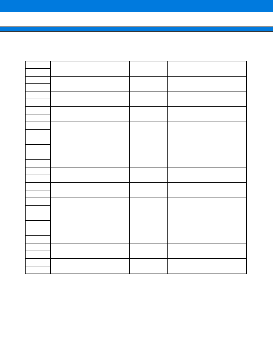
MB91360G Series
122
(1) List of Control Registers
List of Control Registers (1)
Address
Register
Abbreviation
Access
Initial Value
CAN0
100000
H
Message buffer valid register
BVALR0
R/W
00000000 00000000
100001
H
100002
H
Transmit request register
TREQR0
R/W
00000000 00000000
100003
H
100004
H
Transmit cancel register
TCANR0
W
00000000 00000000
100005
H
100006
H
Transmit complete register
TCR0
R/W
00000000 00000000
100007
H
100008
H
Receive complete register
RCR0
R/W
00000000 00000000
100009
H
10000A
H
Remote request receiving register
RRTRR0
R/W
00000000 00000000
10000B
H
10000C
H
Receive overrun register
ROVRR0
R/W
00000000 00000000
10000D
H
10000E
H
Receive interrupt enable register
RIER0
R/W
00000000 00000000
10000F
H
100010
H
Control status register
CSR0
R/W, R
00
-
-
-
000 0
-
-
-
-
0
-
1
100011
H
100012
H
Last event indicator register
LEIR0
R/W
-
-
-
-
-
-
-
- 000
-
0000
100013
H
100014
H
Receive/transmit error counter
RTEC0
R
00000000 00000000
100015
H
100016
H
Bit timing register
BTR0
R/W
-1111111 11111111
100017
H
100018
H
IDE register
IDER0
R/W
XXXXXXXX XXXXXXXX
100019
H
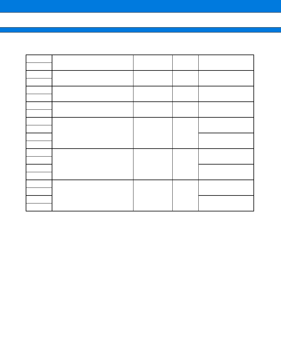
MB91360G Series
123
List of Control Registers (2)
Address
Register
Abbreviation
Access
Initial Value
CAN0
10001A
H
Transmit RTR register
TRTRR0
R/W
00000000 00000000
10001B
H
10001C
H
Remote frame receive waiting register
RFWTR0
R/W
XXXXXXXX XXXXXXXX
10001D
H
10001E
H
Transmit interrupt enable register
TIER0
R/W
00000000 00000000
10001F
H
100020
H
Acceptance mask select register
AMSR0
R/W
XXXXXXXX XXXXXXXX
100021
H
100022
H
XXXXXXXX XXXXXXXX
100023
H
100024
H
Acceptance mask register 0
AMR00
R/W
XXXXXXXX XXXXXXXX
100025
H
100026
H
XXXXX
-
-
- XXXXXXXX
100027
H
100028
H
Acceptance mask register 1
AMR10
R/W
XXXXXXXX XXXXXXXX
100029
H
10002A
H
XXXXX
-
-
- XXXXXXXX
10002B
H
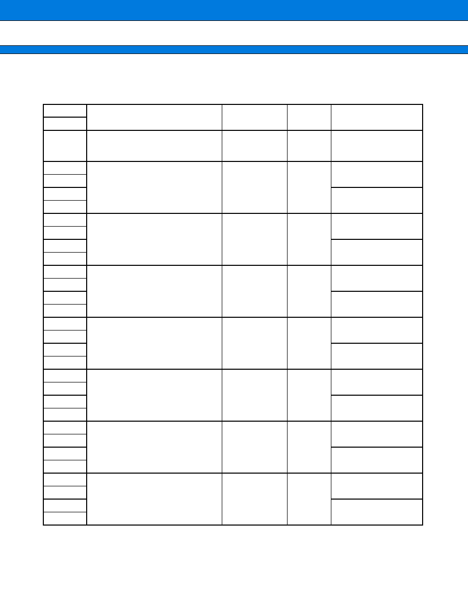
MB91360G Series
124
(2) Message Buffers
List of Message Buffers (ID Registers) (1)
Address
Register
Abbreviation
Access
Initial Value
CAN0
10002C
H
to
10004B
H
General-purpose RAM
R/W
XXXXXXXX
to
XXXXXXXX
10004C
H
ID register 0
IDR00
R/W
XXXXXXXX XXXXXXXX
10004D
H
10004E
H
XXXXX
-
-
- XXXXXXXX
10004F
H
100050
H
ID register 1
IDR10
R/W
XXXXXXXX XXXXXXXX
100051
H
100052
H
XXXXX
-
-
- XXXXXXXX
100053
H
100054
H
ID register 2
IDR20
R/W
XXXXXXXX XXXXXXXX
100055
H
100056
H
XXXXX
-
-
- XXXXXXXX
100057
H
100058
H
ID register 3
IDR30
R/W
XXXXXXXX XXXXXXXX
100059
H
10005A
H
XXXXX
-
-
- XXXXXXXX
10005B
H
10005C
H
ID register 4
IDR40
R/W
XXXXXXXX XXXXXXXX
10005D
H
10005E
H
XXXXX
-
-
- XXXXXXXX
10005F
H
100060
H
ID register 5
IDR50
R/W
XXXXXXXX XXXXXXXX
100061
H
100062
H
XXXXX
-
-
- XXXXXXXX
100063
H
100064
H
ID register 6
IDR60
R/W
XXXXXXXX XXXXXXXX
100065
H
100066
H
XXXXX
-
-
- XXXXXXXX
100067
H
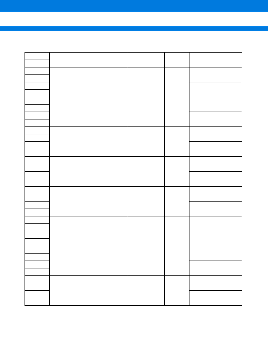
MB91360G Series
125
List of Message Buffers (ID Registers) (2)
Address
Register
Abbreviation
Access
Initial Value
CAN0
100068
H
ID register 7
IDR70
R/W
XXXXXXXX XXXXXXXX
100069
H
10006A
H
XXXXX
-
-
- XXXXXXXX
10006B
H
10006C
H
ID register 8
IDR80
R/W
XXXXXXXX XXXXXXXX
10006D
H
10006E
H
XXXXX
-
-
- XXXXXXXX
10006F
H
100070
H
ID register 9
IDR90
R/W
XXXXXXXX XXXXXXXX
100071
H
100072
H
XXXXX
-
-
- XXXXXXXX
100073
H
100074
H
ID register 10
IDR10
R/W
XXXXXXXX XXXXXXXX
100075
H
100076
H
XXXXX
-
-
- XXXXXXXX
100077
H
100078
H
ID register 11
IDR11
R/W
XXXXXXXX XXXXXXXX
100079
H
10007A
H
XXXXX
-
-
- XXXXXXXX
10007B
H
10007C
H
ID register 12
IDR12
R/W
XXXXXXXX XXXXXXXX
10007D
H
10007E
H
XXXXX
-
-
- XXXXXXXX
10007F
H
100080
H
ID register 13
IDR13
R/W
XXXXXXXX XXXXXXXX
100081
H
100082
H
XXXXX
-
-
- XXXXXXXX
100083
H
100084
H
ID register 14
IDR14
R/W
XXXXXXXX XXXXXXXX
100085
H
100086
H
XXXXX
-
-
- XXXXXXXX
100087
H
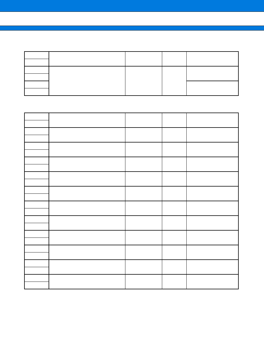
MB91360G Series
126
List of Message Buffers (ID Registers) (3)
List of Message Buffers (DLC Registers and Data Registers) (1)
Address
Register
Abbreviation
Access
Initial Value
CAN0
100088
H
ID register 15
IDR15
R/W
XXXXXXXX XXXXXXXX
100089
H
10008A
H
XXXXX
-
-
- XXXXXXXX
10008B
H
Address
Register
Abbreviation
Access
Initial Value
CAN0
10008C
H
DLC register 0
DLCR00
R/W
-
-
-
-
XXXX
10008D
H
10008E
H
DLC register 1
DLCR10
R/W
-
-
-
-
XXXX
10008F
H
100090
H
DLC register 2
DLCR20
R/W
-
-
-
-
XXXX
100091
H
100092
H
DLC register 3
DLCR30
R/W
-
-
-
-
XXXX
100093
H
100094
H
DLC register 4
DLCR40
R/W
-
-
-
-
XXXX
100095
H
100096
H
DLC register 5
DLCR50
R/W
-
-
-
-
XXXX
100097
H
100098
H
DLC register 6
DLCR60
R/W
-
-
-
-
XXXX
100099
H
10009A
H
DLC register 7
DLCR70
R/W
-
-
-
-
XXXX
10009B
H
10009C
H
DLC register 8
DLCR80
R/W
-
-
-
-
XXXX
10009D
H
10009E
H
DLC register 9
DLCR90
R/W
-
-
-
-
XXXX
10009F
H
1000A0
H
DLC register 10
DLCR100
R/W
-
-
-
-
XXXX
1000A1
H
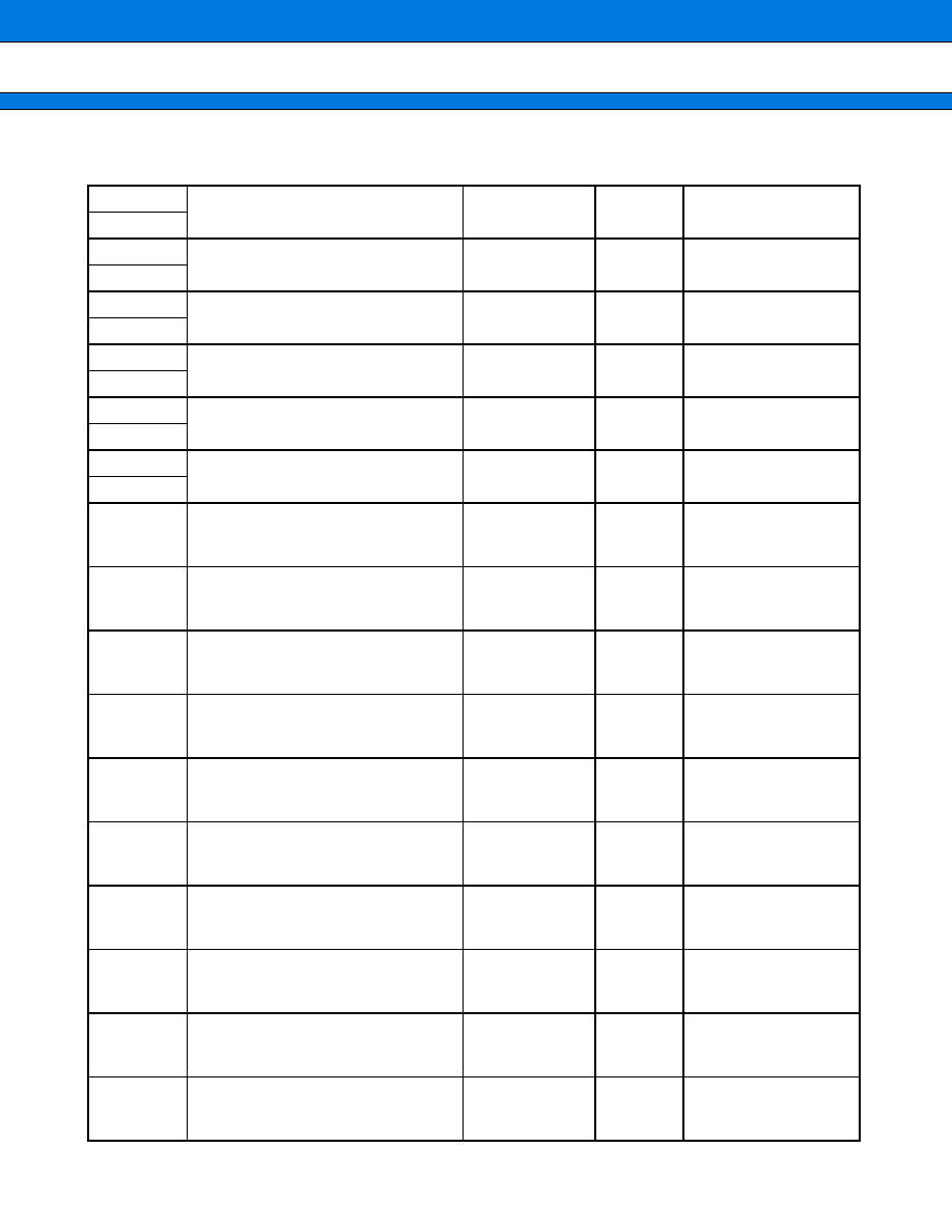
MB91360G Series
127
List of Message Buffers (DLC Registers and Data Registers) (2)
Address
Register
Abbreviation
Access
Initial Value
CAN0
1000A2
H
DLC register 11
DLCR110
R/W
-
-
-
-
XXXX
1000A3
H
1000A4
H
DLC register 12
DLCR120
R/W
-
-
-
-
XXXX
1000A5
H
1000A6
H
DLC register 13
DLCR130
R/W
-
-
-
-
XXXX
1000A7
H
1000A8
H
DLC register 14
DLCR140
R/W
-
-
-
-
XXXX
1000A9
H
1000AA
H
DLC register 15
DLCR150
R/W
-
-
-
-
XXXX
1000AB
H
1000AC
H
to
1000B3
H
Data register 0 (8 bytes)
DTR00
R/W
XXXXXXXX
to
XXXXXXXX
1000B4
H
to
1000BB
H
Data register 1 (8 bytes)
DTR10
R/W
XXXXXXXX
to
XXXXXXXX
1000BC
H
to
1000C3
H
Data register 2 (8 bytes)
DTR20
R/W
XXXXXXXX
to
XXXXXXXX
1000C4
H
to
1000CB
H
Data register 3 (8 bytes)
DTR30
R/W
XXXXXXXX
to
XXXXXXXX
1000CC
H
to
1000D3
H
Data register 4 (8 bytes)
DTR40
R/W
XXXXXXXX
to
XXXXXXXX
1000D4
H
to
1000DB
H
Data register 5 (8 bytes)
DTR50
R/W
XXXXXXXX
to
XXXXXXXX
1000DC
H
to
1000E3
H
Data register 6 (8 bytes)
DTR60
R/W
XXXXXXXX
to
XXXXXXXX
1000E4
H
to
1000EB
H
Data register 7 (8 bytes)
DTR70
R/W
XXXXXXXX
to
XXXXXXXX
1000EC
H
to
1000F3
H
Data register 8 (8 bytes)
DTR80
R/W
XXXXXXXX
to
XXXXXXXX
1000F4
H
to
1000FB
H
Data register 9 (8 bytes)
DTR90
R/W
XXXXXXXX
to
XXXXXXXX
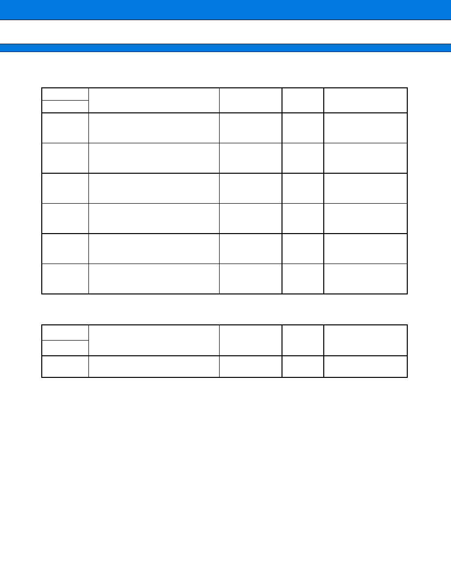
MB91360G Series
128
List of Message Buffers (DLC Registers and Data Registers) (3)
Configuration Register (CREG)
Address
Register
Abbreviation
Access
Initial Value
CAN0
1000FC
H
to
100103
H
Data register 10 (8 bytes)
DTR100
R/W
XXXXXXXX
to
XXXXXXXX
100104
H
to
10010B
H
Data register 11 (8 bytes)
DTR110
R/W
XXXXXXXX
to
XXXXXXXX
10010C
H
to
100113
H
Data register 12 (8 bytes)
DTR120
R/W
XXXXXXXX
to
XXXXXXXX
100114
H
to
10011B
H
Data register 13 (8 bytes)
DTR130
R/W
XXXXXXXX
to
XXXXXXXX
10011C
H
to
100123
H
Data register 14 (8 bytes)
DTR140
R/W
XXXXXXXX
to
XXXXXXXX
100124
H
to
10012B
H
Data register 15 (8 bytes)
DTR150
R/W
XXXXXXXX
to
XXXXXXXX
Address
Register
Abbreviation
Access
Initial Value
CAN0
10012C
H
10012D
H
Configuration register
CREG0
R/W
00000000
00000110
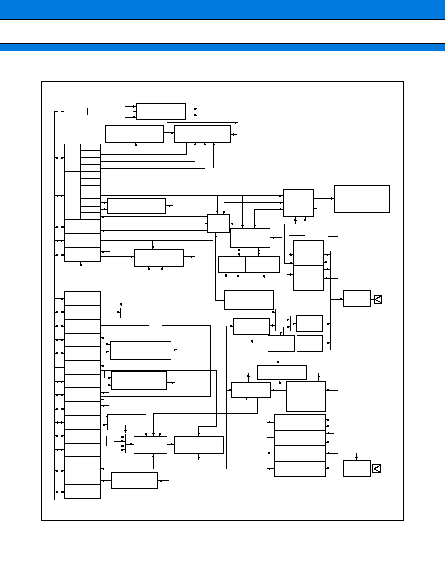
MB91360G Series
129
(3) Block Diagram
BTR
PSC
CREG
CANCLK
CLKT
PR
PH
RSJ
TOE
NS1,0
NT
NIE
HALT
RS
TS
CSR
RTEC
BVALR
TREQR
TCANR
TRTRR
RFWTR
TCR
TIER
RCR
RIER
RRTRR
ROVRR
AMSR
AMR0
AMR1
LEIR
IDR0 to 15,
DLCR0 to
15,
DTR0 to 15,
RAM
0
1
RBF
X
, TBF
X
, RDLC, TDLC, IDSEL
RBF
X
IDSEL
TBF
X
TBF
X
PH1
RX
FRMER
ACKER
BITER
ARBLOST
STFER
RDLC
CRCER
TDLC
TDLC RDLC
IDSEL
ARBLOST
TX
BITER, STFER,
CRCER, FRMER,
ACKER
SYNC, TSEG1, TSEG2
TQ (Operating clock)
Clock
Configuration
Clock for CAN transmit/receive operation
Clock for External Bus Access
External Bus
(User Logic Bus)
Prescaler 1 to 64
frequency division
Bit timing generation
Node status change
interrupt generation
Node status
change interrupt
Bus
state
machine
IDLE, INT, SUSPND,
transmit, receive,
ERR, OVRLD
Error
control
Transmitting/
receiving
sequencer
TBFx,
clear
Transmitting
buffer x decision
Data
counter
Acceptance
filter control
Error
frame
generation
Overload
frame
generation
Output
driver
Transmission
shift register
Stuffing
TBFx, set, clear
CRC
generation
ACK
generation
Transmission complete
interrupt generator
Transmission
complete
interrupt
RBFx, set
CRC generator/
error check
Reception complete
interrupt generation
Reception
completed
interrupt
RBFx, TBFx, set, clear
Receive
shift register
Destuffing/
stuffing
error check
RBFx, set
Arbitration
check
Bit error
check
Acceptance
filter
Receiving buffer x
decision
Acknowledgment
error check
Form error
check
Input
latch
RAM address
generation
MB91360G Series
130
18. D/A CONVERTER
This section provides an overview of the D/A converter, describes the register structure and functions, and
describes the operarton of D/A converter.This block is an R-2R format D/A converter, having ten-bit resolution.
The D/A converter has two channels.Output control can be performed independently for the two channels using
the D/A control register.
(1) Block Diagram
DA
17
DA
16
DA
15
DA
19
DA
18
DA
14
DA
13
DA
12
DA
11
DA
10
DA
07
DA
06
DA
05
DA
09
R-Bus
DA
08
DA
04
DA output ch1
DA output ch0
DA
03
DA
02
DA
01
DA
00
DAE1
Standby control
2R
2R
2R
2R
R
R
R
DVR
DA19
DA18
DA17
DA11
DA10
DAE0
Standby control
2R
2R
2R
2R
R
R
R
DVR
DA09
DA08
DA07
DA01
DA00
2R
2R
MB91360G Series
131
(2) Registers
D/A control register (DACR)
D/A converter data register (ch 0) (DADR0)
D/A converter data register (ch 1) (DADR1)
D/A clock control (DDBL)
bit
Address : 0000A5
H
bit
Address : 0000A6
H
bit
Address : 0000A7
H
bit
Address : 0000A8
H
bit
Address : 0000A9
H
bit
Address : 0000AB
H
7
6
5
4
3
2
1
0
MODE
DAE1
DAE0
15
14
13
12
11
10
9
8
DA09
DA08
7
6
5
4
3
2
1
0
DA06
DA07
DA05
DA04
DA03
DA02
DA01
DA00
15
14
13
12
11
10
9
8
DA19
DA18
7
6
5
4
3
2
1
0
DA16
DA17
DA15
DA14
DA13
DA12
DA11
DA10
7
6
5
4
3
2
1
0
DBL

MB91360G Series
132
19. 100 kHz I
2
C INTERFACE
This section describes the functions and operation of the MB91360G series basic I
2
C interface. This interface
allows operation up to 100 kHz and 8-bit-addressing.
The I
2
C interface is a serial I/O port supporting the Inter IC bus, operating as a master/slave device on the I
2
C bus.
(1) I
2
C Interface Features
The MB91360G series microcontroller includes a built-in one-channel I
2
C interface. The I
2
C interface has the
following features.
∑ Master/slave sending and receiving functions
∑ Arbitration function
∑ Clock synchronization function
∑ Slave address/general call address detection function
∑ Transfer direction detection function
∑ Repeated start condition generation and detection function
∑ Bus error detection function
MB91360G Series
133
(2) I
2
C Interface Registers
a : Bus Status Register (IBSR)
b : Bus Control Register (IBCR)
c : Clock control register (ICCR)
d : Address Register (IADR)
e : Data Register (IDAR)
f : Clock Disable Register (IDBL)
Bit no.
Address : 000095
H
Read/write
Default value
Bit no.
Address : 000094
H
Read/write
Default value
Bit no.
Address : 000097
H
Read/write
Default value
Bit no.
Address : 000096
H
Read/write
Default value
Bit no.
Address : 000099
H
Read/write
Default value
Bit no.
Address : 00009B
H
Read/write
Default value
( R )
( 0 )
( R )
( 0 )
( R )
( 0 )
( R )
( 0 )
( R )
( 0 )
( R )
( 0 )
( R )
( 0 )
7
6
5
4
3
2
1
0
RSC
( R )
( 0 )
BB
AL
LRB
TRX
AAS
GCA
FBT
(R/W)
( 0 )
(R/W)
( 0 )
(R/W)
( 0 )
(R/W)
( 0 )
(R/W)
( 0 )
(R/W)
( 0 )
(R/W)
( 0 )
15
14
13
12
11
10
9
8
BEIE
(R/W)
( 0 )
BER
SCC
MSS
ACK
GCAA
INTE
INT
(
)
(
)
(R/W)
( 0 )
(R/W)
( X )
(R/W)
( X )
(R/W)
( X )
(R/W)
( X )
(R/W)
( X )
7
6
5
4
3
2
1
0
(
)
(
)
EN
CS4
CS3
CS2
CS1
CS0
(R/W)
( X )
(R/W)
( X )
(R/W)
( X )
(R/W)
( X )
(R/W)
( X )
(R/W)
( X )
(R/W)
( X )
15
14
13
12
11
10
9
8
A6
(
)
(
)
A5
A4
A3
A2
A1
A0
(R/W)
( X )
(R/W)
( X )
(R/W)
( X )
(R/W)
( X )
(R/W)
( X )
(R/W)
( X )
(R/W)
( X )
7
6
5
4
3
2
1
0
D6
(R/W)
( X )
D7
D5
D4
D3
D2
D1
D0
(
)
(
)
(
)
(
)
(
)
(
)
(
)
(
)
(
)
(
)
(
)
(
)
(R/W)
( 0 )
7
6
5
4
3
2
1
0
(
)
(
)
DBL
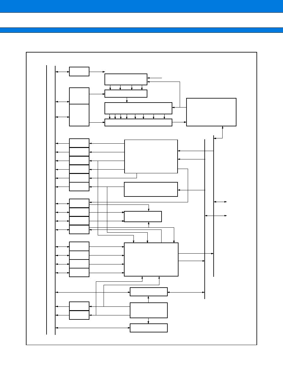
MB91360G Series
134
(3) I
2
C Interface Block Diagram
ICCR
EN
ICCR
IBSR
BB
RSC
LRB
TRX
FBT
AL
IBCR
BER
BEIE
INTE
INT
IBCR
R-bus
SCC
MSS
ACK
GCAA
IBSR
IDAR
IADR
AAS
GCA
CS4
CS3
CS2
CS1
CS0
2 4
8 16
128
256
32
64
5
6
7
8
Sync
Shift clock generator
Start-stop condition
deector
Arbitration lost detectior
Interrupt request
End
Start-stop condition
detector
Slave address
comparator
Clock divider 1
Clock selector 1
Clock divider 2
Clock selector 2
First Byte
Error
I
2
C enable
Clock signal for division
Shift clock edge
conversion timing
Bus busy
Repeat start
Send/receive
Start
Master
Slave
Global call
ACK enable
GC-ACK enable
Last Bit
SCL
SDA

MB91360G Series
135
20. 400 kHz I
2
C INTERFACE
This section describes the functions and operation of the fast I
2
C interface.
The I
2
C interface is a serial I/O port supporting the Inter IC bus, operating as a master/slave device on the I
2
C bus.
(1) Features
∑ Master/slave transmitting and receiving functions
∑ Arbitration function
∑ Clock synchronization function
∑ General call addressing support
∑ Transfer direction detection function
∑ Repeated start condition generation and detection function
∑ Bus error detection function
∑ 7 bit addressing as master and slave
∑ 10 bit addressing as master and slave
∑ Possibility to give the interface a seven and a ten bit slave address
∑ Acknowledging upon slave address reception can be disabled (Master-only operation)
∑ Address masking to give interface several slave addresses (in 7 and 10 bit mode)
∑ Up to 400 KBit transfer rate
∑ Possibility to use built-in noise filters for SDA and SCL
∑ Can receive data at 400 KBit if R-Bus-Clock is higher than 6 MHz regardless of prescaler setting
∑ Can generate MCU interrupts on transmission and bus error events
∑ Supports being slowed down by a slave on bit and byte level
The I
2
C interface does not support SCL clock stretching on bit level since it can receive the full 400 KBit datarate
if the R-Bus-Clock (CLKP) is higher than 6 MHz regardless of the prescaler setting. However, clock stretching
on byte level is performed since SCL is pulled low during an interrupt (INT
=
"1" in IBCR register) .
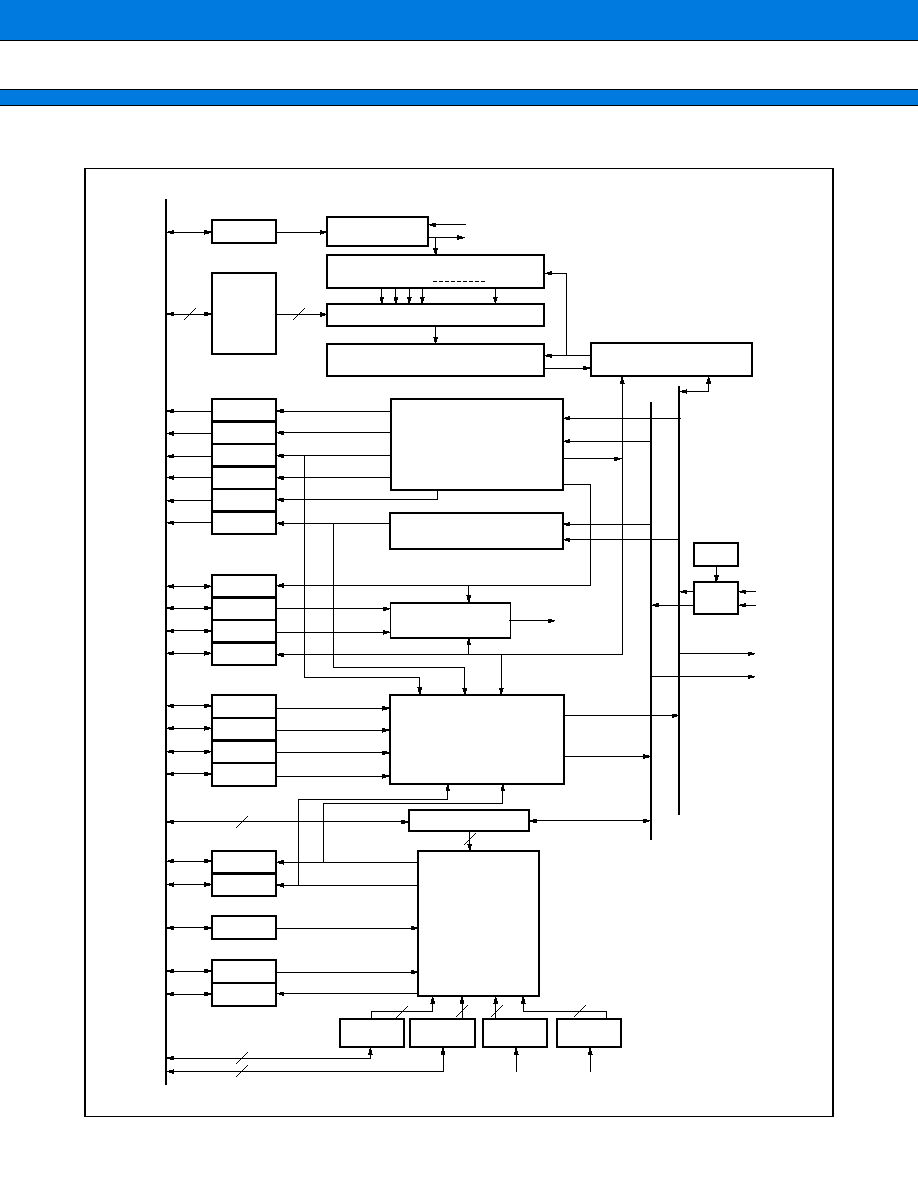
MB91360G Series
136
(2) Block Diagram
IDBL
DBL
Clock disable
Clock Divider 1
Clock Selector
Clock Divider 2 (by 12)
SCL Duty Cycle Generator
ICCR
5
5
IBSR
BB
RSC
LRB
TRX
ADT
AL
IBCR
BER
BEIE
INTE
INT
IBCR
R-bus
SCC
MSS
ACK
GCAA
IBSR
IDAR
AAS
GCA
ISMK
ITMK
ENTB
RAL
ITMK
ITBA
ISBA
ISMK
ENSB
CS4
CS3
CS2
CS1
CS0
2 3 4 5
32
Sync
Interrupt Request
Start-Stop Condition
Generator
ACK Generator
Slave Address
Comparator
Bus Observer
Arbitration Loss Detector
Shift Clock Generator
Address Data
Bus Error
MCU
IRQ
SCL
SDA
SCL
enable
SDA
Bus busy
R-Bus Clock (CLKP)
FB59 Module Clock Supply
Repeat start
Send/receive
Start
Master
Slave
General call
ACK enable
GC-ACK enable
enable 7 bit mode
enable 10 bit mode
received ad. length
Last Bit
NSF
Noise
Filter
ICCR
8
10
10
7
10
7
10
8
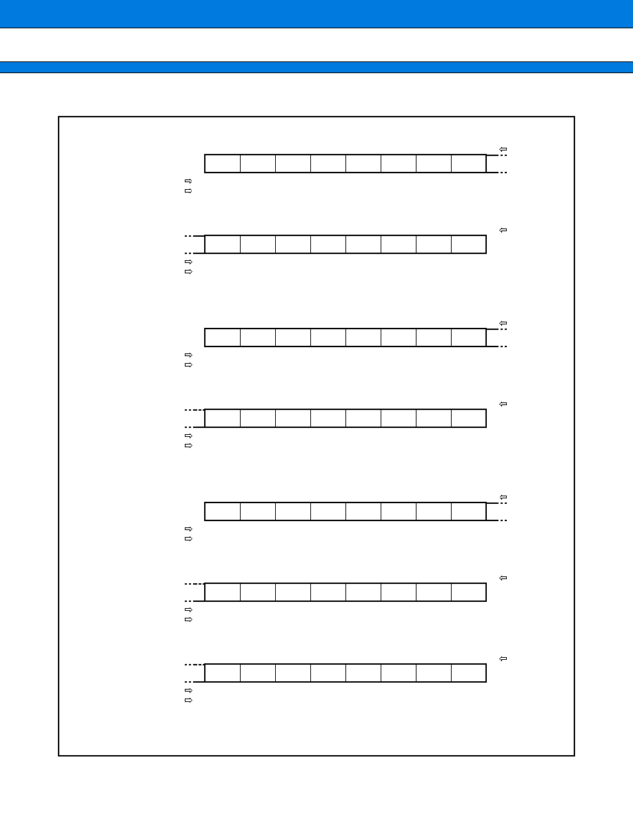
MB91360G Series
137
(3) I
2
C Interface Registers
(Continued)
a : Bus Control Register (IBCR2)
b : Bus Status Register (IBSR2)
c : Ten Bit slave Address register (ITBAH, ITBAL)
Ten Bit Address high byte
Ten Bit Address low byte
d : Ten bit slave address Mask register (ITMKH, ITMKL)
Ten Bit Address Mask high byte
Ten Bit Address Mask low byte
e : Seven Bit slave Address register (ISBA)
Bit no.
Address : 000184
H
Read/write
Default value
Bit no.
Address : 000185
H
Read/write
Default value
Bit no.
Address : 000186
H
Read/write
Default value
Bit no.
Address : 000187
H
Read/write
Default value
Bit no.
Address : 000188
H
Read/write
Default value
Bit no.
Address : 000189
H
Read/write
Default value
Bit no.
Address : 00018B
H
Read/write
Default value
(R/W)
( 0 )
( W )
( 0 )
(R/W)
( 0 )
(R/W)
( 0 )
(R/W)
( 0 )
(R/W)
( 0 )
(R/W)
( 0 )
15
14
13
12
11
10
9
8
BEIE
(R/W)
( 0 )
BER
SCC
MSS
ACK
GCAA
INTE
INT
( R )
( 0 )
( R )
( 0 )
( R )
( 0 )
( R )
( 0 )
( R )
( 0 )
( R )
( 0 )
( R )
( 0 )
7
6
5
4
3
2
1
0
RSC
( R )
( 0 )
BB
AL
LRB
TRX
AAS
GCA
FBT
(
)
( 0 )
(
)
( 0 )
(
)
( 0 )
(
)
( 0 )
(
)
( 0 )
(R/W)
( 0 )
(R/W)
( 0 )
15
14
13
12
11
10
9
8
(
)
( 0 )
TA9
TA8
(R/W)
( 0 )
(R/W)
( 0 )
(R/W)
( 0 )
(R/W)
( 0 )
(R/W)
( 0 )
(R/W)
( 0 )
(R/W)
( 0 )
7
6
5
4
3
2
1
0
TA6
(R/W)
( 0 )
TA7
TA5
TA4
TA3
TA2
TA1
TA0
( R )
( 0 )
(
)
( 1 )
(
)
( 1 )
(
)
( 1 )
(
)
( 1 )
(R/W)
( 1 )
(R/W)
( 1 )
15
14
13
12
11
10
9
8
RAL
(R/W)
( 0 )
ENTB
TM9
TM8
(R/W)
( 1 )
(R/W)
( 1 )
(R/W)
( 1 )
(R/W)
( 1 )
(R/W)
( 1 )
(R/W)
( 1 )
(R/W)
( 1 )
7
6
5
4
3
2
1
0
TM6
(R/W)
( 1 )
TM7
TM5
TM4
TM3
TM2
TM1
TM0
(R/W)
( 0 )
(R/W)
( 0 )
(R/W)
( 0 )
(R/W)
( 0 )
(R/W)
( 0 )
(R/W)
( 0 )
(R/W)
( 0 )
7
6
5
4
3
2
1
0
SA6
(
)
( 0 )
SA5
SA4
SA3
SA2
SA1
SA0
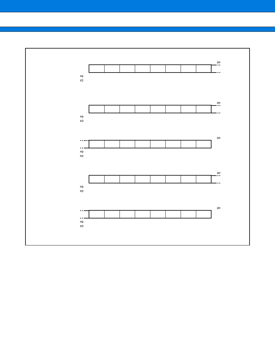
MB91360G Series
138
(Continued)
f : Seven bit slave address Mask register (ISMK)
g : Data Register (IDARH, IDAR2)
Data register high byte
Data register
h : Clock control register (ICCR2)
i : Clock Disable Register (IDBL2)
Bit no.
Address : 00018A
H
Read/write
Default value
Bit no.
Address : 00018C
H
Read/write
Default value
Bit no.
Address : 00018D
H
Read/write
Default value
Bit no.
Address : 00018E
H
Read/write
Default value
Bit no.
Address : 00018F
H
Read/write
Default value
(R/W)
( 1 )
(R/W)
( 1 )
(R/W)
( 1 )
(R/W)
( 1 )
(R/W)
( 1 )
(R/W)
( 1 )
(R/W)
( 1 )
15
14
13
12
11
10
9
8
SM6
(R/W)
( 0 )
ENSB
SM5
SM4
SM3
SM2
SM1
SM0
(
)
( 0 )
(
)
( 0 )
(
)
( 0 )
(
)
( 0 )
(
)
( 0 )
(
)
( 0 )
(
)
( 0 )
15
14
13
12
11
10
9
8
(
)
( 0 )
(R/W)
( 0 )
(R/W)
( 0 )
(R/W)
( 0 )
(R/W)
( 0 )
(R/W)
( 0 )
(R/W)
( 0 )
(R/W)
( 0 )
7
6
5
4
3
2
1
0
D6
(R/W)
( 0 )
D7
D5
D4
D3
D2
D1
D0
(R/W)
( 0 )
(R/W)
( 0 )
(R/W)
( 1 )
(R/W)
( 1 )
(R/W)
( 1 )
(R/W)
( 1 )
(R/W)
( 1 )
15
14
13
12
11
10
9
8
NSF
(
)
( 0 )
EN
CS4
CS3
CS2
CS1
CS0
(
)
( 0 )
(
)
( 0 )
(
)
( 0 )
(
)
( 0 )
(
)
( 0 )
(
)
( 0 )
(R/W)
( 0 )
7
6
5
4
3
2
1
0
(
)
( 0 )
DBL

MB91360G Series
139
21. 16-BIT I/O TIMER
The MB91360G Series contains two 16-bit free-running timer modules, two output compare modules, and two
input capture modules and supports four input channels and four output channels. The following sections only
describes the 16-bit free-running timer, Output Compare 0/1 and Input Capture 0/1.
The remaining modules have the identical functions and the register addresses should be found in the I/O map.
(1) Function Overview
a : 16-bit free-running timer
The 16-bit free-run timer consists of a 16-bit up counter, control register, and prescaler. The values output from
this timer counter are used as the base timer for input capture and output compare.
∑ Four counter clocks are available.
Internal clock :
/4,
/16,
/32,
/64
∑ An interrupt can be generated upon a counter overflow or a match with compare register 0.
∑ The counter value can be initialized to "0000H" upon a reset, software clear, or match with compare register 0.
b : Output compare (2 channels per one module)
The output compare module consists of two 16-bit compare registers, compare output latch, and control register.
When the 16-bit free-running timer value matches the compare register value, the output level is reversed and
an interrupt is issued.
∑ The two compare registers can be used independently.
Output pins and interrupt flags corresponding to compare registers
∑ Output pins can be controlled based on pairs of the two compare registers.
Output pins can be reversed by using the two compare registers.
∑ Initial values for output pins can be set.
∑ Interrupts can be generated upon a compare match.
c : Input capture (2 channels per one module)
The input capture module consists of two 16-bit capture registers and control registers corresponding to two
independent external input pins. The 16-bit free-running timer value can be stored in the capture register and
an interrupt is issued simultaneously upon detection of an edge of a signal input from an external input pin.
∑ The detection edge of an external input signal can be specified.
Rising, falling, or both edges
∑ Two input channels can operate independently.
∑ An interrupt can be issued upon a valid edge of an external input signal.
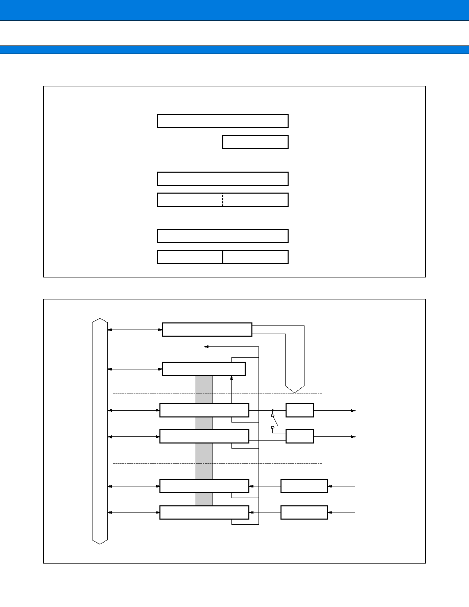
MB91360G Series
140
(2) Registers
(3) Block Diagram
a : 16-bit free-running timer
b : 16-bit output compare
c : 16-bit input capture
TCDT
TCCS
Timer data register
Timer status register
15
0
0000CB
H
0000C8
H
OCCP0/1
OCS0
OCS1
Compare register
Control status register
15
0
0000B8
H
0000BC
H
0000BE
H
IPC0/1
ICS0/1
IOTDBL0
Capture register
Disable/Control status register
15
0
0000AC
H
0000B0
H
0000B2
H
TQ
Control logic
T
o
each b
loc
k
16-bit timer
Compare register 0
Bus
TQ
Edge selection
Edge selection
OUT0
Clear
OUT1
IN0
Interrupt
16-bit free-run timer
Output compare 0
Compare register 1
Output compare 1
Capture register 0
Input caputure 0
Capture register 1
Input caputure 1
IN1
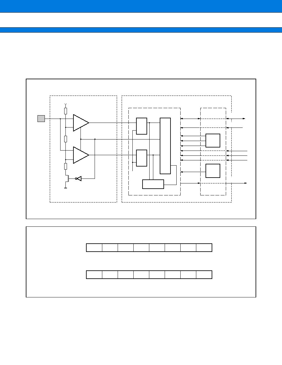
MB91360G Series
141
22. ALARM COMPARATOR
This section provides an overview of the Alarm Comparator (Also called Under/Overvoltage Detection) , de-
scribes the register structure and functions, and describes the operation of the Alarm Comparator.
(1) Block Diagram
(2) Registers
Alarm comparator - analog part
UMQA02
Alarm comparator - digital part
ALARM
OUT1
PD
OUT2
F-MODULE
B-MODULE
FR51
B0DX
ACSR
STOP
STOP
RST
CLKP
CLKP
CLKP
RST
RB [15:0]
RB [15:0]
WRCR
PMWR
RDCR
RSLEEP
CDBLE
IRQ_AC
Interrupt
logic
CK
CK
AV
DD
D Q
D Q
IRQ_AC
CDBLE
REG
RSLEEP
DEC
Alarm Comparator Clock Disable Register (ACCDBL)
Alarm Comparator Status Disable Register (ACSR)
Address
Bits
Initial value
00000180
H
- - - - - - - 0
B
Access
Address
Bits
Initial value
00000181
H
-11xxx00
B
Access
R/W
7
6
5
4
3
2
1
0
CDBLE
R/W
R/W
R
R
R/W
R/W
R/W
7
6
5
4
3
2
1
0
OV_EN
UV-EN
OUT2
OUT1
IRQ
IEN
PD
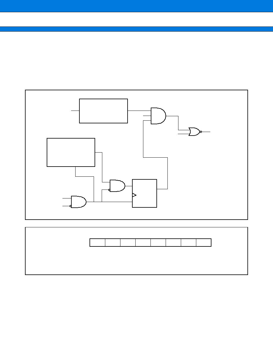
MB91360G Series
142
23. POWER DOWN RESET
This section provides an overview of the Power Down Reset, and describes the register structure.
The power down reset module performs a system reset when V
CC
goes below a threshold voltage. The reset
signal is be disabled and enabled by setting the power down reset control register PDRCR. For low power
applications the digital and the analog part of the power down reset control circuit can be disabled.
(
1
)
Block Diagram
(2) Register
PDCOMP
IN
OUT
input stage
EN
RST
PDRSTX
S
Q
R
9-bit LFSR
counter
READY
CLR
WR
RB [1]
(RD bit)
PDRCR
access
initial value (INIT)
initial value (RST)
X
X
X
X
R/W
0
X
R/W
0
X
R/W
0
X
7
6
5
4
3
2
1
0
X
CDSBLE
PD
EN
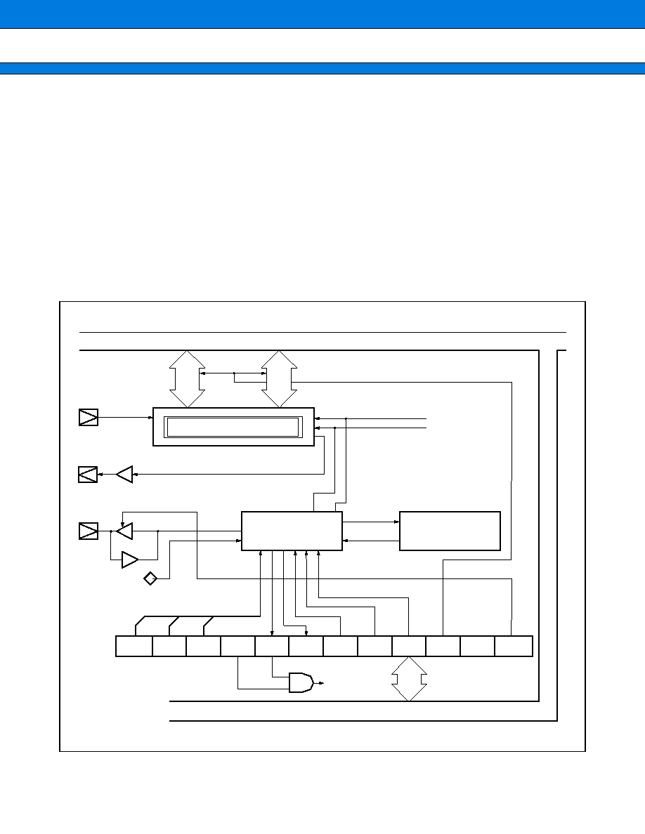
MB91360G Series
143
24. SERIAL I/O INTERFACE (SIO)
This section provides an overview of the Serial I/O Interface (SIO) , and describes the register structure.
(1) Block Diagram
This block is a serial I/O interface that allows data transfer using clock synchronization. The interface consists
of a single eight-bit channel. Data can be transferred from the LSB or MSB.
MB91360G series contains two Serial I/O units SIO0 and SIO1. This section only describes SIO0. Please see
the IO-Map for the register addresses of SIO1.
The serial I/O interface operates in two modes :
∑ Internal shift clock mode : Data is transferred in synchronization with the internal clock.
∑ External shift clock mode : Data is transferred in synchronization with the clock supplied via the external pin
(SCK) . By manipulating the general-purpose port sharing the external pin (SCK) ,
data can also be transferred by a CPU instruc tion in this mode.
Interrupt
request
SIN3
(MSB first) D7 to D0
D7 to D0 (LSB first)
Read
Write
Transfer direction selection
SOT3
SCK3
Internal clock
1
0
2
SMD2
SMD1
SMD0
SIR
SIE
BUSY
STOP
STRT
MODE
BDS
SCOE
Internal data bus
SDR (Serial data register)
Control circuit
Shift clock counter
Internal data bus
MB91360G Series
144
(
2
)
Registers
Serial mode control status register (SMCS)
SIO edge selection/clock disable register (SES)
Serial data register (SDR)
Address : 000084
H
Address : 000085
H
Address : 000086
H
Address : 000087
H
15
14
13
12
11
10
9
8
SMD1
SMD2
SMD0
SIE
SIR
BUSY
STOP
STRT
7
6
5
4
3
2
1
0
MODE
BDS
SCOE
15
14
13
12
11
10
9
8
DBL
NEG
7
6
5
4
3
2
1
0
D6
D7
D5
D4
D3
D2
D1
D0
MB91360G Series
145
25. SOUND GENERATOR
This section provides an overview of the Sound Generator, and describes the register structure.
The Sound Generator consists of the Sound Control register, Frequency Data register, Amplitude Data register,
Decrement Grade register, Tone Count register, Sound Disable register, PWM pulse generator, Frequency
counter, Decrement counter and Tone Pulse counter.
(1) Registers
Sound Control register (SGCR)
Frequency Data register (SGFR)
Amplitude Data register (SGAR)
Decrement Grade register (SGDR)
Tone Count register (SGTR)
Sound Disable register (SGDBL)
Bit no.
Address : 0000EF
H
Read/write
Default value
Bit no.
Address : 0000EE
H
Read/write
Default value
Bit no.
Address : 0000F1
H
Read/write
Default value
Bit no.
Address : 0000F0
H
Read/write
Default value
Bit no.
Address : 0000F3
H
Read/write
Default value
Bit no.
Address : 0000F2
H
Read/write
Default value
Bit no.
Address : 0000ED
H
Read/write
Default value
(R/W)
( 0 )
(R/W)
( 0 )
(
)
(
)
(
)
(
)
(R/W)
( 0 )
(R/W)
( 0 )
(R/W)
( 0 )
7
6
5
4
3
2
1
0
S0
(R/W)
( 0 )
S1
TONE
INTE
INT
ST
(
)
(
)
(
)
(
)
(
)
(
)
(
)
(
)
(
)
(
)
( R )
( 0 )
(R/W)
( 0 )
15
14
13
12
11
10
9
8
(R/W)
( 0 )
TST
BUSY
DEC
(R/W)
( X )
(R/W)
( X )
(R/W)
( X )
(R/W)
( X )
(R/W)
( X )
(R/W)
( X )
(R/W)
( X )
7
6
5
4
3
2
1
0
D6
(R/W)
( X )
D7
D5
D4
D3
D2
D1
D0
(R/W)
( 0 )
(R/W)
( 0 )
(R/W)
( 0 )
(R/W)
( 0 )
(R/W)
( 0 )
(R/W)
( 0 )
(R/W)
( 0 )
15
14
13
12
11
10
9
8
D6
(R/W)
( 0 )
D7
D5
D4
D3
D2
D1
D0
(R/W)
( X )
(R/W)
( X )
(R/W)
( X )
(R/W)
( X )
(R/W)
( X )
(R/W)
( X )
(R/W)
( X )
7
6
5
4
3
2
1
0
D6
(R/W)
( X )
D7
D5
D4
D3
D2
D1
D0
(R/W)
( X )
(R/W)
( X )
(R/W)
( X )
(R/W)
( X )
(R/W)
( X )
(R/W)
( X )
(R/W)
( X )
15
14
13
12
11
10
9
8
(R/W)
( X )
D6
D7
D5
D4
D3
D2
D1
D0
(
)
(
)
(
)
(
)
(
)
(
)
(
)
(
)
(
)
(
)
(
)
(
)
(R/W)
( 0 )
7
6
5
4
3
2
1
0
(
)
(
)
DBL
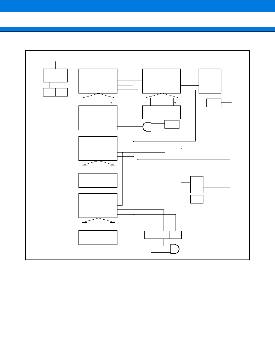
MB91360G Series
146
(2) Block Diagram
S1
S0
TONE
INTE
INT
ST
1/d
DEC
CO
EN
PWM
CI
DEC
CI
CO
EN
CI
CO
EN
CO
EN
D
EN
Q
SGA
SGO
IRQ
Clock input
Prescaler
8-bit PWM
pulse generator
Frequency
counter
Toggle
flip-flop
Reload
Reload
Amplitude data
register
Decrement
Grade register
Decrement
counter
Decrement grade
register
Mix
Tone pulse
counter
Tone count
register
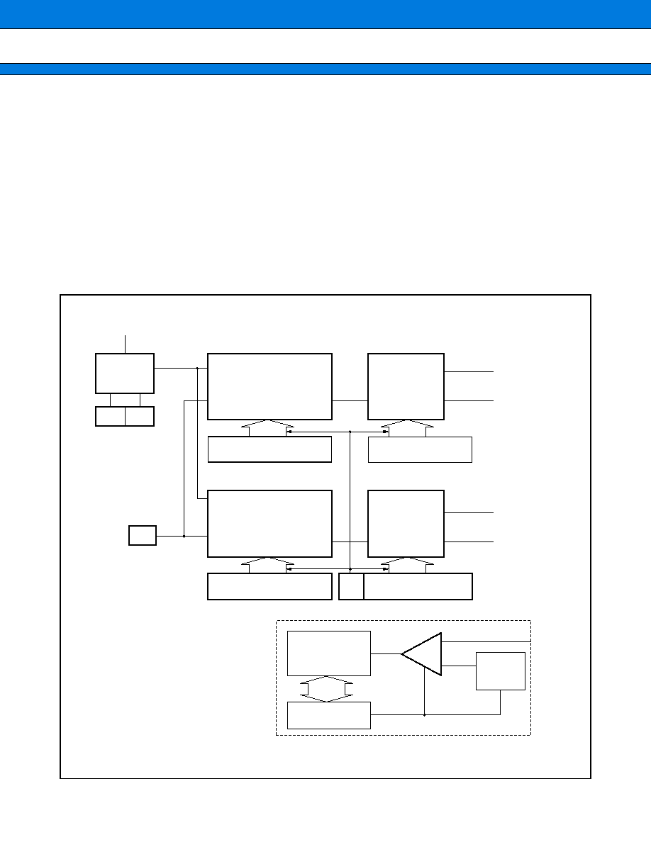
MB91360G Series
147
26. STEPPER MOTOR CONTROLLER
This section provides an overview of the Stepper Motor Control Module, and describe the register structure.
The Stepping Motor Controller consists of two PWM Pulse Generators, four motor drivers, Selector Logic and
the Zero Rotor Position Detector. The four motor drivers have high output drive capabilities and they can be
directly connected to the four ends of two motor coils. The combination of the PWM Pulse Generators and
Selector Logic is designed to control the rotation of the motor. A Synchronization mechanism assures the
synchronous operations of the two PWMs. The Zero Rotor Position Detector helps CPU obtain feed back
information of the rotor movements. The following sections describe the Stepping Motor Controller 0 only. The
other controllers have the same functions. The register addresses are found in the I/O map.
Note : The Rotor Zero Position Detection capability is protected by a patent from siemens VDO automatic AG and
may only be used with VDO's prior approval.
(1) Block Diagram
P1
P0
PWM1P0
PWM2P0
PWM1M0
PWM2M0
PWM2M0
Comparator
Zero Rotor Position Detector
Power down
CE
CK
EN
CK
EN
PWM
PWM
BS
Debounce logic
8-bit counter
1/9 AV
CC
reference
voltage
Machine clock
Prescaler
PWM1 pulse generator
Selector
PWM1 compare register
PWM1 selector register
PWM2 pulse generator
Selector
Load
PWM2 compare register
PWM2 select register
-
+
Zero Detect 0
register
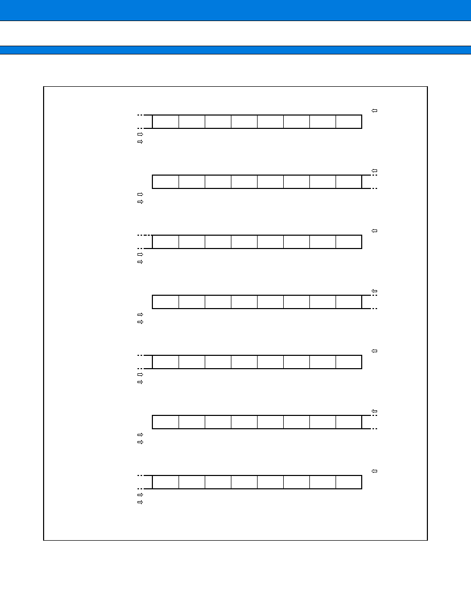
MB91360G Series
148
(2) Registers
PWM Control 0 register (PWC0)
Zero Detect 0 register (ZPD0)
PWM1 Compare 0 register (PWC10)
PWM2 Compare 0 register (PWC20)
PWM1 Select register (PWS10)
PWM2 Select register (PWS20)
PWM Clock Disable register (SMDBL0)
Bit no.
Address : 0000D1
H
Read/write
Default value
Bit no.
Address : 0000D0
H
Read/write
Default value
Bit no.
Address : 0000D9
H
Read/write
Default value
Bit no.
Address : 0000D8
H
Read/write
Default value
Bit no.
Address : 0000DB
H
Read/write
Default value
Bit no.
Address : 0000DA
H
Read/write
Default value
Bit no.
Address : 0000E8
H
Read/write
Default value
(
)
(
)
(R/W)
( 0 )
(R/W)
( 0 )
(R/W)
( 0 )
(
)
(
)
(
)
(
)
(R/W)
( 0 )
7
6
5
4
3
2
1
0
(
)
(
)
P1
P0
CE
TST
(R/W)
( 0 )
(R/W)
( 0 )
(R/W)
( 0 )
(R/W)
( 0 )
(R/W)
( 0 )
(R/W)
( 1 )
(R/W)
( 0 )
15
14
13
12
11
10
9
8
S0
(R/W)
( 0 )
S1
TS
T2
T1
T0
PD
RS
(R/W)
( X )
(R/W)
( X )
(R/W)
( X )
(R/W)
( X )
(R/W)
( X )
(R/W)
( X )
(R/W)
( X )
7
6
5
4
3
2
1
0
D6
(R/W)
( X )
D7
D5
D4
D3
D2
D1
D0
(R/W)
( X )
(R/W)
( X )
(R/W)
( X )
(R/W)
( X )
(R/W)
( X )
(R/W)
( X )
(R/W)
( X )
15
14
13
12
11
10
9
8
D6
(R/W)
( X )
D7
D5
D4
D3
D2
D1
D0
(
)
(
)
(R/W)
( 0 )
(R/W)
( 0 )
(R/W)
( 0 )
(R/W)
( 0 )
(R/W)
( 0 )
(R/W)
( 0 )
7
6
5
4
3
2
1
0
(
)
(
)
P2
P1
P0
M2
M1
M0
(R/W)
( 0 )
(R/W)
( 0 )
(R/W)
( 0 )
(R/W)
( 0 )
(R/W)
( 0 )
(R/W)
( 0 )
(R/W)
( 0 )
15
14
13
12
11
10
9
8
BS
(
)
(
)
P2
P1
P0
M2
M1
M0
(
)
(
)
(
)
(
)
(
)
(
)
(
)
(
)
(
)
(
)
(
)
(
)
(R/W)
( 0 )
7
6
5
4
3
2
1
0
(
)
(
)
DBL
MB91360G Series
149
27. REAL TIME CLOCK
This section provides an overview of the Real Time Clock (also called WatchTimer) , describes the register
structure and functions.The Real Time Clock (Watch Timer) consists of the Timer Control register, Sub-second
register, Second/Minute/Hour registers, 1/2 clock divider, 21bit prescaler and Second/Minute/Hour counters.
The Real Time Clock operates as the real-world timer and provides the real-world time information.
(1) Block Diagram
INTE0 INT0
EN
CI
EN
LOAD
CO
CO
WOT
IRQ
CO
CO
INTE1
ST
UPDT
INT1
INTE2 INT2
INT3
INT3
Oscillation
clock
1/2 Clock
Divider
21 bit prescaler
Sub second
register
Second counter
Minute counter
Hour counter
6 bits
6 bits
5 bits
Second/Minute/Hour register
MB91360G Series
150
(2) Registers
(Continued)
Timer disable register (WTDBL)
Timer control register (WTCR)
Sub-second register (WTBR)
Second register (WTSR)
Bit no.
Address : 0000F5
H
Read/write
Default value
Bit no.
Address : 0000F7
H
Read/write
Default value
Bit no.
Address : 0000F6
H
Read/write
Default value
Bit no.
Address : 0000FB
H
Read/write
Default value
Bit no.
Address : 0000FA
H
Read/write
Default value
Bit no.
Address : 0000F9
H
Read/write
Default value
Bit no.
Address : 0000FE
H
Read/write
Default value
(
)
(
)
(
)
(
)
(
)
(
)
(
)
(
)
(
)
(
)
(
)
(
)
(R/W)
( 0 )
7
6
5
4
3
2
1
0
(
)
(
)
DBL
(R/W)
( 0 )
(R/W)
( 0 )
(
)
(
)
( R )
( 0 )
(R/W)
( 0 )
(
)
(
)
(R/W)
( 0 )
7
6
5
4
3
2
1
0
TST1
(R/W)
( 0 )
TST2
TST0
RUN
UPDT
ST
(R/W)
( 0 )
(R/W)
( 0 )
(R/W)
( 0 )
(R/W)
( 0 )
(R/W)
( 0 )
(R/W)
( 0 )
(R/W)
( 0 )
15
14
13
12
11
10
9
8
INT3
(R/W)
( 0 )
INTE3
INTE2
INT2
INTE1
INT1
INTE0
INT0
(R/W)
( X )
(R/W)
( X )
(R/W)
( X )
(R/W)
( X )
(R/W)
( X )
(R/W)
( X )
(R/W)
( X )
7
6
5
4
3
2
1
0
D6
(R/W)
( X )
D7
D5
D4
D3
D2
D1
D0
(R/W)
( X )
(R/W)
( X )
(R/W)
( X )
(R/W)
( X )
(R/W)
( X )
(R/W)
( X )
(R/W)
( X )
15
14
13
12
11
10
9
8
D14
(R/W)
( X )
D15
D13
D12
D11
D10
D9
D8
(
)
(
)
(
)
(
)
(R/W)
( X )
(R/W)
( X )
(R/W)
( X )
(R/W)
( X )
(R/W)
( X )
7
6
5
4
3
2
1
0
(
)
(
)
D20
D19
D18
D17
D16
(
)
(
)
(R/W)
( X )
(R/W)
( X )
(R/W)
( X )
(R/W)
( X )
(R/W)
( X )
(R/W)
( X )
15
14
13
12
11
10
9
8
(
)
(
)
S5
S4
S3
S2
S1
S0
MB91360G Series
151
(Continued)
Minute register (WTMR)
Hour register (WTHR)
Bit no.
Address : 0000FD
H
Read/write
Default value
Bit no.
Address : 0000FC
H
Read/write
Default value
(
)
(
)
(R/W)
( X )
(R/W)
( X )
(R/W)
( X )
(R/W)
( X )
(R/W)
( X )
(R/W)
( X )
7
6
5
4
3
2
1
0
(
)
(
)
M5
M4
M3
M2
M1
M0
(
)
(
)
(
)
(
)
(R/W)
( X )
(R/W)
( X )
(R/W)
( X )
(R/W)
( X )
(R/W)
( X )
15
14
13
12
11
10
9
8
(
)
(
)
H4
H3
H2
H1
H0
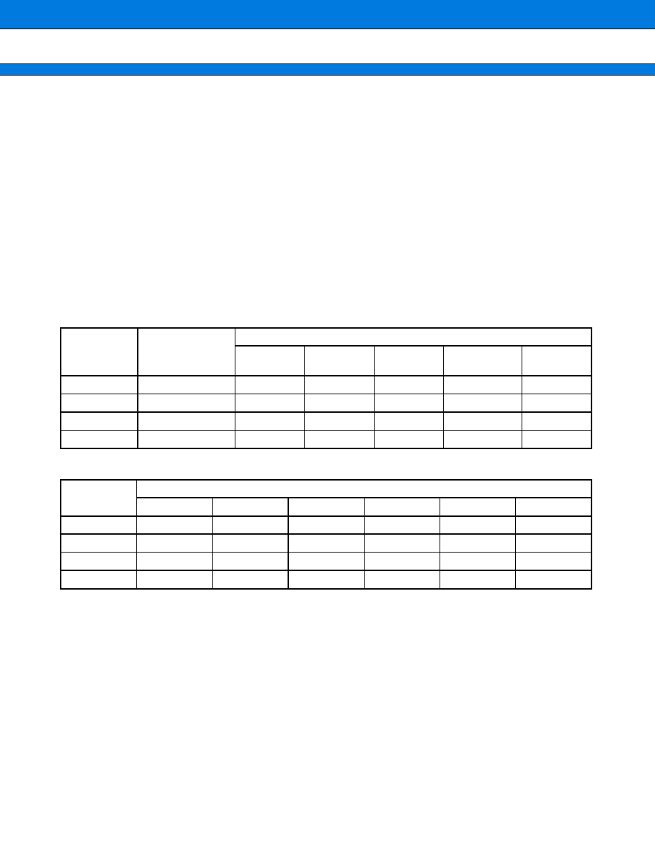
MB91360G Series
152
28. SUBCLOCK
The Subclock System provides various power saving modes. The key of the concept is to supply the 32 kHz
clock signal only to the Real Time Clock RTC) Module, while the rest of the MCU is provided with 4 MHz clock
signal in order to achieve lower power supply current in the RTC32K mode.
This behavior can be altered by the configuration input, SELCLK pin to switch the RTC module to operate with
the 4 MHz clock. The following sections describe the operation with SELCLK connected to "0" and SELCLK
connected to "1" respectively.
Note : On MB91F361GA and MB91F362GA SELCLK should always be connected to "1", subclock operation is not
implemented on those devices.
(1) Operation of Subclock (SELCLK
=
=
=
=
0)
The next table summarizes the operation states of the components related to the Subclock System.To simplify
this table SLEEP modes are not listed but the operation is the same as for RUN modes except that the CPU is
stopped.
The following table summarizes those operation modes and necessary software settings.
It is recommended that PLL2EN is set to "1" after the initialization to start the 32 kHz oscillation and this bit
should be kept at "1" during the operation. Otherwise the 32 kHz oscillator does not start. Also bits 9 and 10 of
the CLKR register (address 0046H) should always be set to "0" during operation.
Mode
Power dissipation
Operation of components
4 M Osc.
32 K Osc.
RTC
CPU &
Peripheral
PLL
RUN
High
Run
Run
Run
Run
Stop/Run
RTC4M32K
Medium Low
Run
Run
Run
Stop
Stop
RTC32K
Low
Stop
Run
Run
Stop
Stop
STOP
Lowest
Stop
Stop
Stop
Stop
Stop
Mode
Software Setting
STOP
PLL1EN
PLL2EN
OSCD1
OSCD2
RTC32
RUN
0
0 or 1
1
Don't Care
Don't Care
Don't Care
RTC4M32K
1
Don't Care
1
0
0
Don't Care
RTC32K
1
Don't Care
1
1
0
1
STOP
1
Don't Care
Don't Care
1
1
Don't Care
MB91360G Series
153
(2) 4 MHz Real Time Clock Configuration (SELCLK
=
=
=
=
1)
When the SELCLK pad is connected logic level 1, the 32 kHz oscillation is disabled regardless of the software
setting. In this configuration, the Real Time Clock Module is supplied with the 4 MHz oscillation clock signal.
The following table summaries the modes available in this configuration.
(3) Use of Real Time Clock Module
There is some additional consideration needed to operate the RTC module to achieve the desired functionality.
Because the RTC module is directly connected to the 32 kHz oscillation clock, the oscillation stabilization time
has to be taken care of by the software.This can be achieved by using another timer (e.g the Time Base Timer)
to trigger the software to start the RTC module (Setting of ST bit to "1") .
It is also important to stop the RTC module before entering the STOP mode. Otherwise, the reactivation from
STOP mode results in unpredictable operation of the RTC module.
After the reactivation, the oscillation stabilization time has to be measured again by the software, then the RTC
module can be restarted.
Mode
Power dissipation
Operation of components
4 M Osc.
32 K Osc.
RTC
CPU &
Peripheral
PLL
RUN
High
Run
Stop
Run
Run
Stop/Run
RTC4M
Medium Low
Run
Stop
Run
Stop
Stop
STOP
Lowest
Stop
Stop
Stop
Stop
Stop
Mode
Software Setting
STOP
PLL1EN
PLL2EN
OSCD1
OSCD2
RTC32
RUN
0
0 or 1
Don't Care
Don't Care
Don't Care
Don't Care
RTC4M
1
Don't Care
Don't Care
0
Don't Care
Don't Care
STOP
1
Don't Care
Don't Care
1
Don't Care
Don't Care
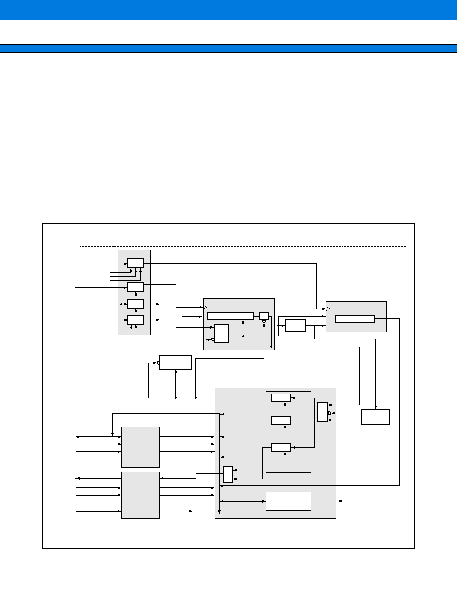
MB91360G Series
154
29. 32 kHz CLOCK CALIBRATION UNIT
The 32 kHz Clock Calibration Module provides possibilities to calibrate the 32 kHz oscillation clock with respect
to the 4 MHz oscillation clock.
(1) Description
This hardware allows the software to measure time generated by the 32 kHz clock with the 4 MHz clock.
By utilizing this hardware in conjunction with software processing, the accuracy of the 32 kHz clock can come
closer to that of the 4 MHz clock. The measurement result from the 32 kHz Clock Calibration Module can be
processed by the software and the setting required for the Real Time Clock Module can be obtained.
This module consists of two timers, one operating with the 32 kHz clock and the other operating with the 4 MHz
clock. The 32 kHz timer triggers the 4 MHz timer and resulting 4 MHz timer value is stored in a register. The
value stored in this register can be used for the subsequent software processing to calculate the desired Real
Time Clock module's setting.
(2) Block Diagram
UC18CLK
gate
gate
gate
gate
sync
CLKP
32
STRT
READY
RUNS
STRT
RSLEEPB
RSLEEPB
STRT
SLKPG2
=
CLKP
|
(
STRT & RSLEEPB)
;
OSC4
OSC32
CLKP
RB
RSLEEP
RMW
INT
*_RD
*_WR
RST
async
RST
STRT
STRTS
STRT
READY
RUN
UC18TRD
UC18TRR
CUTR
counter (16 bit)
CUTR (24 bit)
STRT
CUTD
CLK32G
RB
CLKPG
CLK4G
=
OSC4
|
STRT
|
(READY &
-
RUNS) ;
CLK4G
CLKPG2
32 kHz
TIMER
4 MHz
TIMER
anync
RST
sync
32
4
RUN
&
RUNS
sync
4
CLKP
READY
RUNSS1
RUNSS
&
reset
READY-
PULSE
CUCR (3 bit)
CUTR (24 bit)
CUTD (16 bit)
CUTD
VC18RBI
FC18
reset
set
STRT
set
/reset
set
/reset
INTEN
INT
UC18BUS
UC18IO
INT_I
INT_INT
*_RDB
*_WRB
RSTB
&
RBB
RSLEEPB
RMWB
MB91360G Series
155
(3) Timing
32 kHz
STRT (CLKP)
STRTS (32 kHz)
RUN (32 kHz)
RUNS (4 MHz)
32 kHz counter (16 bit)
4 MHz counter (24 bit)
READY (32 kHz)
READYPULSE (CLKP)
INT (CLKP)
new CUTR
old CUTR
CUTD
CUTD
CUTD-1
2
1
0
0
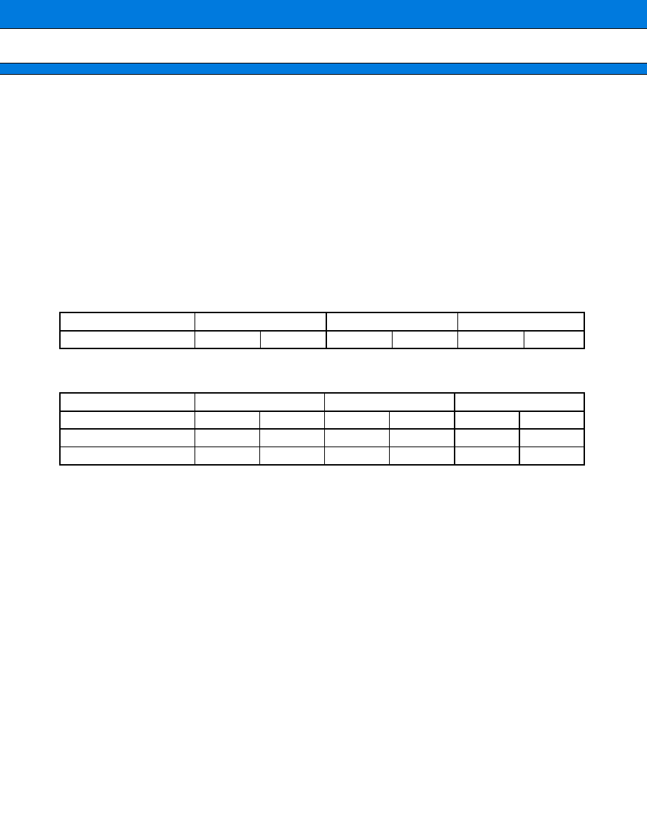
MB91360G Series
156
(4) Clocks
The module operates with 3 different clocks : The 4 MHz clock OSC4, the 32 kHz clock OSC32 and the Rbus
clock CLKP. Synchronization circuits adapt the different domains.
All 3 clocks are gated. The 32 kHz and the 4 MHz clock are switched off if STRT is 0. CLKPG is gated by RSLEEP
and CLKPG2 by RSLEEP and STRT for the 2 bits, which are set/reset by hardware.
The clock frequencies have to fulfill the following requirements :
1.) Clock ratio
T
OSC32
>
2
◊
T
OSC4
+
3
◊
T
CLKP
T
OSC4
<
1
/
2
◊
T
OSC32
-
3
/
2
◊
T
CLKP
T
CLKP
<
1
/
3
◊
T
OSC32
-
2
/
3
◊
T
OSC4
2.) The input frequencies must not exceed the values given in next table.
Maximum operation frequencies
Examples of valid clock ratios which fulfill requirements 1 and 2
CLKP
OSC32
OSC4
maximum
32 MHz
31.25 ns
4 MHz
250 ns
13 MHz
76.9 ns
OSC32
OSC4
CLKP
maximum operation speed
4 MHz
250 ns
13 MHz
76.9 ns
32 MHz
31.25 ns
standard TDIR mode
500 kHz
2000 ns
4 MHz
250 ns
4 MHz
250 ns
normal operation
32 kHz
31.25 us
4 MHz
250 ns
>
2 MHz
500 ns
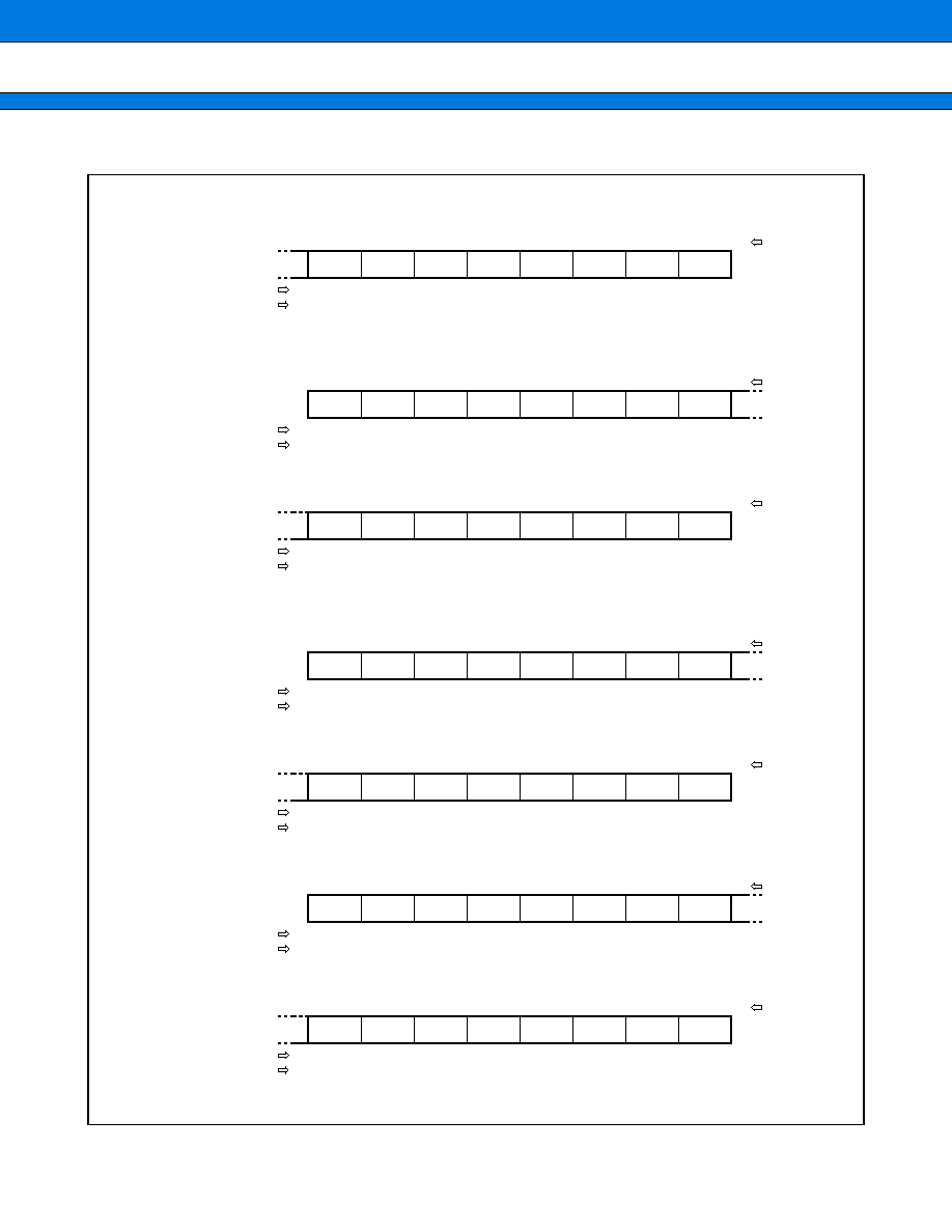
MB91360G Series
157
(5) Register Description
a : Calibration Unit Control Register (CUCR)
Control Register low byte (CUCRL)
b : 32 kHz Timer Data Register (CUTD)
32 kHz Timer Data Register high byte (CUTDH)
32 kHz Timer Data Register low byte (CUTDL)
c : 4 MHz Timer Data Register (CUTR)
4 MHz Timer Data Register1 high byte (CUTR1H)
4 MHz Timer Data Register1 low byte (CUTR1L)
4 MHz Timer Data Register2 high byte (CUTR2H)
4 MHz Timer Data Register2 low byte (CUTR2L)
Bit no.
Address : 000191
H
Read/write
Default value
Bit no.
Address : 000192
H
Read/write
Default value
Bit no.
Address : 000193
H
Read/write
Default value
Bit no.
Address : 000194
H
Read/write
Default value
Bit no.
Address : 000195
H
Read/write
Default value
Bit no.
Address : 000196
H
Read/write
Default value
Bit no.
Address : 000197
H
Read/write
Default value
( R )
( 0 )
( R )
( 0 )
(R/W)
( 0 )
( R )
( 0 )
(R/W)
( 0 )
(R/W)
( 0 )
(R/W)
( 0 )
7
6
5
4
3
2
1
0
( R )
( 0 )
STRT
INT
INTEN
(R/W)
( 0 )
(R/W)
( 0 )
(R/W)
( 0 )
(R/W)
( 0 )
(R/W)
( 0 )
(R/W)
( 0 )
(R/W)
( 0 )
15
14
13
12
11
10
9
8
TDD14
(R/W)
( 1 )
TDD15
TDD13
TDD12
TDD11
TDD10
TDD9
TDD8
(R/W)
( 0 )
(R/W)
( 0 )
(R/W)
( 0 )
(R/W)
( 0 )
(R/W)
( 0 )
(R/W)
( 0 )
(R/W)
( 0 )
7
6
5
4
3
2
1
0
TDD6
(R/W)
( 0 )
TDD7
TDD5
TDD4
TDD3
TDD2
TDD1
TDD0
( R )
( 0 )
( R )
( 0 )
( R )
( 0 )
( R )
( 0 )
( R )
( 0 )
( R )
( 0 )
( R )
( 0 )
15
14
13
12
11
10
9
8
( R )
( 0 )
( R )
( 0 )
( R )
( 0 )
( R )
( 0 )
( R )
( 0 )
( R )
( 0 )
( R )
( 0 )
( R )
( 0 )
7
6
5
4
3
2
1
0
TDR22
( R )
( 0 )
TDR23
TDR21
TDR20
TD19
TDR18
TDR17
TDR16
( R )
( 0 )
( R )
( 0 )
( R )
( 0 )
( R )
( 0 )
( R )
( 0 )
( R )
( 0 )
( R )
( 0 )
15
14
13
12
11
10
9
8
TDR14
( R )
( 0 )
TDR15
TDR13
TDR12
TDR11
TDR10
TDR9
TDR8
( R )
( 0 )
( R )
( 0 )
( R )
( 0 )
( R )
( 0 )
( R )
( 0 )
( R )
( 0 )
( R )
( 0 )
7
6
5
4
3
2
1
0
TDR6
( R )
( 0 )
TDR7
TDR5
TDR4
TD3
TDR2
TDR1
TDR0

MB91360G Series
158
30. FLASH MEMORY
MB91360G series devices feature 512 K of embedded flash memory unit derived from the MB29LV400C and
the FLASH Memory interface circuit.
(1) Out Line of Flash Memory
The Flash Memory consists of a flash memory unit derived from the MBM29LV400C and a flash memory interface
circuit.
Flash Memory :
∑ 512 Kword
◊
8 bit/256 Kword
◊
16 bit/128 Kword
◊
32 bit
(64 Kbyte
◊
3
+
32 Kbyte
+
8 Kbyte
◊
2
+
16 Kbyte) sectors
∑ Uses automatic program algorithm (Embedded Algorithm
TM
)
∑ Erase pause/restart function
∑ Detects completion of writing/erasing using data polling or toggle bit functions
∑ Detects completion of writing/erasing by RY/BY pin
∑ Compatible with JEDEC standard commands
∑ Performs minimum of 10,000 write/erase operations
∑ Sector erase function (any combination of sectors)
∑ Sector protect function
∑ Temporary sector protect cancellation function
∑ Allows flash memory interface circuit to write to/erase flash memory both under control of external pin by writer
and under control of internal bus by CPU.
Embedded Algorithm
TM
is a registered trademark of Advanced Micro Devices, Inc.
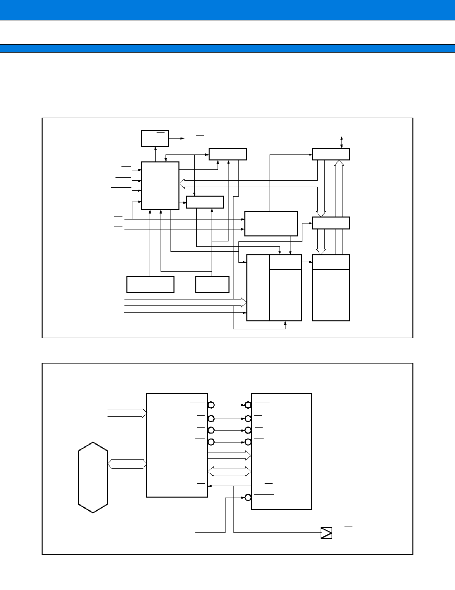
MB91360G Series
159
(2) Block diagrams of Flash Memory
a : Block diagram of Flash Memory
Figure shows the block diagram of the flash memory unit, which has almost the same configuration as the
MBM29LV400C.
b : Entire block diagram of Flash Memory
Figure shows the entire block diagram of the Flash Memory with the flash memory interface circuit.
WE
RY/BY
buffer
CE
A0 to A17
A-1
OE
BYTE
RESET
RY/BY
Erase circuit
Write circuit
Control
circuit
Chip enable/
output enable
circuit
I/O buffer
Data latch
Y gate
Y decoder
cell matrix
X decoder
address
latch
STB
STB
DQ
0
to DQ
15
Low V
CC
detection circuit
Write/erase
pulse timer
User
Logic
bus
Ext.Bus
I/F
Flash memorry
interface circuit
4 Mbit flash memory
BYTE
CE
OE
WE
A0 to A18
DQ0 to DQ15
RY/BY
BYTE
CE
OE
WE
A0 to A17
A-1
DQ0 to DQ15
RY/BY
RESET
External reset signal
RY/BY
write enable signal
MB91360G Series
160
c : Sector configuration
i) write, byte read, half word read
ii) long word read
Flash Memory mode
Other modes
8 bit
◊
2
7FFFF
H
FFFFF
H
Sector 13
16 KB
7C000
H
FC000
H
Sector 12
8 KB
7A000
H
FA000
H
Sector 11
8 KB
78000
H
F8000
H
Sector 10
32 KB
70000
H
F0000
H
Sector 9
64 KB
60000
H
E0000
H
Sector 8
64 KB
50000
H
D0000
H
Sector 7
64 KB
40000
H
C0000
H
Sector 6
16 KB
3C000
H
BC000
H
Sector 5
8 KB
3A000
H
BA000
H
Sector4
8 KB
38000
H
B8000
H
Sector 3
32 KB
30000
H
B0000
H
Sector 2
64 KB
20000
H
A0000
H
Sector 1
64 KB
10000
H
90000
H
Sector 0
64 KB
00000
H
80000
H
MSB
LSB
Flash Memory
mode
Other modes
8 bit
◊
2
8 bit
◊
2
7FFFF
H
FFFFF
H
Sector 13
16 KB
Sector 6
16 KB
78000
H
F8000
H
Sector 12
8 KB
Sector 5
8 KB
74000
H
F4000
H
Sector 11
8 KB
Sector 4
8 KB
70000
H
F0000
H
Sector 10
32 KB
Sector 3
32 KB
60000
H
E0000
H
Sector 9
64 KB
Sector 2
64 KB
40000
H
C0000
H
Sector 8
64 KB
Sector 1
64 KB
20000
H
A0000
H
Sector 7
64 KB
Sector 0
64 KB
00000
H
80000
H

MB91360G Series
161
(3) Write/Erase Modes
The flash memory can be accessed in two different ways; the flash memory mode allowing write/erase directly
from the external pins, and the other modes allowing write/erase from the CPU via the internal bus. These modes
are selected by the external mode pins.
a : Flash Memory mode
The CPU stops when the mode pins are set to 111 while the INITX signal is asserted. The flash memory interface
circuit is directly connected to the external bus interface, allowing direct control by the external pins. This mode
makes the MCU seem like a standard flash memory at the external pins, and write/erase can be performed
using a flash memory programmer.
In the flash memory mode all the operations supported by the flash memory automatic algorithm can be used.
b : Other modes
The flash memory is located in the CS1X area of the CPU memory space and like ordinary mask ROM can be
read-accessed and program-accessed from the CPU through the flash memory interface circuit.
Writing/erasing the flash memory is performed by instructions from the CPU via the flash memory interface
circuit. Therefore, this mode allows rewriting even when the MCU is soldered on the target board.
The sector protect operations can not be performed in these modes.
c : Control signals of flash memory
Next table lists the flash memory control signals in the flash memory mode.
There is almost a one-to-one correspondence between the flash memory control signals and the external pins
of the MBM291V400TA. The V
ID
(12 V) pins required by the sector protect operations are MD0, MD1 and MD2
instead of A9, RESET and OE for the MBM29LV400C.
In the flash memory mode, the width of the external data bus can be 8 or 16 bit.
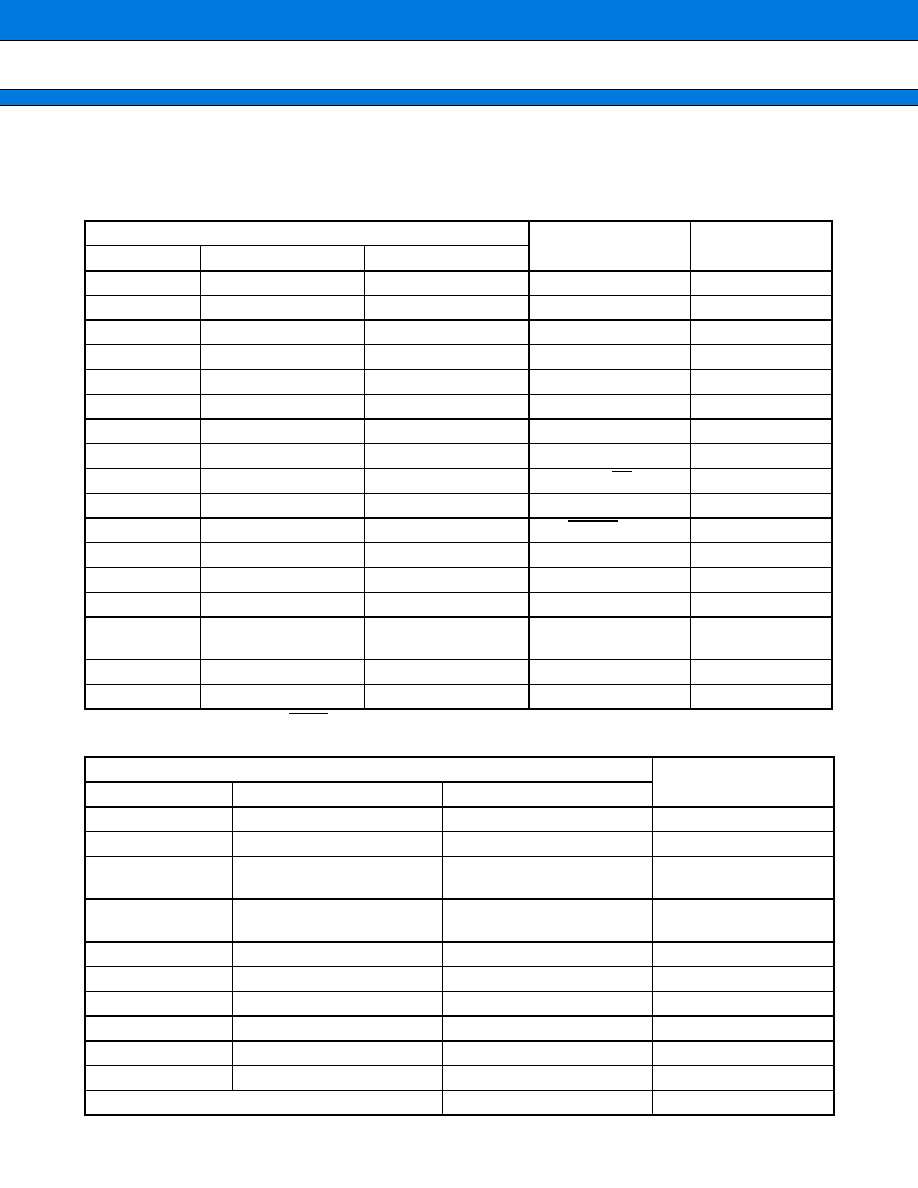
MB91360G Series
162
Flash Control Signals
∑
∑
∑
∑
MB91F362GA
Pins used in flash memory mode
A19, A20 should be pulled up, INITX must be low during power on for at least 500 ns.
Pins not used in flash memory mode
MB91F362GA
MBM29LV400C
Notes
Pin number
Normal function
Flash Memory mode
1 to 8
D24 to D31
D24 to D31
DQ8 to DQ15
9
A0
A0
A-1
10 to 24
A1 to A15
A1 to A15
A0 to A14
27 to 30
A16 to A18
A16 to A18
A15 to A17
32
CS4X
CS4X
WE
33
CS5X
CS5X
BYTE
35
RDY
RDY
OE
36
BGRNTX
BGRNTX
CE
37
BRQ
BRQ
RY/BY
111
MD0
VDA9
A9 (V
ID
)
112
MD1
VDRS
RESET (V
ID
)
113
MD2
VDOE
OE (V
ID
)
115
INITX
INITX
RESET
201 to 208
D16 to D23
D16 to D23
DQ0 to DQ7
183 to 197,
200
D0 to D15
Output when reading
from flash
Pull up
34
CS6X
TMODEX
Must be pulled up
30 to 31
A19 to A20
A19 to A20
Pull up or pull down
MB91F362GA
Notes
Pin number
Normal function
Pin state
75 to 76
DA0, DA1
output
leave open
77
ALARM
input
pull down
81 to 83
TESTX, CPUTESTX,
LTESTX
input
pull up or leave open
(internal pull-up)
114
HSTX
input
pull up or leave open
(internal pull-up)
116
MONCLK
output
leave open
117
SELCLK
input
pull up
119, 121
X0, X0A
input
pull down
120, 122
X1, X1A
output
leave open
124
CPO
output
leave open
125
VCI
input
pull down
all other signals
input
Pull up
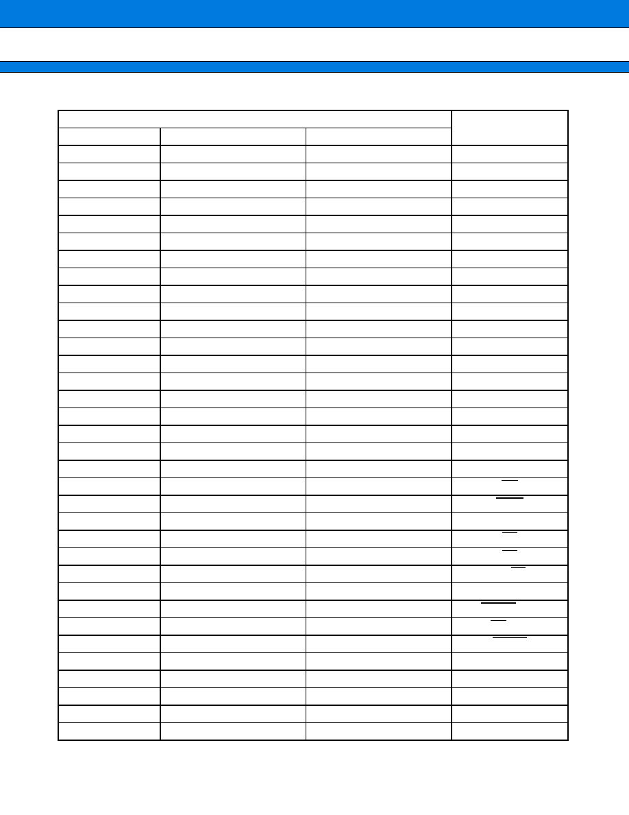
MB91360G Series
163
∑
∑
∑
∑
MB91FV360GA
(Continued)
MB91FV360GA
MBM29LV400C
Pin number
Normal function
Flash Memory mode
202
A0
A0
A-1
310
A1
A1
A0
201
A2
A2
A1
357
A3
A3
A2
257
A4
A4
A3
144
A5
A5
A4
309
A6
A6
A5
256
A7
A7
A6
200
A8
A8
A7
356
A9
A9
A8
308
A10
A10
A9
92
A11
A11
A10
44
A12
A12
A11
255
A13
A13
A12
143
A14
A14
A13
199
A15
A15
A14
307
A16
A16
A15
91
A17
A17
A16
142
A18
A18
A17
140
CS4X
CS4X
WE
196
CS5X
CS5X
BYTE
89
CS6X
TMODX
305
RDY
RDY
OE
139
BGRNTX
BGRNTX
CE
88
BRQ
BRQ
RY/BY
293
MD0
VDA9
A9 (V
ID
)
31
MD1
VDRS
RESET (V
ID
)
239
MD2
VDOE
OE (V
ID
)
30
INITX
INITX
RESET
46
D16
D16
DQ0
95
D17
D17
DQ1
1
D18
D18
DQ2
148
D19
D19
DQ3
205
D20
D20
DQ4
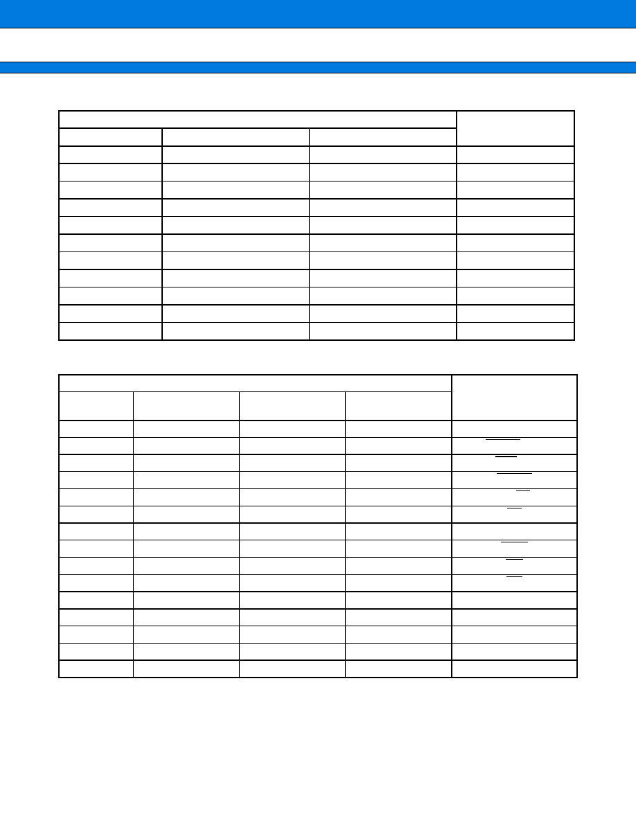
MB91360G Series
164
(Continued)
∑
∑
∑
∑
MB91F369GA
a. Pin 70 must be pulled high in Flash Memory Mode.
b. Pins 74 and 75 must be pulled low in Flash Memory Mode.
c. Functionality as described in the Data Sheet of MBM29LV400C.
AVRH must be tight to a high level, ALARM to a low level. All other Pins can be left open during Flash Memory
Mode.
MB91FV360GA
MBM29LV400C
Pin number
Normal function
Flash Memory mode
45
D21
D21
DQ5
94
D22
D22
DQ6
260
D23
D23
DQ7
312
D24
D24
DQ8
204
D25
D25
DQ9
147
D26
D26
DQ10
93
D27
D27
DQ11
259
D28
D28
DQ12
203
D29
D29
DQ13
146
D30
D30
DQ14
258
D31
D31
DQ15
MB91F369GA
MBM29LV400C
Pin number
Normal function
Flash Memory mode
Function in Flash
Memory mode
58
MD0
HVDA9
High Volt. A9
(C)
A9 (V
ID
)
59
MD1
HVDR5
High Volt. RESET
(C)
RESET (V
ID
)
60
MD2
HVDOE
High Volt. OE
(C)
OE (V
ID
)
62
INTX
RSTX
Hardware Reset
RESET
68
INT0
RY/BYX
Ready/Busy
RY/BY
69
INT1
CEX
Chip Enable
CE
70
INT2
TSTX
(a)
Flash Test
71
INT3
BYTEX
switch 8/16 bit mode
BYTE
72
INT4
WEX
Write Enable
WE
73
INT5
OEX
Output Enable
OE
74
INT6
ATDIN
(b)
Access signal ATD
75
INT7
EQIN
(b)
Access signal EQ
121 to 136
D0 to D15
AQ19 downto AQ4
Address input
A19 downto A4
139 to 154
D16 to D31
DQ16 to DQ31
Data input/output
DQ0 to DQ15
157 to 160
A0 to A3
AQ0 to AQ3
Address input
A0 to A3
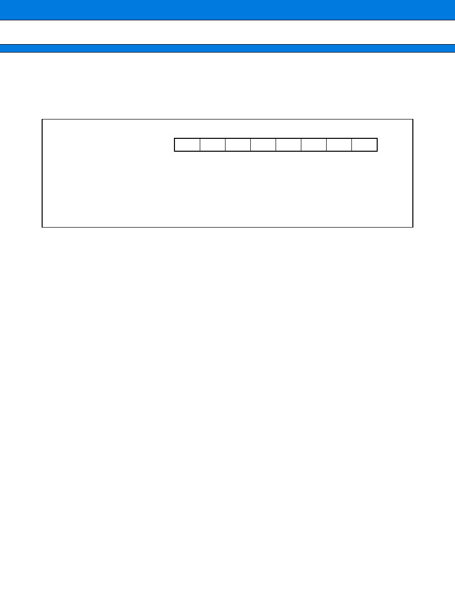
MB91360G Series
165
(4) Flash Control Status Register (FMCS)
Flash Memory Macros used in devices :
Normal Flash Macro used in : MB91F362GA
Fast Flash Macro used in : MB91FV360GA
*: It is not allowed to use RDYEG.
Address
FV360GA, F362GA :
00007000
H
Access
Initial value
value after
Boot ROM
R/W
1
1
R/W
1
1
R
0
0
R
X
X
R/W
0
0
R/W
0
0
R/W
0
0
bit 7
bit 6
bit 5
bit 4
bit 3
bit 2
bit 1
bit 0
R/W
1
0
FACCEN
RDYEG*
RDY
RDYI
WE
LPM
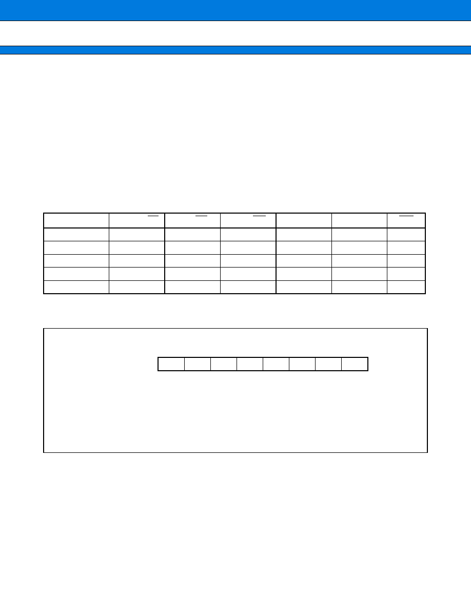
MB91360G Series
166
(5) Read/Write Access
In the flash memory mode, read/write access to the flash memory must be under control of the external pins.
However, with the CPU access, there are no special timing constraints on read/write access because the flash
memory is controlled by the flash memory interface circuit.
In this section, "write access" does not directly mean "program flash memory". It implies "activation of the flash
commands".
a : Read/write access in flash memory mode
Next table gives the setting of pins for read/write access in the Flash Memory mode. There is no special problem
with control of these pins if connected to a flash memory writer. However, in other cases, timing specifications
must be met.
Setting Conditions of Pins for Read/Write Access in Flash Memory Mode
Note : This table uses pin names from F362GA. Check corresponding pin names of other devices.
b : Read access with CPU
Operations
BGRNTX (CE) RDY
(OE)
CS4X (WE)
A0 to A18
D16 to D31
INIT
Read
L
L
H
Read address
D
OUT
H
Write
L
H
L
Write address
D
IN
H
Output disable
L
H
H
x
High-Z
H
Standby
H
x
x
x
High-Z
H
Hardware reset
x
x
x
x
High-Z
L
Flash Wait Control Register (FMWT)
Address
00007004
H
Access
Initial value
value after Boot ROM
Normal Flash Macro
value after Boot ROM
Fast Flash Macro
R/W
0
0
0
R/W
0
0
0
R/W
0
0
1
R/W
0
0
0
R/W
0
0
0
R/W
1
1
1
R/W
1
1
1
bit 7
bit 6
bit 5
bit 4
bit 3
bit 2
bit 1
bit 0
FAC1
FAC0
EQINH
WTC2
WTC1
WTC0
MB91360G Series
167
Normal Flash Macro : Recommended settings
Without applying clock modulation
When applying clock modulation
Example for flash memory read access with 1 cycle for the low time of FACC and 3 wait cycles
The minimum value for t
FP
is 15 ns, for t
FACC
it is 40 ns.
CLKB unmodulated
core clock frequency
[MHz]
FAC1
FAC0
EQINH
WTC2
WTC1
WTC0
FACC low
cycles/wait
cycles
FMWT
64
0
1
0
0
1
1
1
/
3
13
H
48
0
1
0
0
1
1
1
/
3
13
H
40
0
1
0
0
1
0
1
/
2
12
H
32
0
0
0
0
1
0
0.5
/
2
02
H
24
0
0
0
0
0
1
0.5
/
1
01
H
16
0
0
0
0
0
1
0.5
/
1
01
H
CLKB core clock
frequency
[MHz]
Peak Max
frequency
FAC1
FAC0
EQINH WTC2
WTC1
WTC0
FACC low
cycles/wait
cycles
FMWT
48
64
0
1
0
0
1
1
1
/
3
13
H
32
48
0
1
0
0
1
1
1
/
3
13
H
24
40
0
1
0
0
1
0
1
/
2
12
H
24
32
0
0
0
0
1
0
0.5
/
2
02
H
16
24
0
0
0
0
0
1
0.5
/
1
01
H
A1
A2
A3
D1
CLKB
FA
FWAITR
FACC
FD
3 wait cycles
1 cycle
FACC = "L"
t
FP
t
FACC
core
clock
F-bus
address
F-bus
wait
FACC
for flash
F-bus
data
MB91360G Series
168
Fast Flash Macro : Recommended settings
Without applying clock modulation
When applying clock modulation
Example for flash memory read access with 1 cycle for the high time of ATDIN and 3 wait cycles
The minimum value for t
WATD
is 10 ns, the minimum value for t
WEQ
is 20 ns.
The minimum value for t
RC
is 40 ns.
The maximum value for t
ACC
is t
WATD
+
t
WEQ
+
5 ns.
CLKB unmodulated
core clock frequency
[MHz]
FAC1
FAC0
EQINH
WTC2
WTC1
WTC0
ATDIN high
cycles/wait
cycles
FMWT
64
0
1
0
0
1
1
1
/
3
13
H
48
0
0
0
0
1
0
0.5
/
2
02
H
40
0
0
0
0
1
0
0.5
/
2
02
H
32
0
0
1
0
0
1
0.5
/
1
09
H
24
0
0
0
0
0
1
0.5
/
1
01
H
16
0
0
0
0
0
1
0.5
/
1
01
H
CLKB core clock
frequency
[MHz]
Peak Max
frequency
FAC1
FAC0
EQINH
WTC2
WTC1
WTC0
ATDIN high
cycles/wait
cycles
FMWT
48
64
0
1
0
0
1
1
1
/
3
13
H
32
48
0
0
0
0
1
0
0.5
/
2
02
H
24
40
0
0
0
0
1
0
0.5
/
2
12
H
24
32
0
0
1
0
0
1
0.5
/
1
09
H
16
24
0
0
0
0
0
1
0.5
/
1
01
H
3 wait cycles
1 cycle
ATDIN ="H"
A1
D1
A2
A3
t
WATD
t
WEQ
core
clock
F-bus
address
F-bus
wait
ATDIN
for flash
EQIN
for flash
F-bus
data
t
ACC
t
RC
CLKB
FA
FWAITR
ATDIN
EQIN
FD
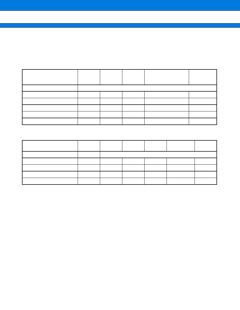
MB91360G Series
169
c : Write access with CPU
Recommended settings for WTC2 to WTC0 for write access to the flash memory, FACCEN of FMCS should be
set to 1 for writing, so FAC1, FAC0, EQINH register settings then have no meaning for the write operation
Without applying clock modulation
When applying clock modulation
CLKB unmodulated
core clock frequency
[MHz]
WTC2
WTC1
WTC0
Wait cycles
FMWT
64
setting not allowed for writing
48
1
0
0
4
X4
H
40
1
0
0
4
X4
H
32
0
1
0
2
X2
H
24
0
1
0
2
X2
H
16
0
0
1
1
X1
H
CLKB core clock
frequency [MHz]
Peak Max
frequency
WTC2
WTC1
WTC0
Wait cycles
FMWT
48
64
setting not allowed for writing
32
48
1
0
0
4
X4
H
24
40
1
0
0
4
X4
H
24
32
0
1
0
2
X2
H
16
24
0
1
0
2
X2
H
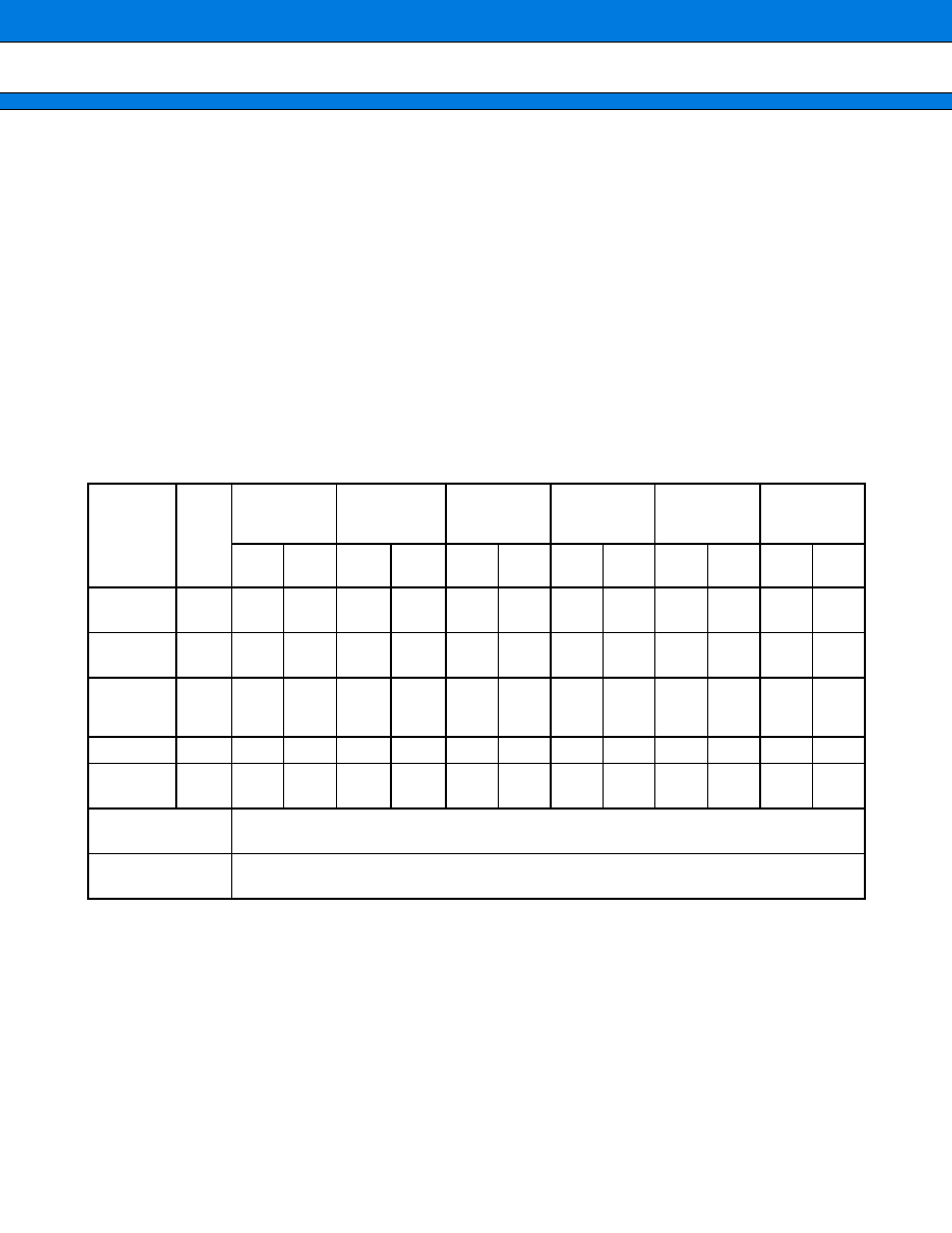
MB91360G Series
170
(6) Automatic Write/Erase
Irrespective of the Flash Memory mode or other modes, writing to/erasing the flash memory unit is performed
by starting the flash memory automatic algorithm.
To start the automatic algorithm, various sequences of write accesses are executed in 1 to 6 cycles. They are
called Flash commands.
a : Flash Commands
There are four commands for starting the automatic algorithm of the Flash Memory unit; Read/Reset, Write,
Chip Erase, and Sector Erase. There are also Erase Suspend and Erase Resume commands for the sector
erase operation.
Next tables give the command sequence lists in the flash memory and other modes.
b : Command sequence
Command Sequence List (CPU access)
Addresses in the table are the values in the CPU memory space. All addresses and data are hexadecimal values,
where x is any value and
**
may be 08 to 0F.
* : Two Read/Reset commands reset Flash memory to the read mode.
Command
Sequence
Write
Cycle
of
Bus
Write Cycle
of First Bus
Write Cycle of
Second Bus
Write Cycle
of Third Bus
Read/ Write
Cycle of
Fourth Bus
Write Cycle
of Fifth Bus
Write Cycle
of Sixth Bus
Ad-
dress
Data
Ad-
dress
Data
Ad-
dress
Data
Ad-
dress
Data
Ad-
dress
Data
Ad-
dress
Data
Read/
Reset*
1
**xxxx
xxF0
Read/
Reset*
4
**5554
xxAA
**aaa8
xx55
**5554
xxF0
RA
RD
Write
4
**5554
xxAA
**aaa8
xx55
**5554
xxA0
PA
(even)
PD
(half
word)
Chip Erase
6
**5554
xxAA
*
*
aaa8
xx55
**5554
xx80
**5554
xxAA
**aaa8
xx55
**5554
xx10
Sector
Erase
6
**5554
xxAA
**aaa8
xx55
**5554
xx80
**5554
xxAA
**aaa8
xx55
SA
(even)
xx30
Sector Erase
Suspend
Input of address
**
xxxx or data (xxB0
H
) suspends sector erasing.
Sector Erase
Resume
Input of address
**
xxxx or data (xx30
H
) suspends and resumes sector erasing.
MB91360G Series
171
Command Sequence List (Flash Memory Mode)
Addresses in the table are values for writer addresses. All addresses and data are hexadecimal values, where x
is any value and * may be 0 to 7.
RA : Read address
PA : Write address. Only even addresses can be specified.
SA : Sector address (See next table) . Only even addresses can be specified.
RD : Read data
PD : Write data. Only word data can be specified.
Command
Sequence
Write
Cycle
of
Bus
Write Cycle
of First Bus
Write Cycle
of Second
Bus
Write Cycle
of Third Bus
Read/ Write
Cycle of
Fourth Bus
Write Cycle
of Fifth Bus
Write Cycle
of Sixth Bus
Ad-
dress
Data
Ad-
dress
Data
Ad-
dress
Data
Ad-
dress
Data
Ad-
dress
Data
Ad-
dress
Data
Read/
Reset*
1
*
xxxx
F0
Read/
Reset*
4
*aaaa
AA
*5554
55
*aaaa
F0
RA
RD
Write
4
*
aaaa
AA
*5554
55
*
aaaa
A0
PA
(even)
PD
(word)
Chip Erase
6
*
aaaa
AA
*5554
55
*
aaaa
80
*
aaaa
AA
*5554
55
*
aaaa
10
Sector
Erase
6
*aaaa
AA
*5554
55
*aaaa
80
*aaaa
AA
*5554
55
SA
(even)
30
Sector Erase
Suspend
Input of address *xxxx or data (B0
H
) suspends sector erasing.
Sector Erase
Resume
Input of address *xxxx or data (30
H
) suspends and resumes sector erasing.
MB91360G Series
172
Sector Address for half word mode
Sector
A18
A17
A16
A15
A14
A13
Address range
SA13
1
1
1
1
1
7C000
H
to 7FFFF
H
SA12
1
1
1
1
0
1
7A000
H
to 7BFFF
H
SA11
1
1
1
1
0
0
78000
H
to 79FFF
SA10
1
1
1
0
70000
H
to 77FFF
H
SA9
1
1
0
60000
H
to 6FFFF
H
SA8
1
0
1
50000
H
to 5FFFF
H
SA7
1
0
0
40000
H
to 4FFFF
H
SA6
0
1
1
1
1
3C000
H
to 3FFFF
H
SA5
0
1
1
1
0
1
3A000
H
to 3BFFF
H
SA4
0
1
1
1
0
0
38000
H
to 39FFF
H
SA3
0
1
1
0
30000
H
to 37FFF
H
SA2
0
1
0
20000
H
to 2FFFF
H
SA1
0
0
1
10000
H
to 1FFFF
H
SA0
0
0
0
00000
H
to 0FFFF
H
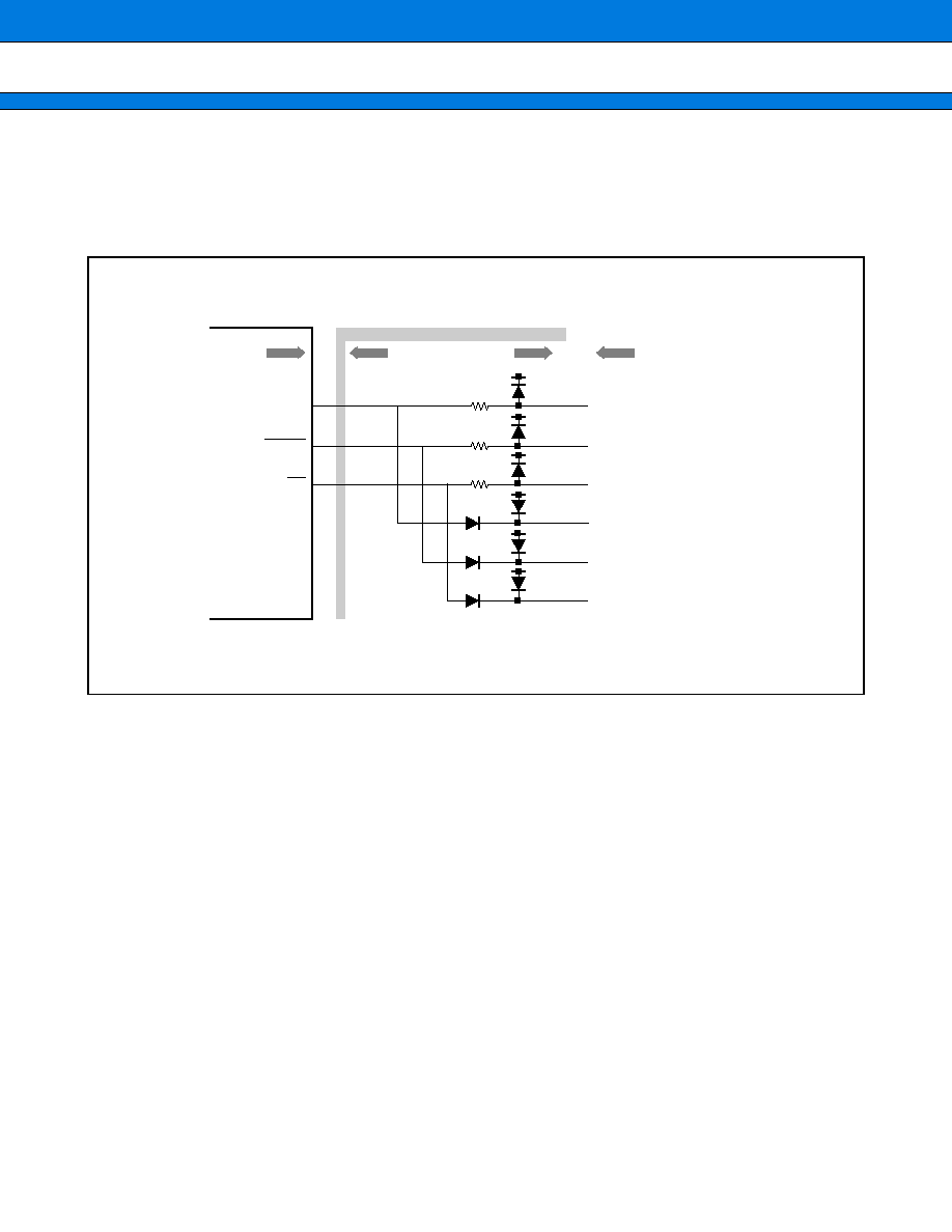
MB91360G Series
173
(7) Connection to Flash Memory
The Flash Memory mode of the MB91360G series devices is intended mainly for external connection to a flash
memory writer. As indicated in Table Flash Control Signals, there is a slight difference between the external pins
of the MB91360G series devices and the MBM29LV400C (4 Mbit flash memory) . Connection to an
MBM29LV400C writer requires the socket adapter.
flash writer
MB91F362GA
MB91FV360GA
2.2 k
2.2 k
2.2 k
2.2 k
2.2 k
2.2 k
Socket adapter
A9
RESET
OE
A10
INITX
RDY
MD0
MD1
MD2
MB91F369GA
D9
INITX
INT5
MD0
MD1
MD2

MB91360G Series
174
(8) Notes to Use of Flash Memory
Notes on the Flash Memory in MB91360G series devices are given below.
a : Input of hardware reset (INITX)
To input a hardware reset when the automatic algorithm is not started, where reading is in progress, a minimum
of 500 ns should be taken at a low-level width. In this case, a maximum of 500 ns is required until data can be
read from the flash memory after a hardware reset has been activated.
Similarly, to input a hardware reset when the automatic algorithm is activated, where writing/erasing is in
progress, a minimum of 50 ns should be taken in a low-level width. In this case, 20
µ
s are required until data
can be read after the executing operation has been terminated to initialize the flash memory.
A hardware reset during writing undefined data being written. A hardware reset during erasing may make the
sector being erased unusable.
b : Canceling software reset, watchdog timer reset, and hardware standby
When writing/erasing the flash memory with the CPU access and if reset conditions occur while the automatic
algorithm is active, the CPU may run away. This occurs because these reset conditions cause the automatic
algorithm to continue without initializing the flash memory unit, possibly preventing the flash memory unit from
entering the read state when the CPU starts the sequence after the reset has been deasserted. These reset
conditions should be inhibited during writing/erasing the Flash Memory.
c : Program access to Flash Memory
When the automatic algorithm is operating, read access to the flash memory is disabled. With the memory
access mode of the CPU set to the internal ROM mode, writing/erasing should be started after switching the
program area to another area such as RAM.
In this case, when sectors containing interrupt vectors are erased, interrupt processing cannot be executed.
For the same reason, all interrupt sources should be disabled while the automatic algorithm is operating.
d : Hold function
When the CPU accepts a hold request, the Write signal WE of the flash memory unit may be skewed and many
cause erroneous writing/erasing. When the acceptance of a hold request is enabled, ensure that the WE bit of
the control status register (FMCS) is 0.
e : Applying V
ID
Applying V
ID
required for the sector protect operation should always be started and terminated when the supply
voltage is on.
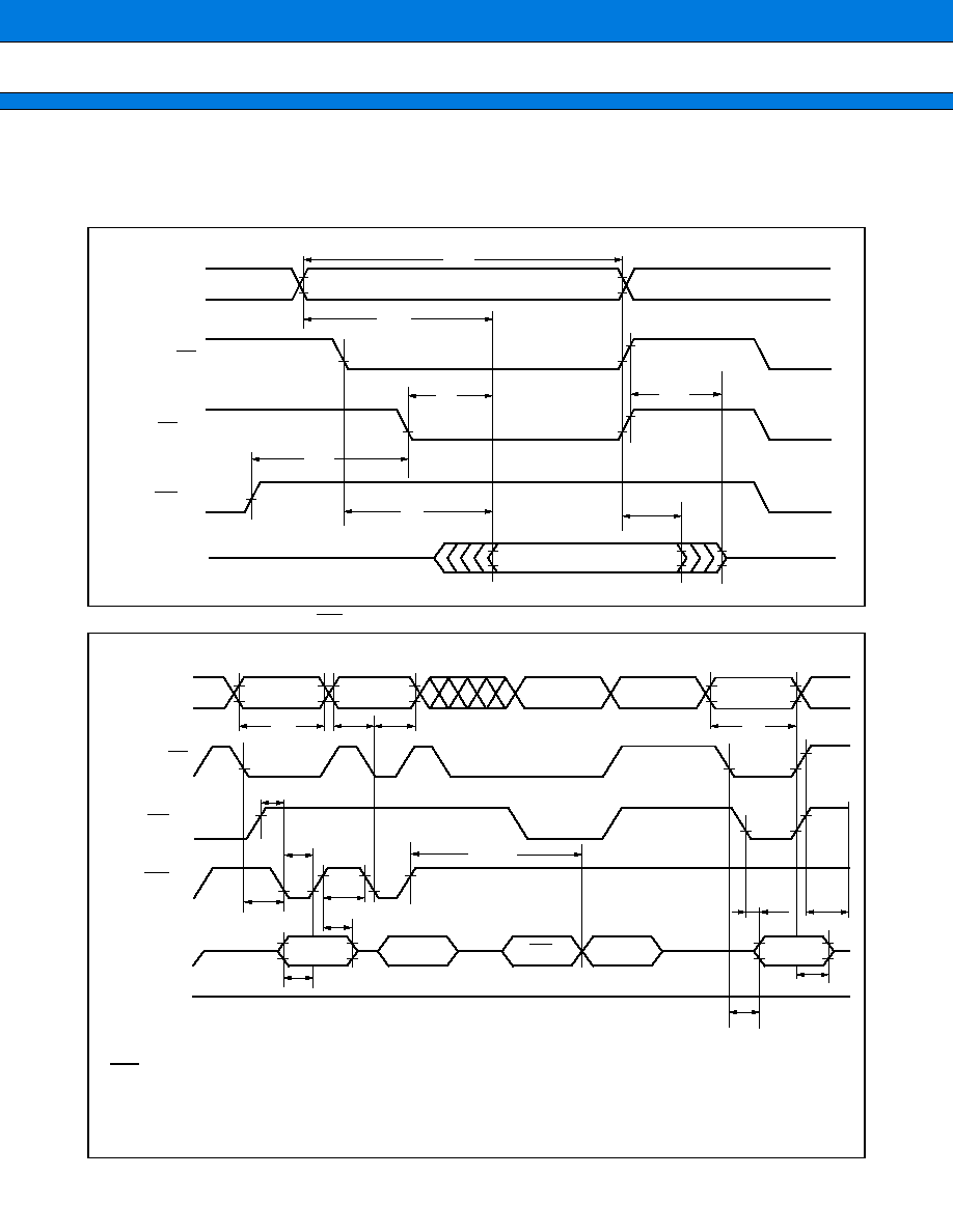
MB91360G Series
175
(9) Timing Diagrams in Flash Mode
Each timing diagram for the external pins of the MB91360G series in the Flash Memory mode is shown below.
a : Data read by read access
b : Write Data polling Read (WE control)
A18 to A0
Address stable
High-Z
High-Z
BGRNTX (CE)
RDY (OE)
CS4X (WE)
D31 to D16
Output defined
t
RC
t
AC
t
OE
t
DF
t
CE
t
OH
t
OEH
120 ns
120 ns
0
50 ns
30 ns
120 ns (TOGGLE)
0 ms (Read)
A18 to A0
D31 to D16
BGRNTX (CE)
RDY (OE)
CS4X (WE)
Third bus cycle
Data Polling
7AAAA
H
PA
PA
t
WC
t
AS
t
AH
t
RC
t
WHWH1
t
WPH
t
WP
t
GHEL
t
DH
t
DF
t
OH
t
OE
t
CS
t
DS
t
CE
D
OUT
D23
PD
A0
H
V
DD
(= 5.0 V)
PA : Write address
PD : Write data
D23 : Reverse output of write data
D
OUT
: Output of write data
Note : The last two bus cycle sequences out of the four are described.
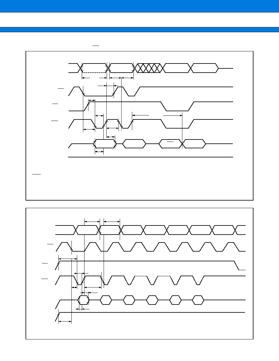
MB91360G Series
176
c : Write Data polling Read (CE control)
d : Chip erase/sector erase command sequence
A18 to A0
D31 to D16
BGRNTX (CE)
RDY (OE)
CS4X (WE)
V
DD
(= 5.0 V)
Third bus cycle
Data Polling
7AAAA
H
PA
PA
t
WC
t
AS
t
WH
t
AH
t
WHWH1
t
CPH
t
CP
t
GHEL
t
DH
t
WS
t
DS
D
OUT
D23
PD
A0
H
PA : Write address
PD : Write data
D23 : Reverse output of write data
D
OUT
: Output of write data
Note : The last two bus cycle sequences out of the four are described.
A18 to A0
D31 to D16
V
DD
BGRNTX (CE)
RDY (OE)
CS4X (WE)
7AAAA
H
75554
H
7AAAA
H
7AAAA
H
75554
H
SA*
t
AS
t
AH
t
WP
t
DS
t
CS
t
VCS
t
DH
t
WPH
AA
H
55
H
80
H
AA
H
55
H
10
H
/30
H
t
GHWL
Note : SA is the sector address at sector erasing. 7AAAA
H
(or 6AAAA
H
) is the address at chip erasing.
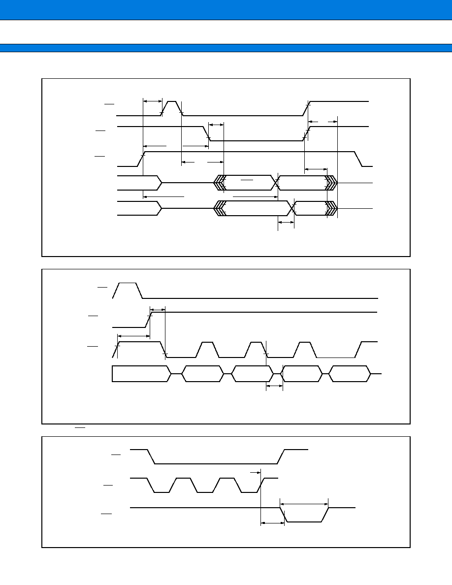
MB91360G Series
177
e : Data polling
f : Toggle bit
g : RY/BY timing during writing/erasing
t
OEH
t
CH
t
OE
t
CE
t
DF
t
EOE
t
OH
t
WHWH1 or
t
WHWH2
BGRNTX (CE)
D31 to D16
D23
D23
=
Valid data
D31 - D16
=
Invalid
D31 - D16 =
Valid data
RDY (OE)
CS4X (WE)
High-Z
D23
*
* : DQ7 is valid data (The device terminates automatic operation) .
t
OEH
t
OE
BGRNTX (CE)
RDY (OE)
CS4X (WE)
Data
(D31 to D16)
*
t
OES
D22
=
Toggle
D22
=
Toggle
D22
=
Stop
toggling
D31 to D16
=
Valid
*
* : DQ6 stops toggling (The device terminates automatic operation) .
BGRNTX (CE)
CS4X (WE)
RDY (OE)
Rising edge of last write pulse
t
BUSY
Writing or erasing
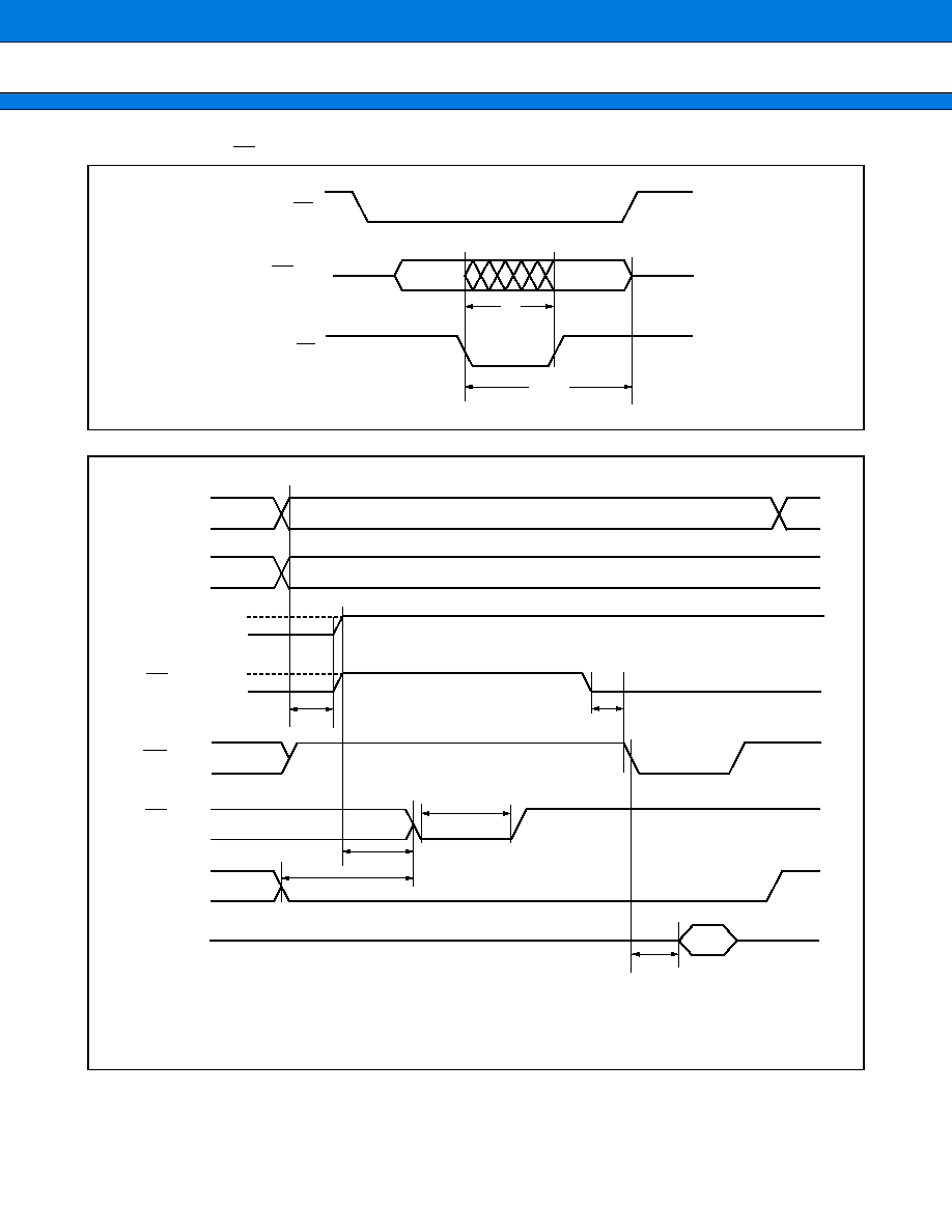
MB91360G Series
178
h : INITX and RY/BY timing
i : Enable sector protect/verify sector protect
t
RP
t
READY
BRQ (RY/BY)
BGRNTX (CE)
CS4X (OE)
t
WPP
t
VLHT
t
OE
t
CSP
t
OESP
t
VLHT
A18 to A13
MD0 (A9(V
ID
))
MD2 (OE(V
ID
))
12 V
5 V
12 V
5 V
CS4X (WE)
RDY (OE)
D31 to D16
SAx
01
H
SAy
A7, A2,
and A1
(A7, A2, A1)
=
(0, 1, 0)
SA
x
: First sector address
SA
y
: Next sector address
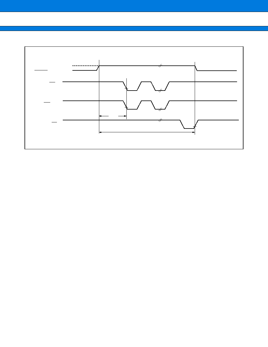
MB91360G Series
179
j : Temporary sector protect cancellation
Sector protect cancellation
t
VLHT
Write/erase command sequence
5 V
12 V
5 V
CS4X (WE)
BRQ (RY/BY)
BGRNTX (CE)
MD1
(RESET (V
ID
))
MB91360G Series
180
(10) AC Characteristics in Flash Memory Mode
The AC specifications for the external pins of the MB91360G series in the Flash Memory mode are shown below.
They apply to the case where the user performs read/write access in the Flash Memory mode. They are not
needed for access in the normal mode and for use of a flash memory writer.
The values are subject to change without prior notice.
a : Read access
AC Characteristics for Read Access
(Under recommended conditions)
Note : Sampled, not 100
%
tested.
Parameter
Symbol
Test
Condi-
tions
Value
Unit
Min
Typ
Max
Read cycle time
t
RC
120
ns
Address access time
t
ACC
CE
=
VIL
OE
=
VIL
120
ns
CE to data output
t
CE
OE
=
VIL
120
ns
OE to data output
t
OE
50
ns
CE to output floating
t
DF
30
ns
OE to output floating
t
DF
30
ns
Previous cycle data output hold time
t
OH
0
ns
INITX pin to return to read mode
t
Ready
20
µ
s
MB91360G Series
181
b : Write [write/erase command] access (WE control)
AC Characteristics for Write Access (WE Control)
(Under recommended conditions)
*1 : The internal preprogramming time before erasing is not included.
*2 : Applies only to sector protection
Note : Sampled, not 100
%
tested.
Parameter
Symbol
Value
Unit
Min
Typ
Max
Write cycle time
t
WC
120
ns
Address setup time
t
AS
0
ns
Address hold time
t
AH
50
ns
Data setup time
t
DS
50
ns
Data hold time
t
DH
0
ns
Output enable setup time
t
OES
0
ns
Output enable hold time
Read
t
OEH
0
ns
Toggle and data polling
10
ns
Read recovery time before write
t
GHWL
0
ns
CE setup time
t
CS
0
ns
CE hold time
t
CH
0
ns
Write pulse width
t
WP
50
ns
Write pulse width High level
t
WPH
20
ns
Write continuation time
t
WHWH1
8
µ
s
Sector erase continuation time*
1
t
WHWH2
1
15
s
V
CC
setup time
t
VCS
50
µ
s
Voltage transition time*
2
t
VLHL
4
µ
s
Write pulse width*
2
t
WPP
100
µ
s
OE setup time for validating WE*
2
t
OESP
4
µ
s
CE setup time for validating WE*
2
t
CSP
4
µ
s
INIT pulse width
t
RP
500
ns
RY/BY delay until write/erase is enabled
t
BUSY
50
ns
MB91360G Series
182
c : Write [write/erase command] access (CE control)
AC Characteristics for Write Access (CE Control)
(Under recommended conditions)
* : The internal preprogramming time before erasing is not included.
Note : Sampled, not 100
%
tested.
Parameter
Symbol
Value
Unit
Min
Typ
Max
Write cycle time
t
WC
120
ns
Address setup time
t
AS
0
ns
Address hold time
t
AH
50
ns
Data setup time
t
DS
50
ns
Data hold time
t
DH
0
ns
Output enable setup time
t
OES
0
ns
Output enable hold time
Read
t
OEH
0
ns
Toggle and data polling
10
ns
Read recovery time before write
t
GHWL
0
ns
WE setup time
t
WS
0
ns
WE hold time
t
WH
0
ns
CE pulse width
t
CP
50
ns
CE pulse width High level
t
CPH
20
ns
Write continuation time
t
WHWH1
16
µ
s
Sector erase continuation time*
t
WHWH2
1.5
30
s
V
CC
setup time
t
VCS
50
µ
s
INIT pulse width
t
RP
500
ns
RY/BY delay until write/erase is enabled
t
BUSY
50
ns
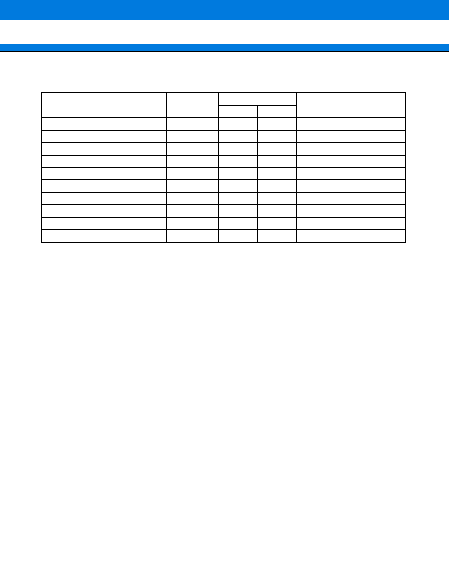
MB91360G Series
183
s
ELECTRICAL CHARACTERISTICS
1.
Absolute Maximum Ratings
*1 : Making full use of the allowed static DC correct into digital I/O will lead to lower values for V
IDIG
Min.
*2 :
∑
Applicable to pins : D0 to D31, A0 to A20, CS0X to CS6X, RDY, BGRNTX, BRQ, RDX, WR0X to WR3X, AS,
ALE, CLK, DREQ0, DACK0, DEOP0, INT0 to INT7, SGO, SGA, SDA, SCL, SOT0, SIN0,
SCK0, OCPA0 to OCPA3, TX0, TX1, RX0, RX1, SOT3 to SOT4, SIN3 to SIN4,
SCK3 to SCK4, LED0 to LED7 (MB91F362GA only) , IN0 to IN3 (MB91F362GA only) ,
OUT0 to OUT3 (MB91F362GA only) , OCPA4 to OCPA7 (MB91F362GA only) ,
SOT1 to SOT2 (MB91F362GA only) , SIH1 to SIH2 (MB91F362GA only) ,
SCK1 to SCK2 (MB91F362GA only) , PWM1P0 to PWM1P3 (MB91F362GA only) ,
PWM1M0 to PWM1M3 (MB91F362GA only) , PWM2P0 to PWM2P3 (MB91F362GA only) ,
PWM2M0 to PWM2M3 (MB91F362GA only)
∑
Use within recommended operating conditions.
∑
Use at DC voltage (current).
∑
The +B signal should always be applied with a limiting resistance placed between the +B signal and the
microcontroller.
∑
The value of the limiting resistance should be set so that when the +B signal is applied the input current to
the microcontroller pin does not exceed rated values, either instantaneously or for prolonged periods.
∑
Note that when the microcontroller drive current is low, such as in the power saving modes, the +B input
potential may pass through the protective diode and increase the potential at the VCC pin, and this may affect
other devices.
∑
Note that if a +B signal is input when the microcontroller current is off (not fixed at 0 V) , the power supply is
provided from the pins, so that incomplete operation may result.
∑
Note that if the +B input is applied during power-on, the power supply is provided from the pins and the resulting
supply voltage may not be sufficient to operate the power-on reset.
∑
Care must be taken not to leave the +B input pin open.
∑
Note that analog system input/output pins other than the A/D input pins (LCD drive pins, comparator input
pins, etc.) cannot accept +B signal input.
(Continued)
Parameter
Symbol
Rating
Unit
Condition
Min
Max
Digital supply voltage
V
DD
-V
SS
-
0.3
+
6.0
V
Stepper motor control supply voltage
HV
DD
-HV
SS
-
0.3
+
6.5
V
Storage temperature
Tstg
-
55
+
125
∞
C
Power consumption
P
TOT
2500
mW
T
A
=
+
25
∞
C
Digital input voltage
V
IDIG
-
0.3*
1
+
5.8
V
V
SS
=
0 V, V
DD
=
5 V
Analog input voltage
V
IA
-
0.3
+
5.8
V
V
SSA
=
0 V, V
DDA
=
5 V
Analog supply voltage
V
DDA
-V
SSA
-
0.3
+
5.8 V
V
SSA
=
0 V
Analog reference voltage
V
REFH
/
L
-
V
SSA
-
0.3
+
5.8
V
V
SSA
=
0 V
Static DC current into digital I/O
I
I/ODC
-
2.0
+
2.0
mA
*
2
Static total DC current into digital I/O
I
I/ODC
20
mA
*
2
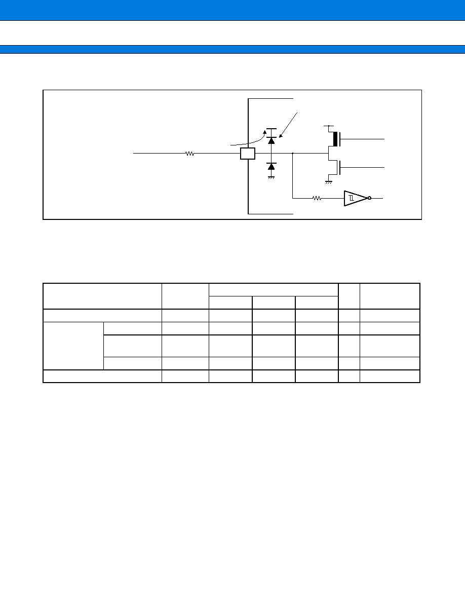
MB91360G Series
184
(Continued)
∑
Sample recommended circuits
WARNING: Semiconductor devices can be permanently damaged by application of stress (voltage, current,
temperature, etc.) in excess of absolute maximum ratings. Do not exceed these ratings.
2.
Recommended Operating Conditions
*: This is only valid if the integrated power-down reset circuit is switched-off, else a reset can be triggered at voltages
less or equal than 4.5 V (see "23. POWER DOWN RESET") .
WARNING: The recommended operating conditions are required in order to ensure the normal operation of the
semiconductor device. All of the device's electrical characteristics are warranted when the device is
operated within these ranges.
Always use semiconductor devices within their recommended operating condition ranges. Operation
outside these ranges may adversely affect reliability and could result in device failure.
No warranty is made with respect to uses, operating conditions, or combinations not represented on
the data sheet. Users considering application outside the listed conditions are advised to contact their
FUJITSU representatives beforehand.
Parameter
Symbol
Value
Unit
Condition
Min
Typ
Max
Operating temperature
T
A
-
40
+
85
∞
C
Supply voltage
(Internal voltage
regulator)
Digital supply
V
DD
- V
SS
4.25*
5
5.25
V
V
DDCORE
=
3.3 V
Stepper motor
control supply
HV
DD
- HV
SS
4.75
5
5.25
V
HV
SS
=
0 V
Analog supply
V
DDA
- V
SSA
4.9
5
5.1
V
V
SSA
=
0 V
RAM data retention voltage
V
DD
- V
SS
3.0
V
V
CC
P-ch
N-ch
R
∑
I/O equivalent circuit
Protective diode
Limiting
resistance
+
B input (0 V to 16 V)
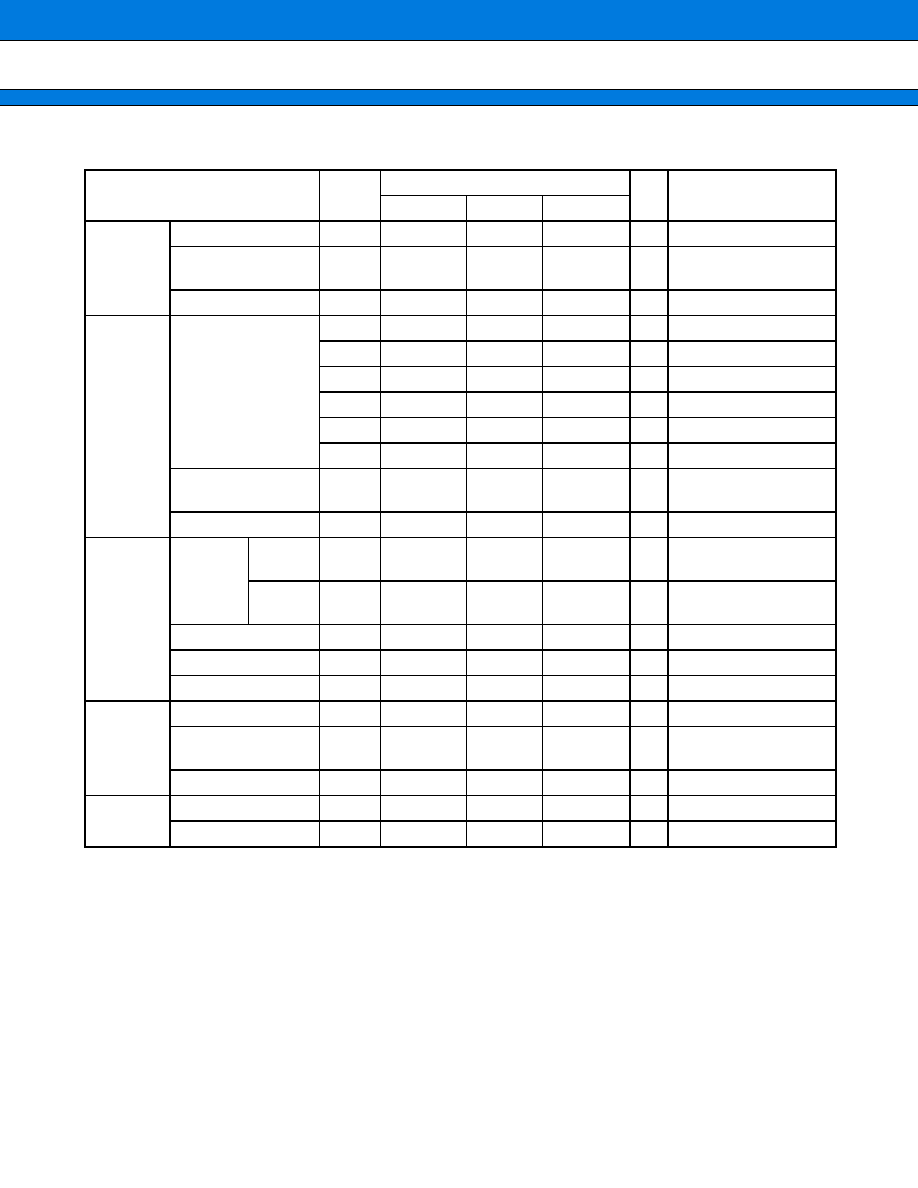
MB91360G Series
185
3.
DC Characteristics
*1 : See "4.
Run Mode Current
/
Power Consumption".
(Continued)
Parameter
Sym-
bol
Value
Unit
Condition
Min
Typ
Max
Current
consump-
tion
Run mode
I
srun
*1
mA
T
A
=
25
∞
C
RTC mode
I
sRTC
0.5
1.25
500
mA
µ
A
f
clk
=
4 MHz at T
A
=
25
∞
C
f
clk
=
32 kHz at T
A
=
25
∞
C
Stop mode
I
sstop
10
200
µ
A
f
clk
=
0 at
T
A
=
25
∞
C
Stepper
motor
control
H-port output voltage
V
OHH
HV
DD
-
500
HV
DD
-
125 mV
I
ol
=
±
30 mA, T
C
=
25
∞
C
V
OHL
HV
SS
+
125
HV
SS
+
500
mV
I
ol
=
±
30 mA, T
C
=
25
∞
C
V
OHH
HV
DD
-
500
HV
DD
-
125 mV
I
ol
=
±
27 mA, T
C
=
85
∞
C
V
OHL
HV
SS
+
125
HV
SS
+
500
mV
I
ol
=
±
27 mA, T
C
=
85
∞
C
V
OHH
HV
DD
-
500
HV
DD
-
125 mV
I
ol
=
±
30 mA, T
C
=
-
40
∞
C
V
OHL
HV
SS
+
125
HV
SS
+
500
mV
I
ol
=
±
30 mA, T
C
=
-
40
∞
C
SMC comparator
threshold voltage
V
THcomp
HV
DD
/
9
-
70
HV
DD
/
9
HV
DD
/
9
+
70
mV
Slew rate
40
ns
Cload
=
0 pF
Alarm
comparator
Threshold
voltage
Over-
voltage
V
TAH
4
/
5
V
DDA
-
5
%
4
/
5
V
DDA
4
/
5
V
DDA
+
5
%
V
(external 4 : 1 divider)
Under-
voltage
V
TAL
2
/
5
V
DDA
-
5
%
2
/
5
V
DDA
2
/
5
V
DDA
+
5
%
V
Switching hysteresis
V
TAHYS
12.5
25
50
mV
Alarm sense time
t
AS
10
µ
s
Input resistance
R
in
5
M
at V
TAH
, V
TAL
Power
down
Reset
Threshold voltage
V
TPOR
3.5
4.0
4.5
V
Switching hysteresis
V
TPO-
RHYS
20
50
80
mV
Reset sense time
t
RS
10
µ
s
Digital
outputs
Output "H" voltage
V
OH
V
DD
-
0.5
V
DD
V
I
load
=
4mA
Output "L" voltage
V
OL
V
SS
V
SS
+
0.4
V
I
load
=
-
4mA
MB91360G Series
186
(Continued)
*2 : valid for bidirectional tristate I/O PAD cell
Parameter
Symbol
Value
Unit
Condition
Min
Typ
Max
Digital
Inputs*
2
CMOS
(Type : Q, S,
Y, T)
High voltage
range
V
IH
0.65
◊
V
DD
V
DD
V
Low voltage
range
V
IL
V
SS
0.25
◊
V
DD
V
CMOS
Schmitt-
Trigger
(Types : E,
F, U)
High voltage
range
V
IH
0.8
◊
V
DD
V
DD
V
Low voltage
range
V
IL
V
SS
0.2
◊
V
DD
V
CMOS
Automotive
Schmitt-
Trigger
(Types : A,
B, K1, M1, J)
High voltage
range
V
IH
0.8
◊
V
DD
V
DD
V
Low voltage
range
V
IL
V
SS
0.5
◊
V
DD
V
hysteresis
voltage
0.5
V
CMOS 3/5 V
(Type : L, N,
O)
High voltage
range
V
IH
0.65
◊
V
DD
V
DD
V
Low voltage
range
V
IL
V
SS
0.25
◊
V
DD
V
CMOS 3 V
(Type : P, W)
High voltage
range
V
IH
0.65
◊
V
DD
V
DD
V
Low voltage
range
V
IL
V
SS
0.25
◊
V
DD
V
Input capaci-
tance
C
IN
16
pF
Input leakage
current
I
IL
-
1
+
1
µ
A
T
A
=
25
∞
C
Pull up
resistor
R
up1
R
up2
50
10
k
k
Types : E, U
Type : S
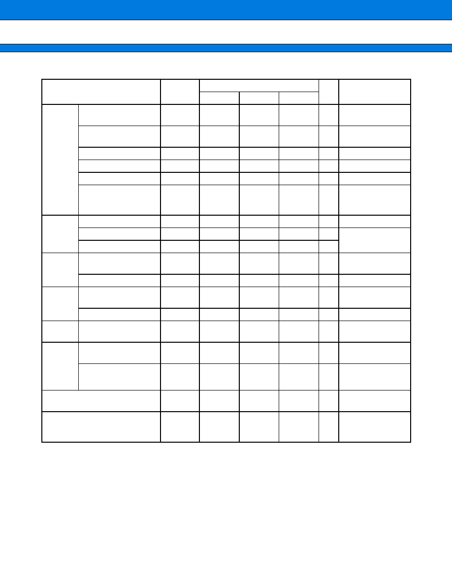
MB91360G Series
187
(Continued)
Parameter
Symbol
Value
Unit
Condition
Min
Typ
Max
ADC
inputs
Reference voltage input
V
REFH
V
REFL
V
REFL
+
3
V
SSA
V
DDA
V
REFH
-
3
V
V
Input voltage range
V
imax
V
imin
V
REFL
V
REFH
V
V
Input resistance
R
I
3.6
k
Input capacitance
C
I
30
pF
Input leakage current
I
IL
-
5
5
µ
A
Impedance of external
output driving the ADC
input
4.0
k
at sampling time of
1.6
µ
s
DAC
analog
outputs
Output voltage
V
out
V
SSA
V
DDA
V
Output impedance
R
out
2.9
k
external voltage
follower required
Output capacitance
C
out
20
pF
Sound
generator
Output voltage
V
outHIGH
V
outLOW
V
DD
-
0.5
V
SS
V
DD
V
SS
+
0.4
V
V
Output current
I
out
4
mA
PPG
Output voltage
V
outHIGH
V
outLOW
V
DD
-
0.5
V
SS
V
DD
V
SS
+
0.4
V
V
Output current
I
out
4
mA
LED
Output voltage
V
outHIGH
V
outLOW
V
DD
-
0.8
V
SS
+
0.8
V
V
I
outHIGH
=
14 mA
I
outLOW
=
24 mA
I
2
C Bus
Interface
(Open
Drain
Output)
Output voltage
V
outHIGH
V
outLOW
V
SS
V
DD
V
SS
+
0.4
V
V
open drain output
Output current
I
out
3
mA I
outLOW
=
3 mA
Lock-up time PLL1
(4 MHz
16 MHz to 64 MHz)
0.1
1
ms
ESD Protection
(Human body model MIL883-B
compliant)
V
surge
2
kV
R
discharge
=
1.5 k
C
discharge
=
100 pF
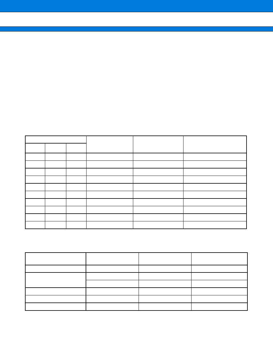
MB91360G Series
188
4.
Run Mode Current/Power Consumption
The power dissipation during normal operation is determined by the total power dissipation of the internal logic
P
C
, the dissipation from analog modules P
A
and the power dissipation P
IO
of the I/O buffers. Among the I/O buffers
the dissipation caused by the stepper motor drivers P
SMC
should be taken into special consideration.
So the overall power consumption P
D
will be calculated as a sum of Pc
+
P
A
+
P
SMC
+
P
IO .
(1) Logic Power Consumption
The following formula can be used to calculate the maximum core current consumption when the PLL is used
depending on the frequency settings for the internal clocks :
I
CC
=
3.45 [mA/MHz]
◊
CLKB [MHz]
+
2.52 [mA/MHz]
◊
CLKP[MHz]
+
0.72 [mA/MHz]
◊
CLKT [MHz]
+
35.5 mA.
If clock modulation is used the following value must be added to this result : 0.24 [mA/MHz]
◊
CLKB [MHz].
This results in the following values (higher clock settings are not allowed) :
In addition to this power consumption of the MCU core logic the following contributions to the overall power con-
sumption have to be considered :
(2) Analog Power Consumption
To calculate the analog power consumption P
A
, the current contributions of the active modules have to be multi-
plied by the maximum analog supply voltage of 5.1 V-or by the maximum digital supply voltage as in case of the
Power down reset.
Clock frequencies [MHz]
Maximum Core
Current
Consumption [mA]
Logic Power
Consumption
P
C
at 5.25 V [mW]
Remarks
CLKB
CLKP
CLKT
64
16
16
308
1.70
no clock modulation possible
48
24
24
290
1.52
48
16
16
264
1.40
32
32
32
257
1.35
32
16
16
205
1.08
24
24
24
202
1.06
24
12
12
163
0.86
16
16
16
146
0.77
2
2
2
40
0.21
no PLL, no clock modulation
0.125
0.125
0.125
30
0.16
no PLL, no clock modulation
Module
Typical Current
Consumption
Maximum Current
Consumption
Remarks
DAC
1 mA / channel
current at AVCC
ADC
3 mA
7 mA
current at AVCC
1.6 mA
2.6 mA
current at AVRH
Power down reset
0.26 mA
0.5 mA
current at Vdd
Alarm Comparator
0.31 mA
0.5 mA
current at AVCC
Zero point detection
0.13 mA
0.25 mA
current at AVCC
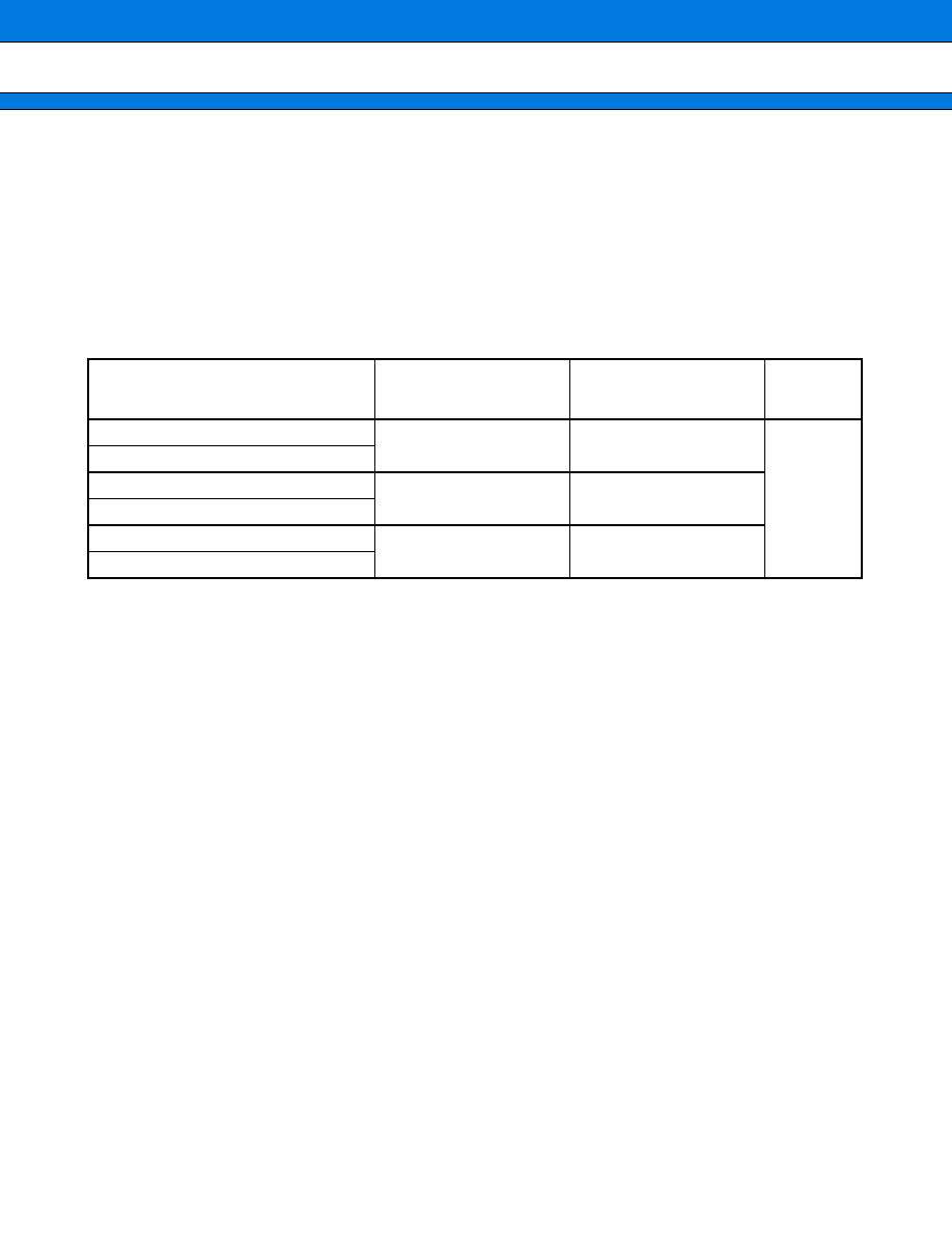
MB91360G Series
189
(3) I/O and SMC Power Consumption
SMC drivers :
The average current consumption per SMC channel is 38.2 mA, for four channels this results in 152.8 mA.
At 2
◊
0.5 V this results in 153 mW power consumption P
SMC
for four channels of stepper motor drivers.
Other I/O Buffers :
The power dissipation (P
IO
) (at 5.25 V) of the I/O buffers is represented as the sum of the dynamic power
dissipation (P
AC
) and the static power consumption (P
DC
) .
P
IO
=
P
AC
◊
1.1
+
P
DC
The following table lists values for the calculation of P
AC5V
and P
AC3V
:
P
AC
=
P
IB
◊
In
◊
f
◊
operating rate
+
P
OB
◊
On
◊
f
◊
operating rate
P
DC
is the caused by off chip loads which are drawing static currents.
P
DC
=
VO
◊
IO
◊
DC
N
Buffer Type
Power Consumption
P
IB
/P
OB
@ 5V
to calculate P
AC5V
Power Consumption
P
IB
/P
OB
@ 3.3V
to calculate P
AC3V
Unit
Normal Input
12.4
12.4
µ
W/MHz
(C
L
in pF)
Bidirectional Input
4 mA Bidirectional Output
194
+
25 C
L
85.5
+
11 C
L
4 mA Output
8 mA Bidirectional Output
353
+
25 C
L
154
+
11 C
L
8 mA Output
P
IB
:
Power Consumption of Input Buffers and Bidirectional Inputs
P
OB
:
Power Consumption of Output Buffers and Bidirectional Outputs
In :
Total number of input buffers and bidirectional buffer inputs
On :
Total number of output buffers and bidirectional buffer outputs
f :
System frequency
Operating rate : 1.0 if all buffers are switched simultaneously at system frequency
VO :
Output voltage drop - usually 0.4 V
IO :
Output current - usually 4 mA
DC
N
:
Number of output buffers and bidirectional buffers driving off chip loads causing static currents.
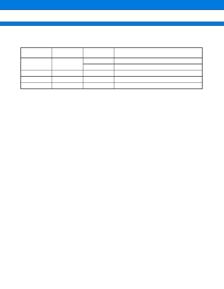
MB91360G Series
190
5.
Clock Settings
Note : F362GA : If the maximum frequency of 64 MHz is set for CLKB and an odd division factor for CLKT (3, 5, 7,
9, 11, 13, 15) has been selected, then the option to create an asymmetrical CLKT must be used (set bit 14
of the F362MD register to "1") .
Clock domain
Clock name
Max frequency
setting
Remark
Core
CLKB
64 MHz
under normal operating conditions
32 MHz
for supply voltage between 4.25 and 3.5 V
Resource bus
CLKP
32 MHz
Ext. Bus
CLKT
32 MHz
Clock for CAN
CANCLK
32 MHz
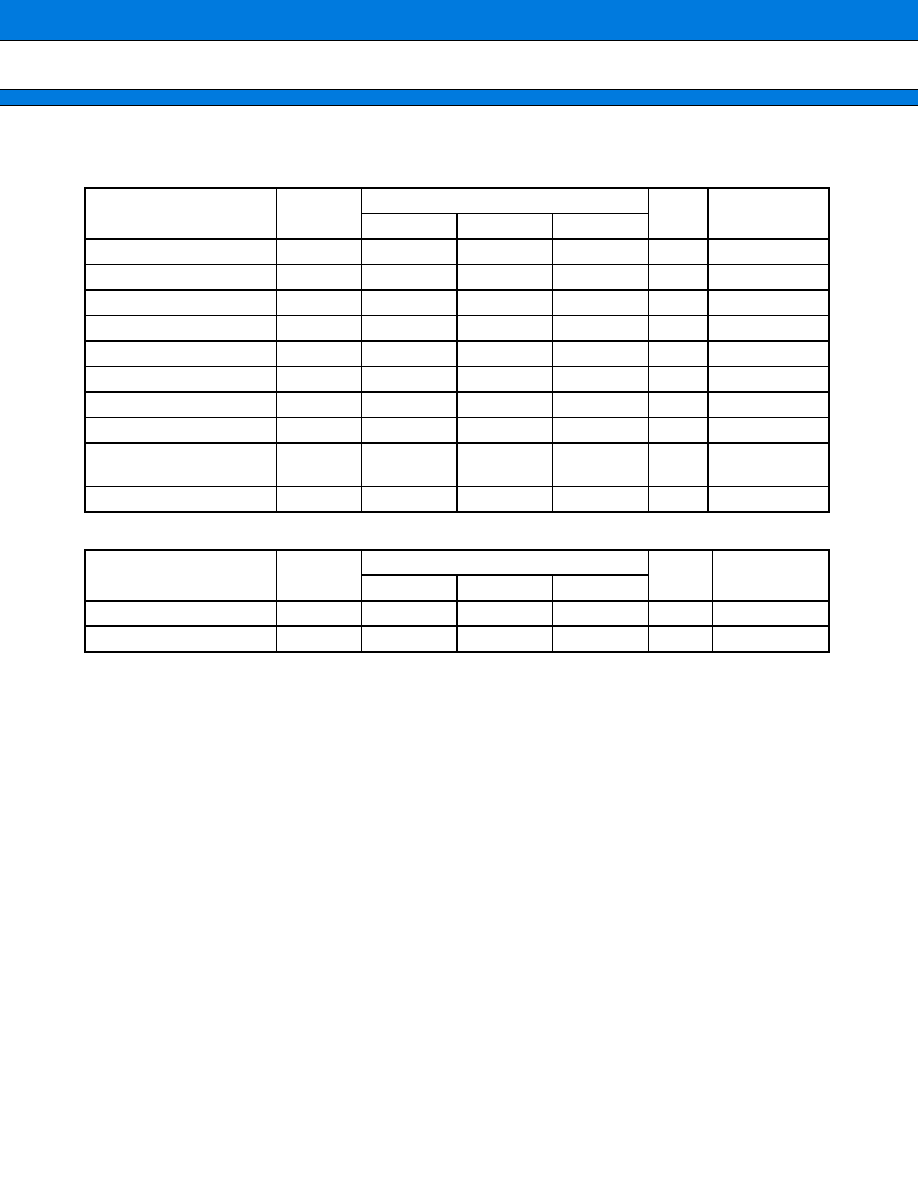
MB91360G Series
191
6.
Converter Characteristics
∑ A/D Converter
∑ D/A Converter
Parameter
Symbol
Value
Unit
Remark
Min
Typ
Max
Resolution
10
Bit
Conversion error
±
5.0
LSB
overall error
Non-linearity
±
2.5
LSB
Differential Non-linearity
±
1.9
LSB
Zero Reading voltage
V
0T
AVRL
-
3.5
AVRL
+
0.5
AVRL
+
4.5
LSB
Full scale reading voltage
V
FST
AVRH
-
5.5
AVRH
-
1.5
AVRH
+
2.5
LSB
Input current
IA@V
DDA
3.0
7.0
mA
Reference voltage current
IR
1.6
2.6
mA
Conversion time
178 cycles
CLKP
1 ms
Ripple of supply voltage
±
5.0
mV
Parameter
Symbol
Value
Unit
Remark
Min
Typ
Max
Resolution
10
Bit
Differential linearity error
-
0.9
+
0.9
LSB
MB91360G Series
192
7.
A/D Converter Glossary
∑ Resolution
The smallest change in analog voltage detected by A/D converter.
∑ Linearity error
A deviation of actual conversion characteristic from a line connecting the zero-traction point (between "00 0000
0000"
"00 0000 0001") to the full-scale transition point (between "11 1111 1110"
"11 1111 1111") .
∑ Differential linearity error
A deviation of a step voltage for changing the LSB of output code from ideal input voltage.
∑ Total error
A difference between actual value and theoretical value. The overall error includes zero-transition error, full-
scale transition error and linearity error.
(Continued)
3FF
3FE
3FD
004
003
002
001
AVRL
AVRH
1.5 LSB'
0.5 LSB'
{1 LSB'
◊
(N
-
1)
+
0.5 LSB'}
Digital output
Analog input
Actual conversion
characteristic
Actual conversion
Ideal characteristic
V
NT
(measured value)
Total error of digital output N
=
V
NT
-
{1 LSB'
◊
(N
-
1)
+
0.5 LSB'}
1 LSB'
[LSB]
V
OT
' (Ideal value)
=
AVRL
+
0.5 LSB' [V]
V
FST
' (Ideal value)
=
AVRH
-
1.5 LSB' [V]
V
NT
: A voltage for causing transition of digital output from (N
-
1) to N
Total error
MB91360G Series
193
(Continued)
3FF
3FE
3FD
004
003
002
001
AVRL
AVRH
{1 LSB
◊
(N
-
1)
+
V
OT
}
V
NT
(measured value)
V
OT
(measured value)
Digital output
Actual conversion characteristic
Ideal characteristic
Analog input
Actual conversion
characteristic
V
FST
(measured value)
N
-
1
AVRL
AVRH
N
-
2
N
N
+
1
Actual conversion
characteristic
Actual conversion
characteristic
Ideal characteristic
V
NT
(measured value)
V
(N
+
1)T
(measured value)
Digital output
Analog input
Linearity error of digital output N
=
V
NT
-
{1 LSB
◊
(N
-
1)
+
V
OT
}
1 LSB
[LSB]
Differential linearity error of digital output N
=
V (
N
+
1
)
T
-
V
NT
1 LSB
-
1 [LSB]
1 LSB
=
V
FST
-
V
OT
1022
[V]
1 LSB' (ideal value)
=
AVRH
-
AVRL
1023
[V]
V
OT
: A voltage for causing transition of digital output from (000)
H
to (001)
H
V
FST
: A voltage for causing transition of digital output from (3FE)
H
to (3FF)
H
V
NT
: A voltage for causing transition of digital output from (N
-
1)
H
to N
Linearity error
Differential linearity error

MB91360G Series
194
8.
Notes on Using A/D Converter
Output impedance of external circuit of analog input under following conditions;
Output impedance of external circuit
<
4 k
.
If output impedance of external circuit is too high, analog voltage sampling time may be too short for accurate
sampling.
∑ Error
As the absolute value of AVRH decreases, relative error increases.
R
O
R
ON
: 3.6 K
Analog input pin
Comparator
C
0
C
0
: 30 pF
∑ Analog input Equivalent Circuit
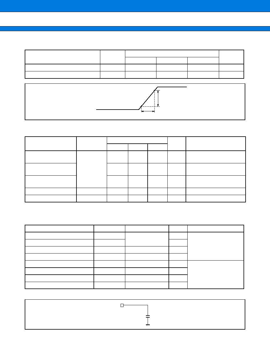
MB91360G Series
195
9.
The Time for Power Supply
10. Flash Memory
∑
∑
∑
∑
Erase and programming performance
* : T
A
=
+
85
∞
C, V
DD
=
5.0 V
11. AC Characteristics
∑
∑
∑
∑
Measurement conditions
Load conditions
Parameter
Symbol
Value
Unit
Min
Typ
Max
Power supply raising slope
V/
t
0.05
V/
µ
s
Power supply raising slope
t
R
80
µ
s
Parameter
Condition
Value
Unit
Remarks
Min
Typ
Max
Sector erase time
T
A
=
+
25
∞
C,
V
DD
=
5.0 V
1
15*
s
Excludes 00H programming
prior erasure
Chip erase time
14
s
Excludes 00H programming
prior erasure
Half word (16-bit)
programming time
16
3,600*
µ
s
Excludes system-level
overhead
Erase/Program cycle
10,000
cycle
Data retention time
100 K
h
Parameter
Symbol
Value
Unit
Conditions
"H" level input voltage
V
IH
according to I/O spec
V
V
DD
=
4.25 to 5.25 V,
T
A
=
-
40 to
+
85
∞
C
"L" level input voltage
V
IL
V
"H" level output voltage
V
OH
0.5
◊
V
DD
V
"L" level output voltage
V
OL
0.5
◊
V
DD
V
"H" level input voltage
V
IH
3.0
V
V
DD
=
3.0 to 3.6 V,
T
A
=
-
40 to
+
85
∞
C
"L" level input voltage
V
IL
0
V
"H" level output voltage
V
OH
0.5
◊
V
DD
V
"L" level output voltage
V
OL
0.5
◊
V
DD
V
V
DD
4.2 V
0.2 V
t
V
C
=
50 pF
Output pin
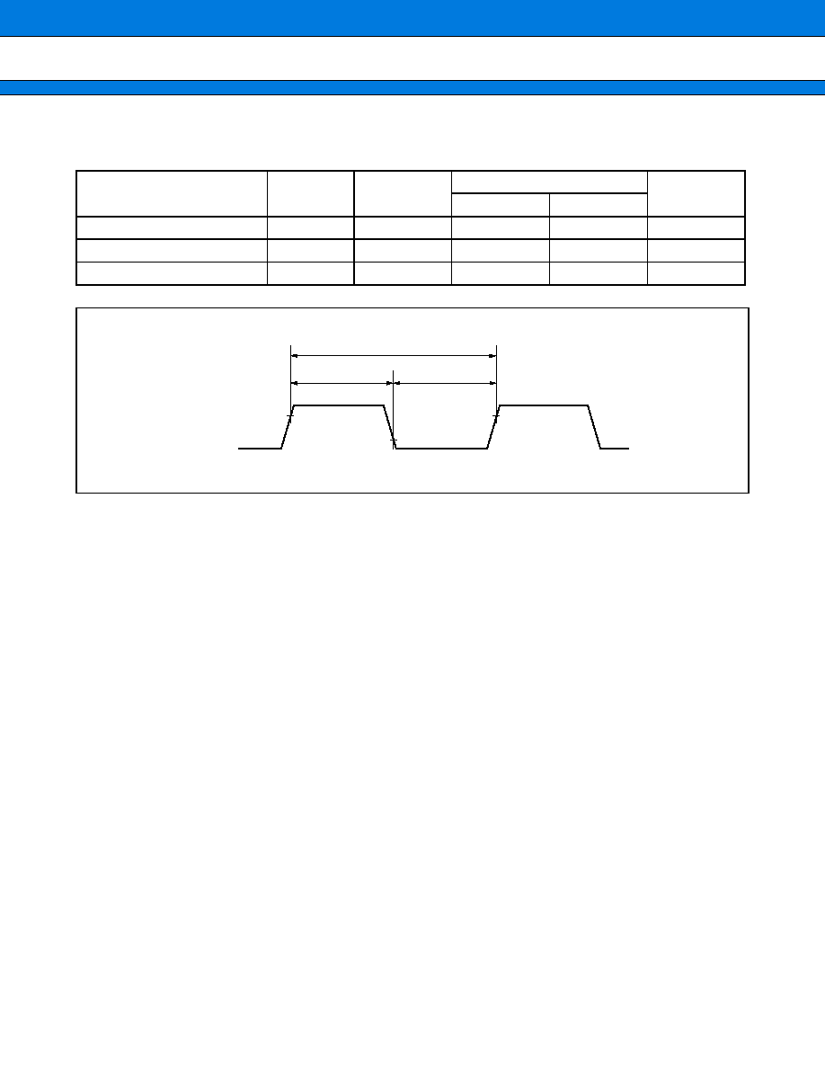
MB91360G Series
196
∑
∑
∑
∑
External bus clock
(V
DD
=
4.25 V to 5.25 V, T
A
=
-
40
∞
C to
+
85
∞
C)
Note : This is only valid for operation without clock modulator
The values for t
CHCL
and t
CLCH
are heavily dependent on the load connected to the CLK pin. The following diagrams
show this dependency for the worst case situation. The first diagram shows the situation for even division ratios
between CLKB and CLKT, the second diagram shows this for odd division ratios between CLKB and CLKT
(ASYMCLKT bit is not set) .
It has to note that when the combination of CLK frequency and load at CLK pin is such that rise or fall times are
longer than t
CYC
/
2 the duty ratio can get worse.
Signal
Symbol
Pin name
Value
Unit
Min
Max
CLK cycle
t
CYC
CLK
t
CPT
ns
CLK rise
CLK fall
t
CHCL
CLK
t
CYC
/
2
-
10
t
CYC
/
2
+
10
ns
CLK fall
CLK rise
t
CLCH
CLK
t
CYC
/
2
-
10
t
CYC
/
2
+
10
ns
CLK
t
CYC
V
OH
V
OH
V
OL
t
CHCL
t
CLCH
MB91360G Series
197
Even CLKB/CLKT division ratios :
Odd CLKB/CLKT division ratios :
14,0
12,0
10,0
8,0
6,0
4,0
2,0
0,0
0
20
40
60
pF
ns
80
100
120
5 V
3.3 V
deviation of t
CHCL
from t
CYC
/
2 versus load
14,0
12,0
10,0
8,0
6,0
4,0
2,0
0,0
0
20
40
60
pF
ns
80
100
120
5 V
3.3 V
deviation of t
CHCL
from t
CYC
/
2 versus load
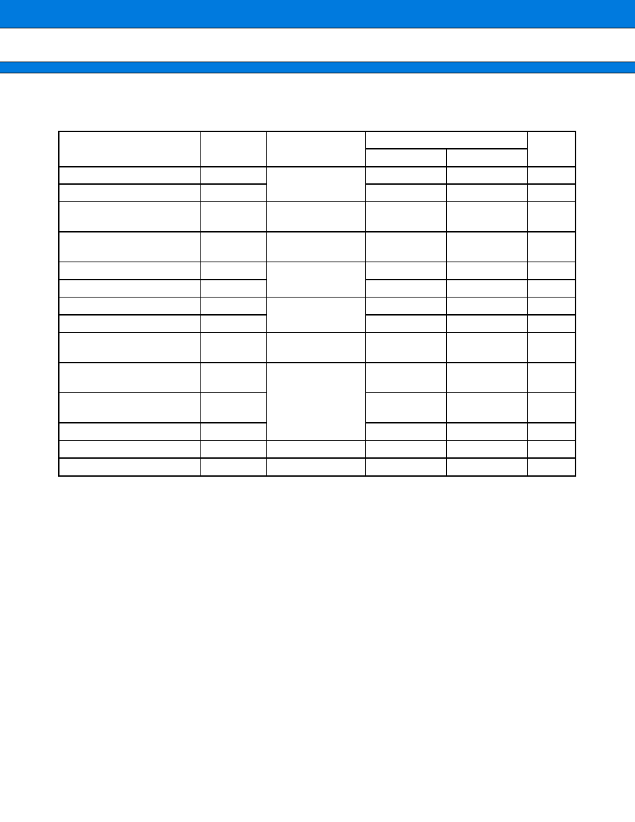
MB91360G Series
198
∑
∑
∑
∑
External bus interface
(V
DD
=
4.25 V to 5.25 V, T
A
=
-
40
∞
C to
+
85
∞
C)
Signal
Symbol
Pin name
Value
Unit
Min
Max
CS6X to CS0X delay time
t
CHCSL
CLK
CS6X to CS0X
15
ns
CS6X to CS0X delay time
t
CHCSH
15
ns
Address delay time
t
CHAV
CLK
A20 to A0
20
ns
Data delay time
t
CHDV
CLK
D31 to D0
16
ns
RDX delay time
t
CLRL
CLK
RDX
15
ns
RDX delay time
t
CLRH
15
ns
WR3X to WR0X delay time
t
CLWL
CLK
WR3X to WR0X
15
ns
WR3X to WR0X delay time
t
CLWH
15
ns
Effective address
Effect data input time
t
AVDV
A20 to A0
D31 to D0
3
/
2
◊
t
CYC
-
30
ns
RDX (fall)
Effect data input time
t
RLDV
RDX
D31 to D0
t
CYC
-
20
ns
Data set up
RDX (rise) time
t
DSRH
25
ns
RDX (rise)
Data hold time
t
RHDX
0
ns
AS delay time
t
CHASL
AS
15
ns
AS delay time
t
CHASH
AS
15
ns
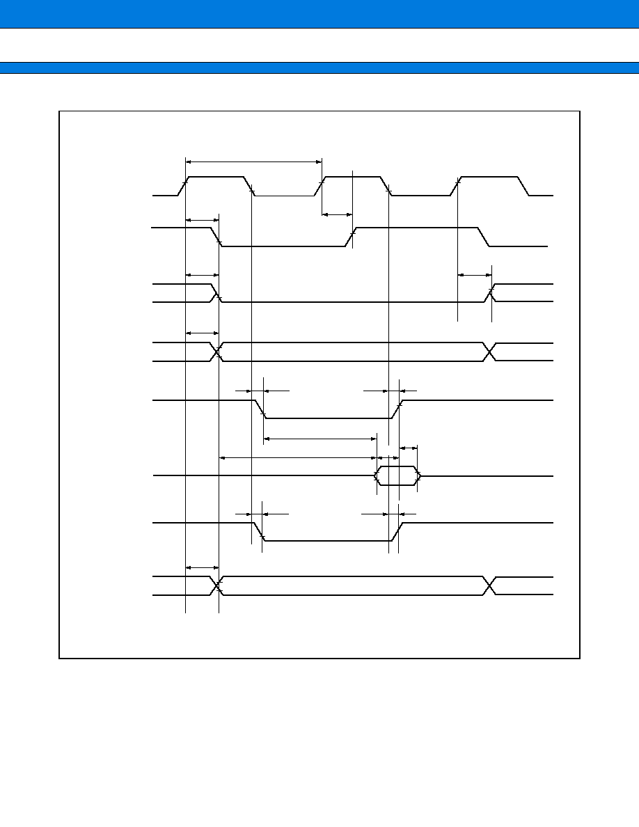
MB91360G Series
199
V
OH
V
OH
CLK
AS
V
OL
V
OL
V
OH
V
OH
V
OL
V
OL
V
OH
V
OL
t
CLRL
V
OL
t
CLWL
V
OL
t
CHDV
V
OL
V
OH
t
CLRH
V
OH
V
OH
V
OL
V
OH
V
OL
t
RHDX
V
OH
t
CHCSH
V
OH
CS0X - CS6X
A23 - A00
RDX
D31 - D00
WR3X - WR0X
D31 - D00
t
CYC
t
CHCSL
t
CHASL
t
RLDV
t
AVDV
t
CHASH
t
CLWH
t
CHAV
t
DSRH
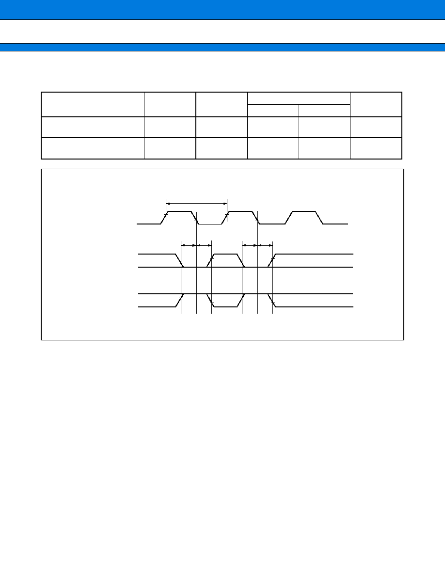
MB91360G Series
200
∑
∑
∑
∑
RDY
(V
DD
=
4.25 V to 5.25 V, T
A
=
-
40
∞
C to
+
85
∞
C)
Signal
Symbol
Pin name
Value
Unit
Min
Max
RDY setup
t
RDYS
CLK
RDY
16
ns
RDY hold
t
RDYH
CLK
RDY
0
ns
CLK
V
OH
V
OH
V
OL
V
OL
V
IL
V
IH
V
IH
V
IL
t
RDYH
t
RDYH
RDY
case 1
RDY
case 2
t
CYC
t
RDYS
t
RDYS
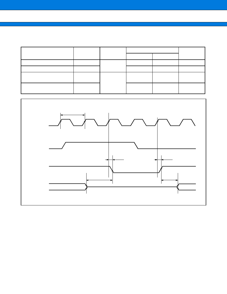
MB91360G Series
201
∑
∑
∑
∑
BGRNTX
(V
DD
=
4.25 V to 5.25 V, T
A
=
-
40
∞
C to
+
85
∞
C)
Signal
Symbol
Pin name
Value
Unit
Min
Max
BGRNTX
t
CHBGL
CLK
BGRNTX
10
ns
BGRNTX
t
CHBGH
10
ns
Bus access enabled
BGRNTX falling
t
XHAL
BGRNTX
tcyc
- 15
tcyc
+ 15
ns
Bus access disabled
BGRNTX rising
t
HAHV
tcyc
- 15
tcyc
+ 15
ns
CLK
V
OH
t
CHBGL
V
OH
V
OH
V
OH
t
CHBGH
BRQ
BGRNTX
Other
Ports
t
CYC
t
HAHV
t
XHAL
High-Z
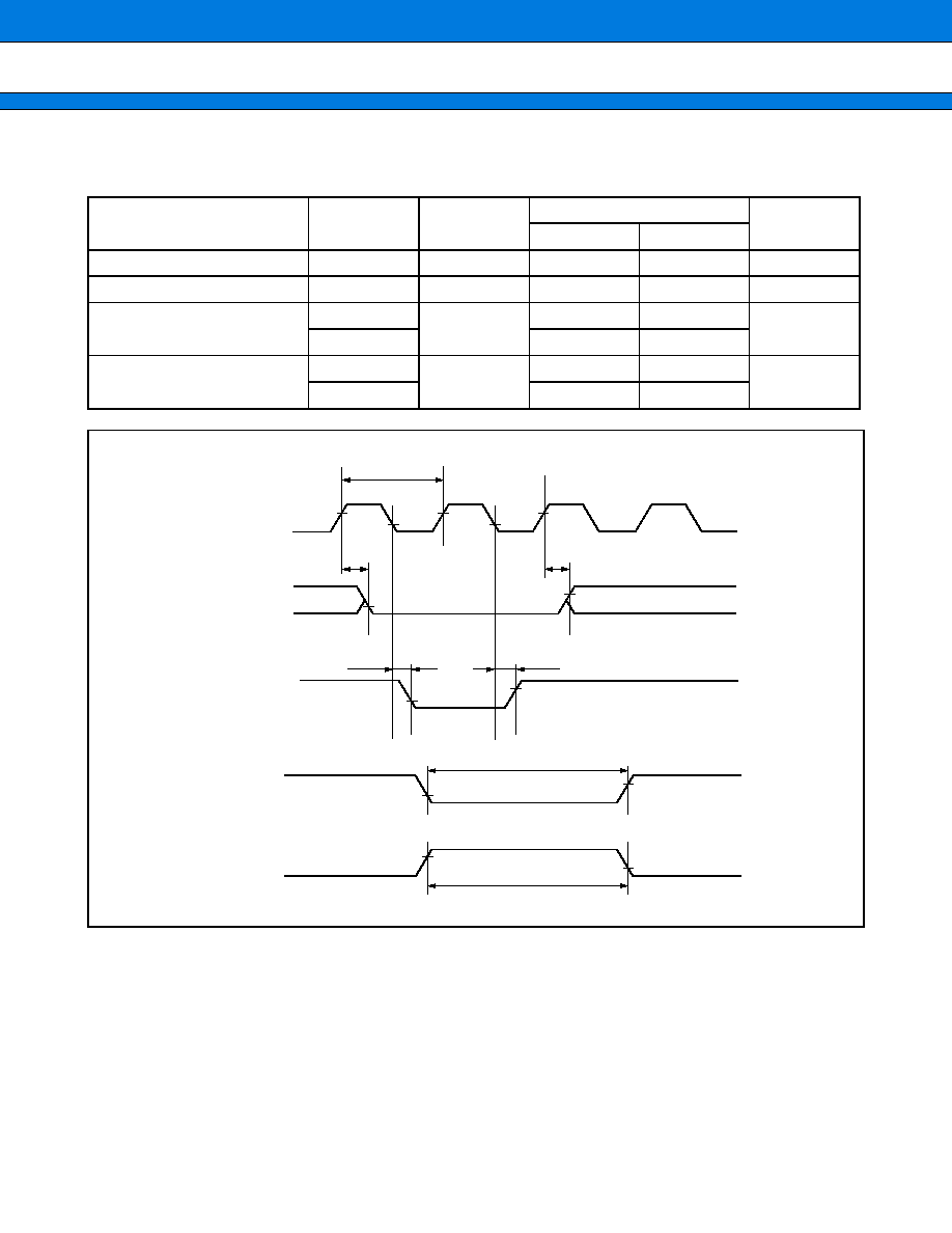
MB91360G Series
202
∑
∑
∑
∑
DMA
(V
DD
=
4.25 V to 5.25 V, T
A
=
-
40
∞
C to
+
85
∞
C)
* : DSTP and DEOP share a pin. The pin is possible to change DSTP and DEOP functions using a port function
register.
Signal
Symbol
Pin name
Value
Unit
Min
Max
DREQ
t
DRWH
DREQ0
5t
CYC
ns
DSTP
t
DSWH
DSTP0*
5t
CYC
ns
DACK
t
CLDL
CLK
DACK0
20
ns
t
CLDH
20
DEOP
t
CLEL
CLK
DEOP0
20
ns
t
CLEH
20
CLK
DSTP0
DREQ0
DACK0
DEOP0
t
CYC
t
DSWH
t
DRWH
t
CLDL
t
CLDH
t
CLEL
t
CLEH
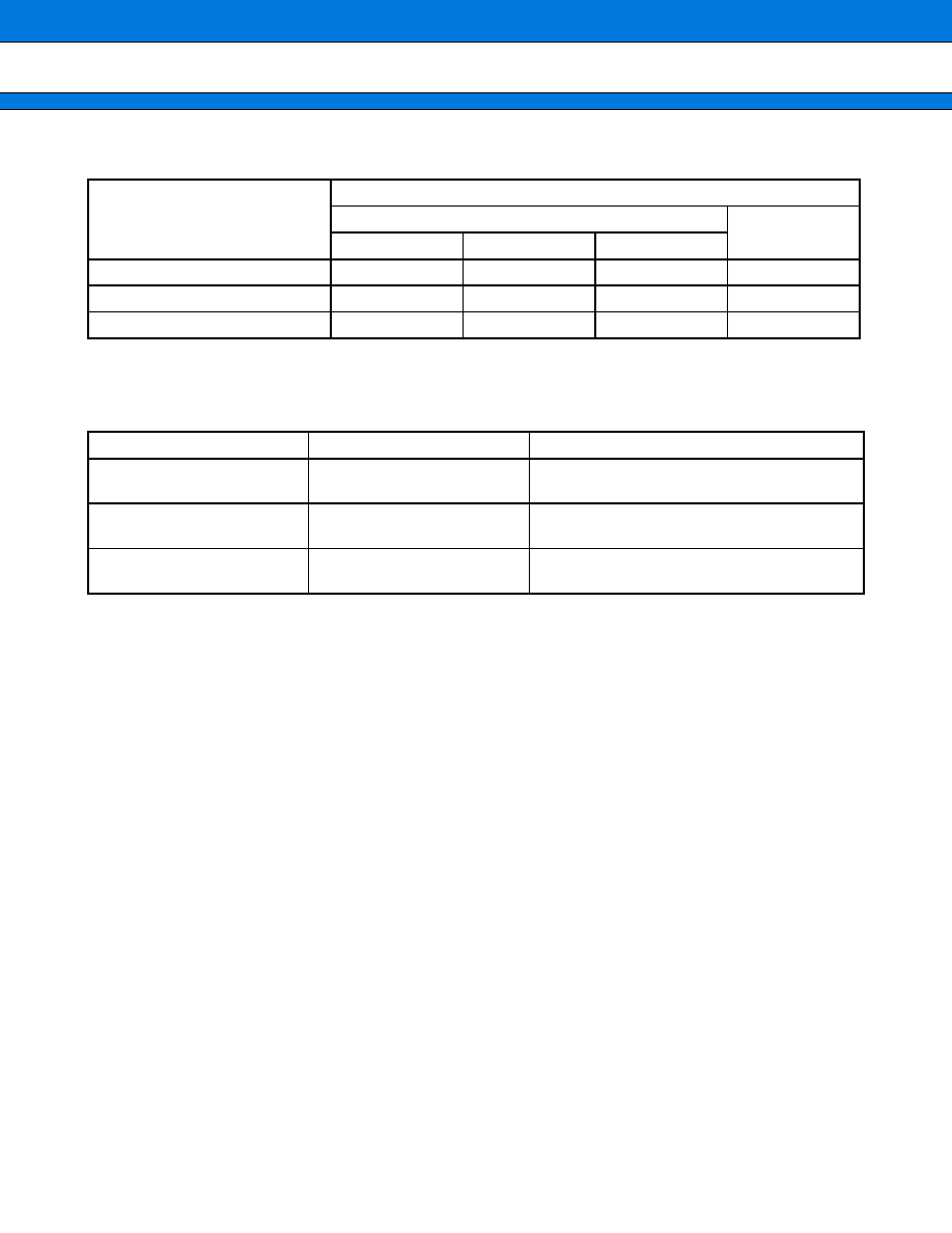
MB91360G Series
203
s
PACKAGE THERMAL RESISTANCE INFORMATION
s
ORDERING INFORMATION
Package
Thermal Resistance [
∞
∞
∞
∞
C/W]
Theta-ja
Theta-jc
0 m/s
1 m/s
3 m/s
FPT-208P-M04
16
13
11
2.5
PGA-401C-A02
16
8.5
5.5
FPT-160P-M15
16
13
11
2.5
Part number
Package
Remarks
MB91FV360GACR
401-pin Ceramic PGA
(PGA-401C-A02)
MB91F362GAPFVS
208-pin Plastic QFP
(FPT-208P-M04)
MB91F369GAPQS1
160-pin Plastic QFP
(FPT-160P-M15)
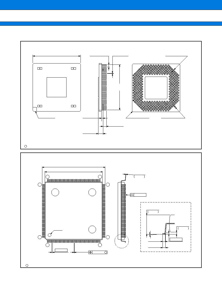
MB91360G Series
204
s
PACKAGE DIMENSIONS
(Continued)
401-pin ceramic PGA
(PGA-401C-A02)
208-pin plastic QFP
(FPT-208P-M04)
Note : Pins width and pins thickness include plating thickness.
48.26 ± 0.55
(1.900 ± .022)
SQ
INDEX AREA
1994 FUJITSU LIMITED R401002SC-2-2
2.54 (.100) TYP
0.40 ± 0.10
(.016 ± .004)
DIA
45.72 (1.800)
REF
1.20 ± 0.25
(.047 ± .010)
5.27 (.207)
MAX
3.40 ± 0.40
(.134 ± .016)
1.00 (.039) DIA TYP
(4 PLCS)
EXTRA INDEX PIN
1.02 (.040) C TYP
(4 PLCS)
C
Dimensions in mm (inches)
C
2000 FUJITSU LIMITED F208020S-c-2-3
.148
≠.012
+.008
≠0.30
+0.20
3.75
Details of "A" part
0.50±0.20
(.020±.008)
0.60±0.15
(.024±.006)
0.25(.010)
(Stand off)
0.40
+0.10
≠0.15
+.004
≠.006
.016
0∞~8∞
1
LEAD No.
52
53
104
105
156
157
208
"A"
0.08(.003)
0.50(.020)
0.22±0.05
(.009±.002)
0.08(.003)
M
28.00±0.10(1.102±.004)SQ
30.60±0.20(1.205±.008)SQ
.007
≠.003
+.001
≠0.08
+0.03
0.17
INDEX
(Mounting height)
Dimensions in mm (inches)
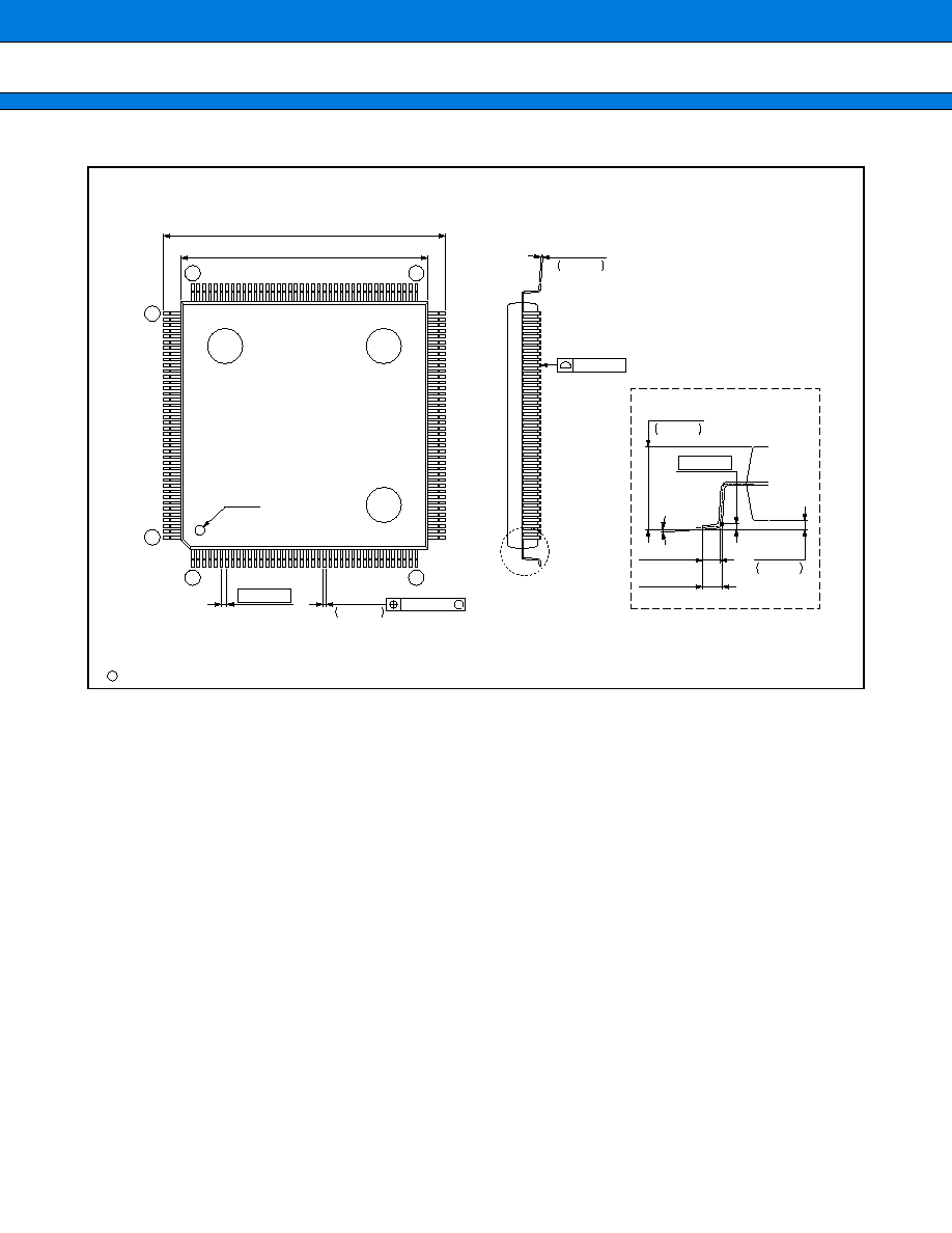
MB91360G Series
205
(Continued)
160-pin plastic QFP
(FPT-160P-M15)
Note : Pins width and pins thickness include plating thickness.
C
2001 FUJITSU LIMITED F160037S-c-2-2
M
0.13(.005)
28.00±0.20(1.102±.008)SQ
32.00±0.40(1.260±.016)SQ
0.65(.026)
0.10(.004)
"A"
(Mounting height)
Details of "A" part
INDEX
1
40
121
160
120
81
≠0.07
+0.08
0.32
.013
+.0031
≠.0028
≠0.03
+0.05
0.17
.007
+.002
≠.001
0~8∞
≠0.20
+0.35
3.75
.148
+.014
≠.008
0.25(.010)
(Stand off)
≠0.15
+0.10
0.40
.016
+.004
≠.006
0.80±0.20
(.031±.008)
0.88±0.15
(.035±.006)
Dimensions in mm (inches)

MB91360G Series
FUJITSU LIMITED
All Rights Reserved.
The contents of this document are subject to change without notice.
Customers are advised to consult with FUJITSU sales
representatives before ordering.
The information and circuit diagrams in this document are
presented as examples of semiconductor device applications, and
are not intended to be incorporated in devices for actual use. Also,
FUJITSU is unable to assume responsibility for infringement of
any patent rights or other rights of third parties arising from the use
of this information or circuit diagrams.
The products described in this document are designed, developed
and manufactured as contemplated for general use, including
without limitation, ordinary industrial use, general office use,
personal use, and household use, but are not designed, developed
and manufactured as contemplated (1) for use accompanying fatal
risks or dangers that, unless extremely high safety is secured, could
have a serious effect to the public, and could lead directly to death,
personal injury, severe physical damage or other loss (i.e., nuclear
reaction control in nuclear facility, aircraft flight control, air traffic
control, mass transport control, medical life support system, missile
launch control in weapon system), or (2) for use requiring
extremely high reliability (i.e., submersible repeater and artificial
satellite).
Please note that Fujitsu will not be liable against you and/or any
third party for any claims or damages arising in connection with
above-mentioned uses of the products.
Any semiconductor devices have an inherent chance of failure. You
must protect against injury, damage or loss from such failures by
incorporating safety design measures into your facility and
equipment such as redundancy, fire protection, and prevention of
over-current levels and other abnormal operating conditions.
If any products described in this document represent goods or
technologies subject to certain restrictions on export under the
Foreign Exchange and Foreign Trade Law of Japan, the prior
authorization by Japanese government will be required for export
of those products from Japan.
F0201
©
FUJITSU LIMITED Printed in Japan