FUJITSU SEMICONDUCTOR
Data Sheet (Advance Information)
Advance Information
MB90495 Series Data Sheet (Advance Information)
1 / 40
FME EMDC June 19, 2000
16-bit Proprietary Microcontroller
CMOS
F
2
MC-16LX MB90495 Series
MB90497/F497
1. OUTLINE
The MB90495-series with FULL-CAN interface and FLASH ROM is especially designed for automotive and industrial applications.
Its main feature is the on-chip CAN Interface, which conforms to V2.0 Part A and Part B, while supporting a very flexible message
buffer scheme, including 8 message buffers, and so offering more functions than a normal full CAN approach.
With the new 0.5 mm CMOS technology, Fujitsu now also offers on-chip FLASH-ROM program memory. An internal voltage
booster removes the necessity for a second programming voltage. An on-chip voltage regulator provides 3V to the internal MCU
core. This creates a major advantage in terms of EMI and power consumption.
The internal PLL clock frequency multiplier provides an internal 62.5 nsec instruction cycle time from an external 4 MHz clock. A
32kHz Subsystem clock has been included for power saving modes and real time measurement.
There are 2 on-chip UART's, which also provide synchronous communication modes. Furthermore the MCU features an 8 chan-
nel ADC, 8 channel External interrupt controller, two 16 bit PPG channels, 4 channel Input Capture Unit and a 16-bit free running
I/O-timer.

MB90495 Series
MB90495 Series Data Sheet (Advance Information)
2 / 40
FMG EMDC June 19, 2000
2. FEATURES
�
16-bit core CPU; 4MHz external clock (16 MHz internal, 62.5 ns instruction cycle time)
�
32kHz Subsystem Clock
�
0.5 mm CMOS Technology
�
Internal voltage regulator supports 3V MCU core, offering low EMI and low power consump-
tion figures
�
64 KB FLASH ROM; supports automatic programming, 10.000 erase cycles, 10 year data
retention time and no second programming voltage required
�
2 KB static RAM
�
FULL-CAN interface; conforming to Version 2.0 Part A and Part B, flexible message buffering
(mailbox and FIFO buffering can be mixed)
�
2 UART's; both offering synchronous communication modes.
�
Powerful interrupt functions (8 programmable priority levels; 8 external interrupts)
�
I/O Timer
�
A/D Converter: 8 channel analogue inputs (Resolution 10 bits or 8 bits)
�
ICU (Input capture) 16bit * 4ch
�
PPG (Programmable Pulse Generator) 16bit * 2ch; Can be configured as 8bit * 4ch
�
Optimised instruction set for controller applications
(bit, byte, word and long-word data types; 23 different addressing modes; barrel shift; variety
of pointers)
�
4-byte instruction execution queue
�
Signed multiply (16bit*16bit) and divide (32bit/16bit) instructions available
�
Program Patch Function
�
Fast Interrupt processing
�
16-bit reload timer: 2 channels
�
Low Power Consumption - Several different Lo-Power modes: (Sleep, Stop, Watch,...)
�
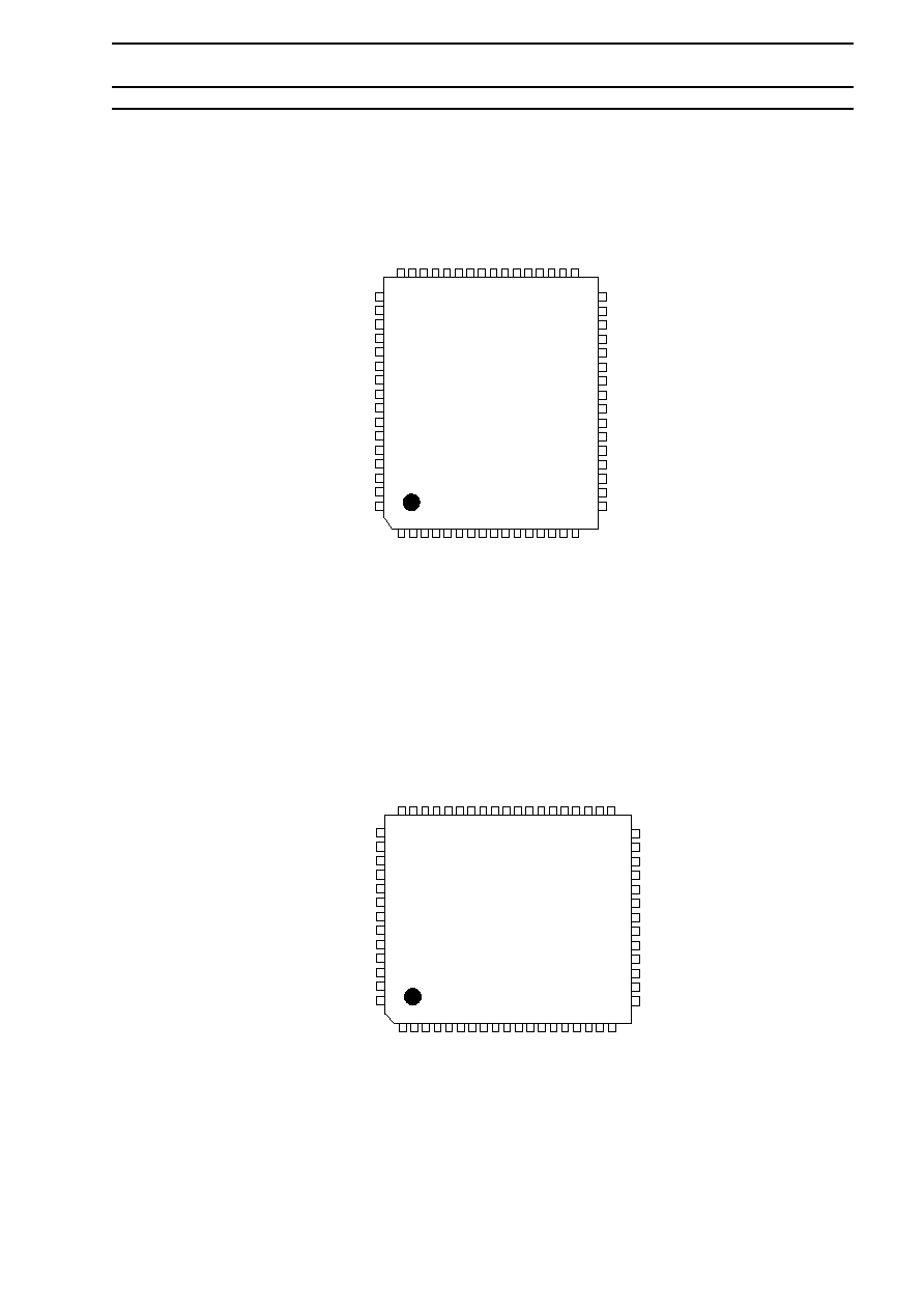
Package:
QFP-64; 12mm x 12mm body, 0.65mm pin pitch
�
QFP-64; 20mm x 18mm body, 1.0mm pin pitch

MB90495 Series
MB90495 Series Data Sheet (Advance Information)
3 / 40
FME EMDC June 19, 2000
3. PRODUCT LINEUP
The following table provides an overview of the MB90495 Series
Features
MB90F497
MB90497
CPU
F2MC-16LX CPU
System clock
On-chip PLL clock multiplier (x1, x2, x3, x4, 1/2 when PLL stop)
Minimum instruction execution time: 62.5 ns (4 MHz osc. PLL x4)
ROM
Boot-block
Flash memory 64 Kbytes
Mask ROM 64 Kbytes
RAM
2 Kbytes
2 Kbytes
Technology
0.5 mm CMOS with on-chip voltage regulator
for internal power supply + Flash memory On-
chip charge pump for programming voltage
0.5 mm CMOS with on-chip voltage regulator for
internal power supply
Operating
voltage range
5 V +/- 10%
Temperature
range
- 40 to 85
�
C
Package
QFP64