 | –≠–ª–µ–∫—Ç—Ä–æ–Ω–Ω—ã–π –∫–æ–º–ø–æ–Ω–µ–Ω—Ç: F5CM | –°–∫–∞—á–∞—Ç—å:  PDF PDF  ZIP ZIP |
DS04-23119-4E
FUJITSU SEMICONDUCTOR
DATA SHEET
ASSP
Mobile Communication Systems
Piezoelectric SAW BPF
(700 MHz to 1000 MHz)
F5CM Series (B2)
s
s
s
s
DESCRIPTION
The F5CM series of SAW filters have balanced in/unbalanced out or unbalanced in/balanced out of I/O ports.
Therefore these filters are suitable for the design using balanced type of IC. By using these filters, any transforming
devises, such as balun is not required.
The F5CM series filters apply to the frequency range 700 MHz to 1000 MHz. High performance has been realized
with high reliability and small size by using original materials and original design.
The F5CM series filters are suitable for RF interstage filter in mobile communication systems and standard parts
are available for GSM and AMPS/TDMA/CDMA standards.
s
s
s
s
FEATURES
∑ Balanced/unbalanced I/O ports
∑ Ultra compact and light package (3.0 mm
◊
3.0 mm package)
∑ Any external matching network is not required
∑ Excellent stop-band attenuation
∑ Small pass-band ripple
∑ Surface mount package (SMT)
s
s
s
s
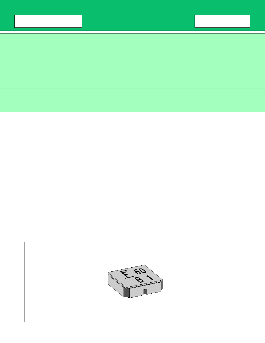
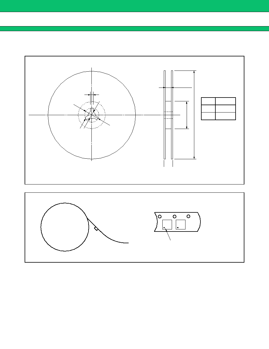
PACKAGE
F5CM Series (B2)
2
s
s
s
s
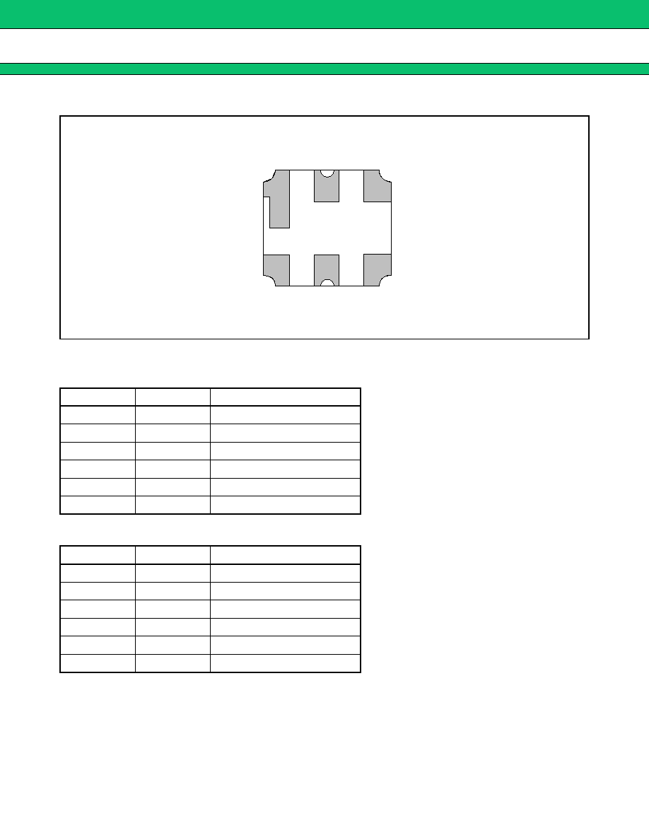
PIN ASSIGNMENT
s
s
s
s
PIN DESCRIPTIONS
∑ BALANCED IN/UNBALANCED OUT type (Tx filter)
∑ UNBALANCED IN/BALANCED OUT type (Rx filter)
Pin no.
Pin name
Description
1
GND
Ground Pin
2
OUT
Unbalanced output Pin
3
GND
Ground Pin
4
IN
Balanced Input Pin
5
GND
Ground Pin
6
IN
Balanced Input Pin
Pin no.
Pin name
Description
1
GND
Ground Pin
2
IN
Unbalanced Input Pin
3
GND
Ground Pin
4
OUT
Balanced Output Pin
5
GND
Ground Pin
6
OUT
Balanced Output Pin
(BOTTOM VIEW)
6
5
4
1
2
3
F5CM Series (B2)
3
s
s
s
s
ABSOLUTE MAXIMUM RATINGS
WARNING: Piezoelectric devices can be permanently damaged by application of stress (voltage, current,
temperature, etc.) in excess of absolute maximum ratings. Do not exceed these ratings.
s
s
s
s
RECOMMENDED OPERATING CONDITION
WARNING: The recommended operating conditions are required in order to ensure the normal operation of the
piezoelectric device. All of the device's electrical characteristics are warranted when the device is
operated within this range.
Always use piezoelectric devices within their recommended operating conditionranges. Operation
outside these ranges may adversely affect reliability and could result in device failure.
No warranty is made with respect to uses, operating conditions, or combinations not represented on
the data sheet. Users considering application outside the listed conditions are advised to contact their
FUJITSU representatives beforehand.
s
s
s
s
STANDARD DEVICES
Parameter
Symbol
Rating
Unit
Min.
Max.
Operating temperature
Ta
-
30
+
85
∞
C
Storage temperature
Tstg
-
40
+
100
∞
C
Input power
P
IN
+
15
dBm
Input DC Voltage
-
5
+
5
V
Parameter
Symbol
Value
Unit
Min.
Max.
Operating temperature
Ta
-
30
+
85
∞
C
System
Frequency
(MHz)
Band
width
(MHz)
Input type/
Impedance
Output type/
Impedance
Part number
Part
symbol
GSM
Tx
902.5
25
Balance
50
Unbalance
50
FAR-F5CM-902M50-B263
63
Rx
947.5
25
Unbalance
50
Balance
50
FAR-F5CM-947M50-B260
60
Balance
150
FAR-F5CM-947M50-B262
62
EGSM
Rx
942.5
25
Unbalance
50
Balance
50
FAR-F5CM-942M50-B270
70
AMPS/
TDMA/
CDMA
Tx
836.5
25
Balance
50
Unbalance
50
FAR-F5CM-836M50-B268
68
Rx
881.5
25
Unbalance
50
Balance
50
FAR-F5CM-881M50-B266
66
F5CM Series (B2)
4
s
s
s
s
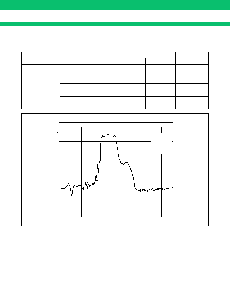
ELECTRICAL CHARACTERISTICS AND TYPICAL FREQUENCY RESPONSE
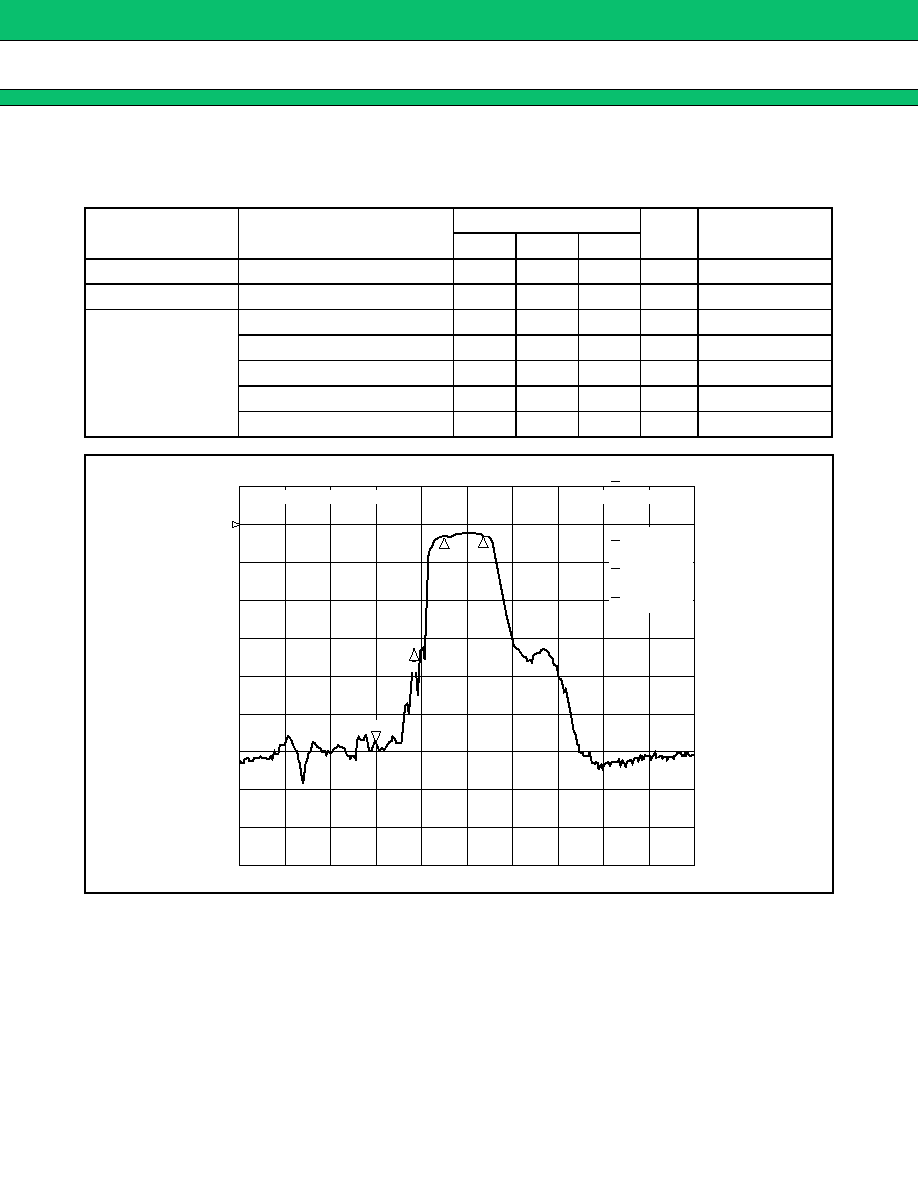
1.
GSM (Tx) 50 ohms Balanced IN/50 ohms Unbalanced OUT
Part number : FAR-F5CM-902M50-B263
(Ta
=
-
30
∞
C to
+
85
∞
C)
Parameter
Conditions
Value
Unit
Remarks
Min.
Typ.
Max.
Insertion loss
890 MHz to 915 MHz
3.2
3.5
dB
Pass-band ripple
890 MHz to 915 MHz
1.2
1.5
dB
Absolute
stop-band
attenuation
DC to 845 MHz
45
58
dB
845 MHz to 870 MHz
25
50
dB
935 MHz to 980 MHz
25
30
dB
980 MHz to 2000 MHz
40
58
dB
2000 MHz to 3000 MHz
30
37
dB
1
2
3
4
log
MAG
10 dB/
REF
0 dB
1
: -
3.192 dB
0.890 000 000 GHz
2
: -
2.773 dB
0.9150 GHz
3
: -
29.56 dB
0.9350 GHz
4
: -
34.57 dB
0.9500 GHz
FAR-F5CM-902M50-B263
CENTER
900 MHz
SPAN
300 MHz
F5CM Series (B2)
5
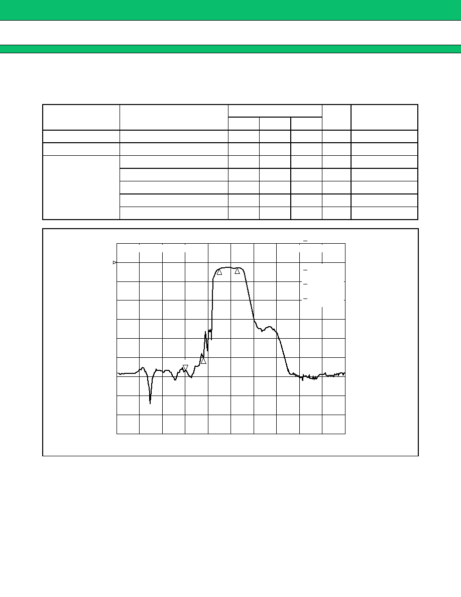
2.
GSM (Rx) 50 ohms Unbalanced IN/50 ohms Balanced OUT
Part number : FAR-F5CM-947M50-B260
(Ta
=
-
30
∞
C to
+
85
∞
C)
Parameter
Conditions
Value
Unit
Remarks
Min.
Typ.
Max.
Insertion loss
935 MHz to 960 MHz
3.0
3.3
dB
Pass-band ripple
935 MHz to 960 MHz
0.9
1.2
dB
Absolute
stop-band
attenuation
DC to 890 MHz
45
56
dB
890 MHz to 915 MHz
25
31
dB
980 MHz to 1025 MHz
25
30
dB
1025 MHz to 2000 MHz
40
50
dB
2000 MHz to 3000 MHz
35
45
dB
3
4
log
MAG
10 dB/
REF
0 dB
0.890 000 000 GHz
FAR-F5CM-947M50-B260
CENTER
950 MHz
SPAN
300 MHz
1
: -
58.133 dB
2
: -
32.723 dB
0.9150 GHz
3
: -
2.999 dB
0.9350 GHz
4
: -
2.808 dB
0.9600 GHz
2
1
F5CM Series (B2)
6
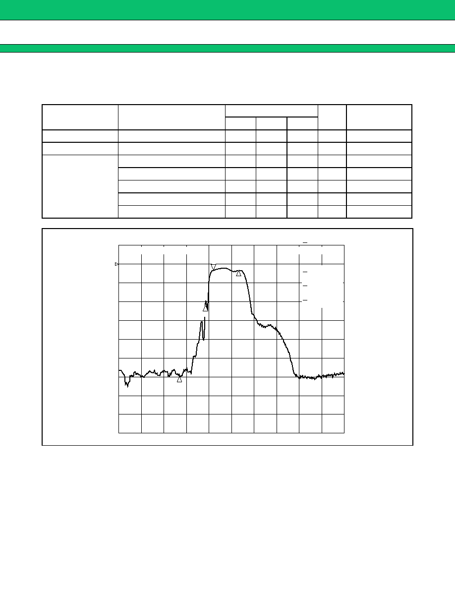
3.
GSM (Rx) 50 ohms Unbalanced IN/150 ohms Balanced OUT
Part number : FAR-F5CM-947M50-B262
(Ta
=
-
30
∞
C to
+
85
∞
C)
Parameter
Conditions
Value
Unit
Remarks
Min.
Typ.
Max.
Insertion loss
935 MHz to 960 MHz
3.3
3.8
dB
Pass-band ripple
935 MHz to 960 MHz
0.8
1.3
dB
Absolute
stop-band
attenuation
DC to 890 MHz
45
55
dB
890 MHz to 915 MHz
25
48
dB
980 MHz to 1025 MHz
23
29
dB
1025 MHz to 2000 MHz
40
50
dB
2000 MHz to 3000 MHz
35
39
dB
3
4
log
MAG
10 dB/
REF
0 dB
0.890 000 000 GHz
FAR-F5CM-947M50-B262
CENTER
950 MHz
SPAN
300 MHz
1
: -
55.741 dB
2
: -
50.182 dB
0.9150 GHz
3
: -
3.077 dB
0.9350 GHz
4
: -
3.028 dB
0.9600 GHz
1
2
F5CM Series (B2)
7
4.
EGSM (Rx) 50 ohms Unbalanced IN/50 ohms Balanced OUT
Part number : FAR-F5CM-942M50-B270
(Ta
=
-
30
∞
C to
+
85
∞
C)
Parameter
Conditions
Value
Unit
Remarks
Min.
Typ.
Max.
Insertion loss
925 MHz to 960 MHz
3.8
4.5
dB
Pass-band ripple
925 MHz to 960 MHz
1.8
2.5
dB
Absolute
stop-band
attenuation
DC to 880 MHz
50
55
dB
880 MHz to 915 MHz
15
22
dB
980 MHz to 1025 MHz
23
27
dB
1025 MHz to 2000 MHz
40
44
dB
2000 MHz to 3000 MHz
25
39
dB
3
4
log
MAG
10 dB/
REF
0 dB
925. 000 000 MHz
FAR-F5CM-942M50-B270
CENTER
950 MHz
SPAN
300 MHz
1
: -
3.5649 dB
2
: -
2.9961 dB
960 MHz
3
: -
59.498 dB
880 MHz
4
: -
20.549 dB
915 MHz
1
2
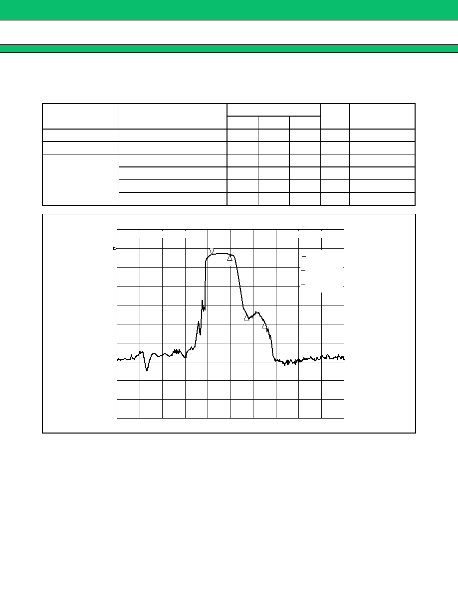
F5CM Series (B2)
8
5.
AMPS/TDMA/CDMA (Tx) 50 ohms Balanced IN/50 ohms Unbalanced OUT
Part number : FAR-F5CM-836M50-B268
(Ta
=
-
30
∞
C to
+
85
∞
C)
Parameter
Conditions
Value
Unit
Remarks
Min.
Typ.
Max.
Insertion loss
824 MHz to 849 MHz
2.8
3.5
dB
Pass-band ripple
824 MHz to 849 MHz
0.9
1.6
dB
Absolute
stop-band
attenuation
DC to 800 MHz
45
52
dB
869 MHz to 920 MHz
25
33
dB
920 MHz to 2000 MHz
35
46
dB
2000 MHz to 3000 MHz
25
33
dB
3
log
MAG
10 dB/
REF
0 dB
0.824 000 000 GHz
FAR-F5CM-836M50-B268
CENTER
850 MHz
SPAN
300 MHz
1
: -
2.566 dB
2
: -
2.763 dB
0.8490 GHz
3
: -
33.493 dB
0.8690 GHz
4
: -
38.685 dB
0.8940 GHz
2
4
1
F5CM Series (B2)
9
6.
AMPS/TDMA/CDMA (Rx) 50 ohms Unbalanced IN/50 ohms Balanced OUT
Part number : FAR-F5CM-881M50-B266
(Ta
=
-
30
∞
C to
+
85
∞
C)
Parameter
Conditions
Value
Unit
Remarks
Min.
Typ.
Max.
Insertion loss
869 MHz to 894 MHz
2.8
3.5
dB
Pass-band ripple
869 MHz to 894 MHz
0.8
1.5
dB
Absolute
stop-band
attenuation
DC to 800 MHz
45
55
dB
800 MHz to 849 MHz
30
47
dB
940 MHz to 1000 MHz
30
38
dB
1000 MHz to 2000 MHz
35
47
dB
2000 MHz to 3000 MHz
25
32
dB
3
4
log
MAG
10 dB/
REF
0 dB
0.824 000 000 GHz
FAR-F5CM-881M50-B266
CENTER
900 MHz
SPAN
300 MHz
1
: -
57.172 dB
2
: -
48.219 dB
0.8490 GHz
3
: -
2.836 dB
0.8690 GHz
4
: -
2.825 dB
0.8940 GHz
2
1
F5CM Series (B2)
10
s
s
s
s
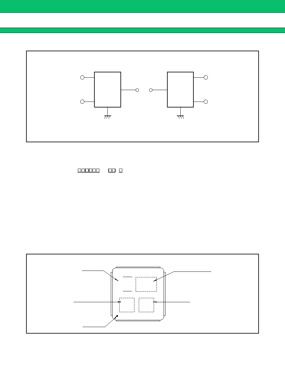
MEASURMENT CIRCUIT
s
s
s
s
PART NUMBER DESIGNATION
s
s
s
s
MARKING
2
1 3
6
5
4
I n p u t
5 0
O u t p u t
5 0
O u t p u t
5 0
/
1 5 0
1 3
5
2
6
4
I n p u t
5 0
BALANCED IN/UNBALANCED OUT type
(Tx filter)
UNBLANCED IN/BALANCED OUT type
(Rx filter)
Note : Attached frequency response plots are obtained by simulation using above S21, S31, S32, S11,
S22, S33 of each characteristics. Electrical specifications are also decided based on these results.
1 to 6 : Pin Number
[Designation example]
(1) Frequency : Center frequency is specified in six alphanumeric.
Enter M (for MHz) at the decimal point.
Refer to below example.
[Example]902.5 MHz
902M50
(2) Part symbol : Specified characters from 60 to 79.
(3) Packing :
Y : 1 k pcs/reel
(Reeled tape) X : 5 k pcs/reel
FAR
-
F5CM
-
-
B2
-
(1)
(2) (3)
F
B 1
60
PART SYMBOL
LOGO
DATE CODE
LOT No.
INDEX
F5CM Series (B2)
11
s
s
s
s
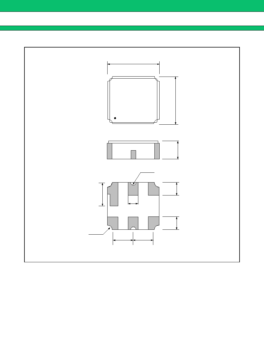
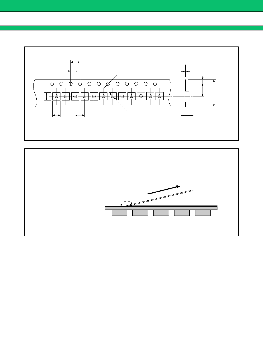
PACKAGE DIMENSION
3.0
3.0
1.2 Max.
0.75
0.75
1.2
0.6
1.5
1.2
2
-
R 0.2
6
5
4
1
2
3
4
-
R 0.3
Dimensions in mm.
F5CM Series (B2)
12
s
s
s
s
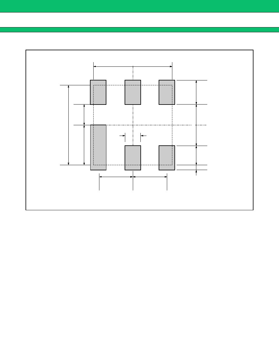
RECOMMENDED LAND PATTERN
3.0
0.70
1.20
3.0
0.75
1.5
0.2
0.75
0.95
1.20
1.5
Dimensions in mm.
F5CM Series (B2)
13
s
s
s
s
PACKING
1.
Reel Dimensions
2.
Packing Style
1.5 Min.
12.8 Min.
20.2 Min.
R 0.58
9.5
±
0.5
80
250
13.8 Max.
Type
Volume
Y
1 k pcs
X
5 k pcs
Dimensions in mm.
1 P I N
Pulling side
Reel side
Pulling side
F5CM Series (B2)
14
3.
Tape Dimensions
4.
Peel Strength of Top Cover Tapes
4.0
±
0.1
2.0
±
0.05
3.5
±
0.05
3.3
±
0.1
1.5
±
0.1
0.0
1.0 Min.
0.3
±
0.05
8.0
±
0.2
4.0
±
0.1
3.3
±
0.1
1.75
±
0.1
1.3
±
0.1
Dimensions in mm.
Embossment carrier type tape
Direction of pulling
Speed 300 mm/min
Peel off by the force of 0.1 N to 1.0 N under the condition at the right.
(Conforms to EIA.)
165
∞
to 180
∞
F5CM Series (B2)
15
s
s
s
s
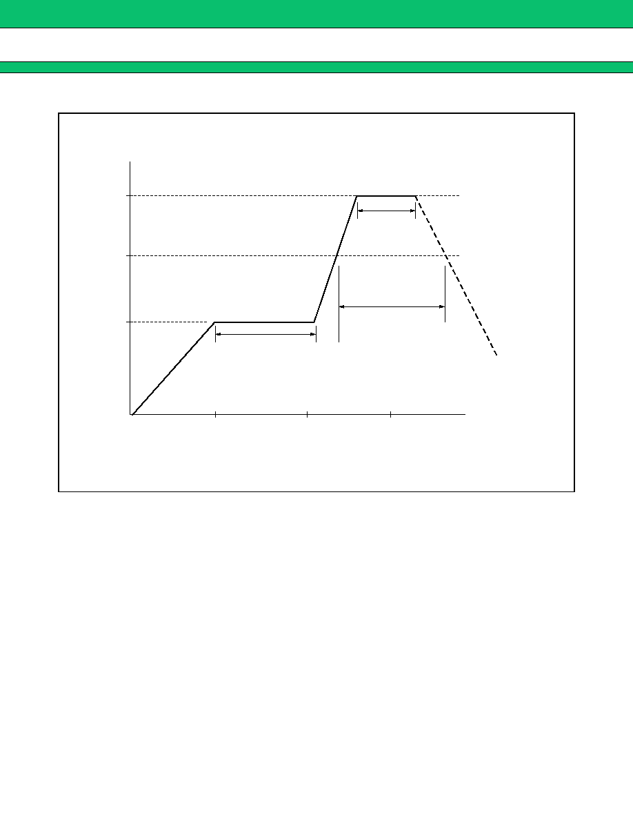
RECOMMENDED REFLOW PROFILE
s
s
s
s
NOTE
Mass-produced product order is accepted by a unit of 1000.
240
210
150
Pre-Heating
10 s
60 s
60 s
90 s
Time (s)
Air cooling
Heating rate
1
∞
C/s to 4
∞
C/s
Temperatur
e (
∞
C)

F5CM Series (B2)
FUJITSU LIMITED
All Rights Reserved.
The contents of this document are subject to change without notice.
Customers are advised to consult with FUJITSU sales
representatives before ordering.
The information and circuit diagrams in this document are
presented as examples of semiconductor device applications, and
are not intended to be incorporated in devices for actual use. Also,
FUJITSU is unable to assume responsibility for infringement of
any patent rights or other rights of third parties arising from the use
of this information or circuit diagrams.
The products described in this document are designed, developed
and manufactured as contemplated for general use, including
without limitation, ordinary industrial use, general office use,
personal use, and household use, but are not designed, developed
and manufactured as contemplated (1) for use accompanying fatal
risks or dangers that, unless extremely high safety is secured, could
have a serious effect to the public, and could lead directly to death,
personal injury, severe physical damage or other loss (i.e., nuclear
reaction control in nuclear facility, aircraft flight control, air traffic
control, mass transport control, medical life support system, missile
launch control in weapon system), or (2) for use requiring
extremely high reliability (i.e., submersible repeater and artificial
satellite).
Please note that Fujitsu will not be liable against you and/or any
third party for any claims or damages arising in connection with
above-mentioned uses of the products.
Any semiconductor devices have an inherent chance of failure. You
must protect against injury, damage or loss from such failures by
incorporating safety design measures into your facility and
equipment such as redundancy, fire protection, and prevention of
over-current levels and other abnormal operating conditions.
If any products described in this document represent goods or
technologies subject to certain restrictions on export under the
Foreign Exchange and Foreign Trade Law of Japan, the prior
authorization by Japanese government will be required for export
of those products from Japan.
F0107
©
FUJITSU LIMITED Printed in Japan