
FUJITSU SEMICONDUCTOR
DATA SHEET
DS07-20101-7E
Resonator
Piezoelectric Resonator
FAR Family (C1, C3, C4 series)
s
DESCRIPTION
Fujitsu resonators (C1, C3, C4 series) feature originally developed single crystals with a high electromechanical
coupling coefficient (LiTaO
3
: lithium tantalate, LiNbO
3
: lithium niobate), the result is compact packaging. Three
series are available: the C3 and C4 series with built-in capacitors for high integration, for exclusive use in
microcomputer clocks; and the C1 series for high precision. All series include the CHIP type device for surface-
mount and the SIP type device for general PC boards.
s
FEATURES
∑
Surface-mount technology can be applied to the CHIP type to increase packaging density. The SIP type is
only half the height of conventional quartz crystal resonators, and can be easily mounted on general PC boards.
∑
The C3 and C4 series have been developed for exclusive use in microcomputer clocks. They have built-in
capacitors, and the number of components has been reduced to one-third of that of conventional circuits.
∑
Both the SIP and CHIP types can be shipped in taped packages for automatic mounting.
∑
The resonators have superior shock and vibration resistance, preventing damage during automatic insertion
process.
s
PACKAGE

2
FAR Family (C1, C3, C4 series)
s
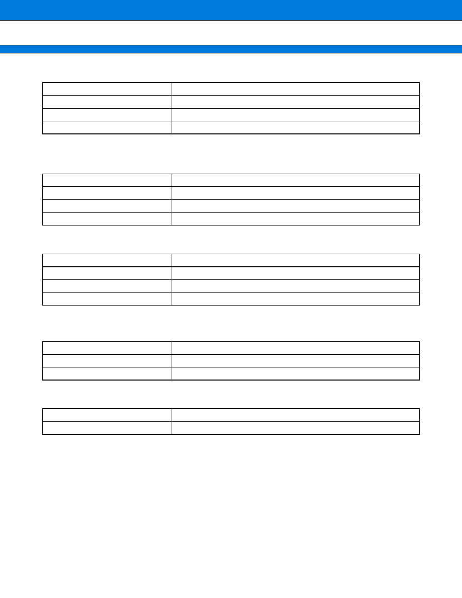
STANDARD CHARACTERISTICS
*: The capacity of the built-in capacitor is 20±8 pF by standard.
10±4 pF and 30±8 pF types are also available. However, the characteristics of 10±4 pF and 30±8 pF types are specified by
Fujitsu, considering matching data with applied IC (mainly microcomputer).
Series
C1 series
C3 series
C4 series
Parameter
Material
Lithium Tantalate (LiTaO
3
)
Lithium Niobate (LiNbO
3
)
Frequency
3.58 to 16 MHz
3 to 16 MHz
Standard frequency
See "
s
Standard frequency."
Initial frequency
tolerance
±0.05% (G)
±0.1% (J)
±0.3% (K)
±0.5% (M)
±0.1% (J)
±0.3% (K)
±0.5% (M)
±0.5% (M)
±0.3% (K)
±1% (L)
Temperature
characteristics
(≠20 to 60
∞
C)
±0.02%
±0.05%
±0.5%
Capacity of built-in
capacitor
--
20±8 pF (standard)*
Aging stability
Within ±0.1%
Operating temperature
≠30 to 85
∞
C
Storage temperature
≠40 to 100
∞
C
Standard measuring
circuit
R
30 pF
R:
Resonator
75
75
OSC
LM
(Resonant frequency and serial
resonant resistance)
3 MHz to 10 MHz max.
IC; 1/6MB84069B x 2
10 MHz to 16 MHz
IC; MC74HC04
V
CC
; 5 VDC
R; Resonator
C1, C2: Loading capacitors
(built-in)
R: Resonator
C
1
C
2
1 M
R
FAR
R
75
75
C
1
C
2
LM
(Serial resonant resistance)
(Oscillation frequency)
OSC

3
FAR Family (C1, C3, C4 series)
s
STANDARD FREQUENCY
∑
Package sizes and resonant resistance
There are two package sizes according to frequency:
For resonant resistance, standard values are specified according to frequency:
Note: For resonant resistance other than the standard values, they are specified by Fujitsu considering matching data with
applied IC (mainly micro computer).
s
NOTES ON USE
∑
Handle carefully.
∑
Solder under the following conditions.
CHIP type: 5 seconds max. at 230∞C (PCB)
SIP type: 10 seconds max. at 260∞C
Do not apply extreme heat to the resonator. Recommended preheating for the CHIP type is 150∞C for one
minute.
∑
Avoid extreme fluctuations in temperature during use.
∑
There is no specific direction in resonator mounting.
∑
Additional information is available separately, if required, for designing microcomputer oscillation circuits.
∑
CHIP type is for reflow solder, not for flow solder.
Standard
frequency (kHz)
C1/C3 series
C4 series
Package
size
Resonant
resistance
Package
size
Resonant
resistance
3,580
4,000
4,194
4,915
A
A
A
A
300
max.
(00)
A
A
A
A
150
max.
(01)
6,000
6,144
7,373
8,000
10,000
11,000
11,059
12,000
14,746
16.000
B
B
B
B
B
B
B
B
B
B
150
max.
(01)
B
B
B
B
B
B
B
B
B
B
75
max.
(02)
Frequency Package
size
3 to 5.99 MHz
A
6 to 16 MHz
B
Frequency
Standard resonant resistance
C1/C3 series
C4 series
3 to 3.57 MHz
--
300
max.
(00)
3.58 to 5.99 MHz
300
max.
(00)
150
max.
(01)
6 to 16 MHz
150
max.
(01)
75
max.
(02)

4
FAR Family (C1, C3, C4 series)
s
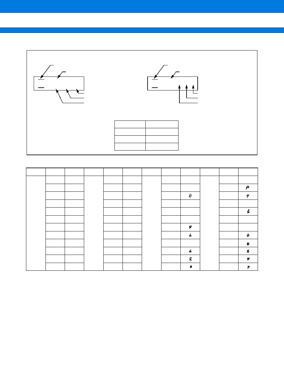
PART NUMBERING SYSTEM
(1) Series
(2) Package type
(3) Package size
See Table 1 in "
s
Dimensions."
(4) Frequency (kHz)
(5) Initial tolerance of frequency
See "
s
Standard Frequency."
Series
Single crystal
Capacitor
C1
LiTaO
3
--
C3
LiTaO
3
With built-in capacitors
C4
LiNbO
3
With built-in capacitors
Specification
Type
C
CHIP
S
SIP
Specification
Size
A
Large
B
Small
Frequency Designation Frequency Designation Frequency Designation Frequency Designation
3,580 kHz
03580
6,000 kHz
06000
10,000 kHz
10000
14,746 kHz
14746
4,000 kHz
04000
6,144 kHz
06144
11,000 kHz
11000
16,000 kHz
16000
4,194 kHz
04194
7,373 kHz
07373
11,059 kHz
11059
4,195 kHz
04915
8,000 kHz
08000
12,000 kHz
12000
Specification
Tolerance
C1 series
C3 series
C4 series
G
±0.05%
available
--
--
J
±0.1%
available
available
--
K
±0.3%
available
available
available
M
±0.5%
avaialble
available
available
L
±1%
--
--
available
(1)
FAR
(2)
(3)
(4)
(5)
(6)
(7)
(8)
5
FAR Family (C1, C3, C4 series)
(6) Capacity of built-in capacitor
Note: For C1 series, only "0" is available.
(7) Resonant resistance
(8) User-specific Special Symbols
(9)Taping specification
∑ SIP type
∑ CHIP type
Specification
Capacitance
0
20±8 pF
1
10±4 pF
2
30±8 pF
Specification
Resonant resistance
0
300
max.
1
150
max.
2
75
max.
Specification
Description
Name
No specification, no taping specification
--
No specification, with taping specification
A to Z
Serial number for custom design
Specification
Description
≠T
Reel pack
≠U
Ammo pack
Specification
Description
≠R
16 mm carrier pack
6
FAR Family (C1, C3, C4 series)
s
MARKING
Data code (EIAJ standard) is specified as follows in a four-year cycle.
Year
Month Symbol
Year
Month Symbol
Year
Month Symbol
Year
Month Symbol
1977
1981
1985
1989
1993
1
A
1978
1982
1986
1990
1994
1
N
1979
1983
1987
1991
1995
1
a
1980
1984
1988
1992
1996
1
n
2
B
2
P
2
b
2
3
C
3
Q
3
3
4
D
4
R
4
d
4
r
5
E
5
E
5
e
5
6
F
6
T
6
f
6
t
7
G
7
U
7
7
u
8
H
8
V
8
8
9
J
9
W
9
j
9
10
K
10
X
10
10
11
L
11
Y
11
11
12
M
12
Z
12
12
F
4000
T
k
m
Fujitsu's parts abbreviation
Frequency (kHz)
Lot No. (Date of manufacture,
conforms to EIAJ)
Initial frequency tolerance
Characteristics:
T: LiTaO
3
N: LiNbO
3
(SIP type)
F
1200
T
k
m
Fujitsu's parts abbreviation
Frequency (kHz)
Lot No. (Date of manufacture,
conforms to EIAJ)
Initial frequency tolerance
Characteristics:
T: LiTaO
3
N: LiNbO
3
(CHIP type)
The stamp color varies with the capacity of the capacitor.
Capacitance
Marking clolr
10 pF
Yellow
20 pF
White
30 pF
Gray

7
FAR Family (C1, C3, C4 series)
s
PIN ASSIGNMENT
3
∑
C1 series
SIP type
CHIP type
(Equivalent circuit)
∑
C3 and C4 series
SIP type
CHIP type
(Equivalent circuit)
1
2
3
1
2
1
2
1
2
3
1
2
1
2

8
FAR Family (C1, C3, C4 series)
s
DIMENSIONS
Table 1 Package size
Type
L
L
1
W
H
a
Two terminal
Three terminal
SIP type
A
11.0 ± 0.2
(0.433 ± 0.008)
--
4.3 ± 0.2
(0.169 ± 0.008)
6.3 ± 0.2
(0.248 ± 0.008)
5.08 ± 0.2
(0.200 ± 0.008)
2.54 ± 0.2
(0.100 ± 0.008)
B
9.0 ± 0.2
(0.354 ± 0.008)
--
4.3 ± 0.2
(0.169 ± 0.008)
5.3 ± 0.2
(0.209 ± 0.008)
CHIP type
A
10.0 ± 0.5
(0.394 ± 0.020)
9.4 ± 0.2
(0.370 ± 0.008)
4.5 ± 0.5
(0.177 ± 0.020)
2.5 ± 0.3
(0.098 ± 0.012)
B
8.0 ± 0.5
(0.315 ± 0.020)
7.4 ± 0.2
(0.291 ± 0.008)
3.2 ± 0.5
(0.126 ± 0.020)
2.5 ± 0.3
(0.098 ± 0.012)
H
W
L
a
0.5
±
0.2
(0.020
±
0.008)
0.35
±
0.1
(0.014
±
0.004)
3.4
±
0.2
(0.134
±
0.008)
H
W
L
a
0.5
±
0.2
(0.020
±
0.008)
0.35
±
0.1
(0.014
±
0.004)
3.4
±
0.2
(0.134
±
0.008)
a
C1 series
C3 and C4 series
SIP type
L
1
L
1
L
1
H
H
H
CHIP type
1.5
(0.059)
1.5
(0.059)
L
a
0.45
(0.018)
0.95
(0.037)
W
1.5
(0.059)
L
a
0.45
(0.018)
0.95
(0.037)
W
L
a
W
C1 series
C3 series
C4 series
a
a
Unit: mm (in.)

9
FAR Family (C1, C3, C4 series)
s
TAPING FORM AND DIMENSIONS
∑
SIP type
∑
CHIP type
Unit: mm (in.)
6.35
±
1.3
(0.250
±
0.051)
12.7
±
1.0
(0.500
±
0.394)
3.81
±
0.7
(0.150
±
0.028)
18.0
±
0.5
(0.709
±
0.020)
12.7
±
0.3
(0.500
±
0.012)
4.0
±
0.3 (0.157
±
0.012)
9.0
±
2
(0.354
±
0.079)
3.0 max. (0.118)
12.5 min.
(0.492)
18.0
+1.0
≠0.5
(0.709
)
+0.040
≠0.020
Note:
1. In reel packs, the tolerance of the cumulative feed hole pitch (20 pitches) is ±1.3 (0.051) or less.
2. In ammo packs, there must be perforations every 25 pitches.
Designation
Pack form
Pack quantity (pcs)
Package size A
Package size B
T
Reel pack
1000
1000
U
Ammo pack
1500
1500
4
±
0.1
(0.157
±
0.004)
2
±
0.1
(0.079
±
0.004)
±
0.1 (0.004)
8
±
0.15
(0.315
±
0.006)
3.0
±
0.1
(0.118
±
0.004)
W
±
0.1
(0.004)
6.85 (0.270)
1.5
±
0.1
(0.059
±
0.004)
Reel form
2.0 (0.080)
13.0
(0.512)
21.0
(0.827)
1.0
(0.039)
330
±
2.0
(12.992
±
0.079)
2.0 (0.079)
18.0 (0.709)
75 (2.953)
7.65
±
0.1
16
±
0.2
(0.630
±
0.008)
(0.301
±
0.004)
Unit: mm (in.)
Package
size
W
A
4.9
(0.193)
10.4
(0.409)
B
3.6
(0.142)
8.4
(0.331)
∑ Pack quantity
Package size
Pack
quantity
A
3,000 pcs
B
3,400 pcs

10
FAR Family (C1, C3, C4 series)
s
APPLICATION EXAMPLES
∑
C1 series
∑
C3, C4 series
s
RELIABILITY
Parameter
Test conditions
Requirements
Shock
MIL-STD-883B, 2002, condtion C (3000G)
Frequency fluctuation:
within ±0.1%
Vibration
MIL-STD-202E, 201A (1.5 mm <0.059> at 10 Hz
to 55 Hz for 2 hours)
Frequency fluctuation:
within ±0.1%
Drop
5 times drop from 1 m (39.370 in.) height to
wooden board.
Frequency fluctuation:
within ±0.1%
Sealing
Immersion in water at 85∞C
No bubbles observed
Heat resistance
MIL-STD-202E, 210A condition B (260∞C
∑
5 sec.)
Frequency fluctuation:
within ±0.1%
Temperature cycling
MIL-STD-883B, 1010, condition A (≠35 to 85∞C,
10 cycle)
Frequency fluctuation:
within ±0.1%
High-temperature loading test
MIL-STD-883B, 1008, condition B 1000 h (100∞C
∑
1000 hours)
Frequency fluctuation:
within ±0.1%
High-temperature humidity test
MIL-STD-202E, 103A, condition B (96 hours at
60∞C, 90% to 95% RH, 12 VDC)
Frequency fluctuation:
within ±0.1%
R
680
IC
IC
1.8 k
220
Output
22 pF to 47 pF
R: Resonator
IC: MB74LS04
TTL oscillation circuit
(serial resonation circuit)
1
R
2
MB8850
MB8850H series
2
1
3
R: Resonator

FAR Family (C1, C3, C4 series)
FUJITSU LIMITED
For further information please contact:
Japan
FUJITSU MEDIA DEVICES LIMITED
Marketing and Technical Support Dept.
SHINYOKOHAMA SQUARE BLDG
2-3-12,Shin-yokohama,
Kouhoku-ku, Yokohama-shi,
Kanagawa 222-0033, Japan
Tel: +81-45-471-0067
Fax: +81-45-471-0069
http://www.fujitsu.co.jp/hypertext/fmd/English/index.html
North and South America
FUJITSU MICROELECTRONICS, INC.
3545 North First Street,
San Jose, CA 95134-1804, U.S.A.
Tel: +1-408-922-9000
Fax: +1-408-922-9179
Customer Response Center
Mon. - Fri.: 7 am - 5 pm (PST)
Tel: +1-800-866-8608
Fax: +1-408-922-9179
http://www.fujitsumicro.com/
Europe
FUJITSU MICROELECTRONICS EUROPE GmbH
Am Siebenstein 6-10,
D-63303 Dreieich-Buchschlag,
Germany
Tel: +49-6103-690-0
Fax: +49-6103-690-122
http://www.fujitsu-fme.com/
Asia Pacific
FUJITSU MICROELECTRONICS ASIA PTE. LTD.
#05-08, 151 Lorong Chuan,
New Tech Park,
Singapore 556741
Tel: +65-281-0770
Fax: +65-281-0220
http://www.fmap.com.sg/
F9703
©
FUJITSU LIMITED Printed in Japan
All Rights Reserved.
The contents of this document are subject to change without notice.
Customers are advised to consult with FUJITSU sales
representatives before ordering.
The information and circuit diagrams in this document are
presented as examples of semiconductor device applications, and
are not intended to be incorporated in devices for actual use. Also,
FUJITSU is unable to assume responsibility for infringement of
any patent rights or other rights of third parties arising from the use
of this information or circuit diagrams.
The contents of this document may not be reproduced or copied
without the permission of FUJITSU LIMITED.
FUJITSU semiconductor devices are intended for use in standard
applications (computers, office automation and other office
equipments, industrial, communications, and measurement
equipments, personal or household devices, etc.).
CAUTION:
Customers considering the use of our products in special
applications where failure or abnormal operation may directly
affect human lives or cause physical injury or property damage, or
where extremely high levels of reliability are demanded (such as
aerospace systems, atomic energy controls, sea floor repeaters,
vehicle operating controls, medical devices for life support, etc.)
are requested to consult with FUJITSU sales representatives before
such use. The company will not be responsible for damages arising
from such use without prior approval.
Any semiconductor devices have inherently a certain rate of failure.
You must protect against injury, damage or loss from such failures
by incorporating safety design measures into your facility and
equipment such as redundancy, fire protection, and prevention of
over-current levels and other abnormal operating conditions.
If any products described in this document represent goods or
technologies subject to certain restrictions on export under the
Foreign Exchange and Foreign Trade Control Law of Japan, the
prior authorization by Japanese government should be required for
export of those products from Japan.