DS04-23116-2E
FUJITSU MEDIA DEVICE
DATA SHEET
ASSP Mobile Communication Systems
SAW Duplexer
(700 to 1000 MHz)
D5CC Series (D1)
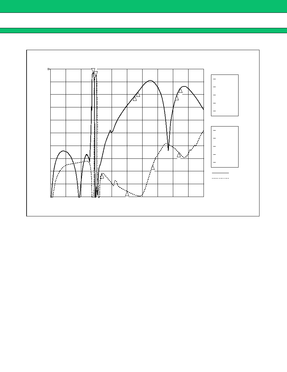
s
s
s
s
DESCRIPTION
The D5CC series of SAW antenna duplexer apply to the frequency range 700 to 1000 MHz.
The SAW filters are fabricated on a piezoelectric-crystal unit (LiTaO
3
:lithium tantalate) with a large electrome-
chanical dissociation.
The D5CC series provides small size and light duplexer by using original design, mounting and electrode formation
techniques.
D5CC(D1) series are incorporated transmitter filter and receiver filter into a small package and are housed phase
circuit in the package. Moreover, I/O of SAW filter is set to impedance 50
, so application requires no external
circuits.
s
s
s
s
FEATURES
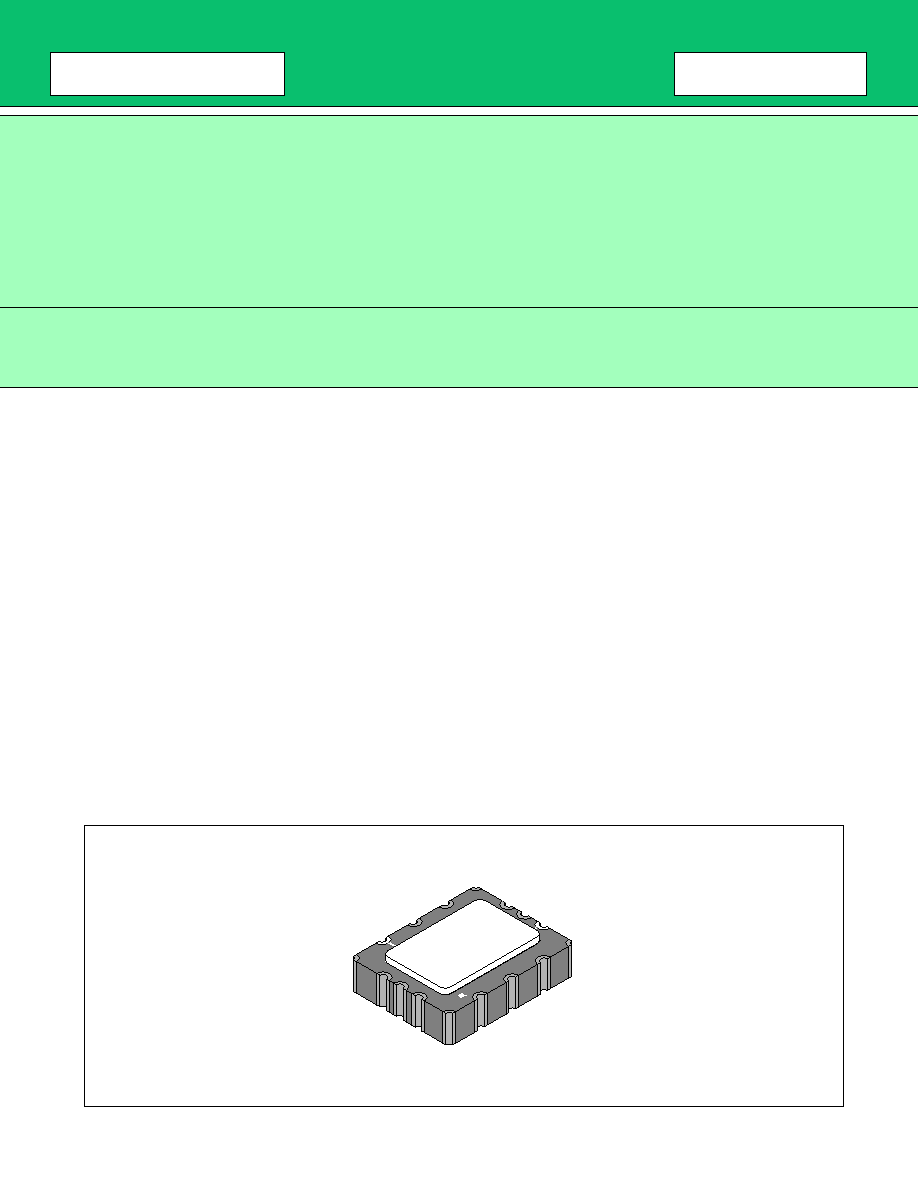
∑ Ultra compact and light package (0.14cm
3
, 9.5
◊
7.5
◊
2.0 (h) mm Typ.)
∑ External matching circuits are not required.
∑ Surface mount package (SMT)
∑ High handling power resistance (1.2 W Max.)
s
s
s
s
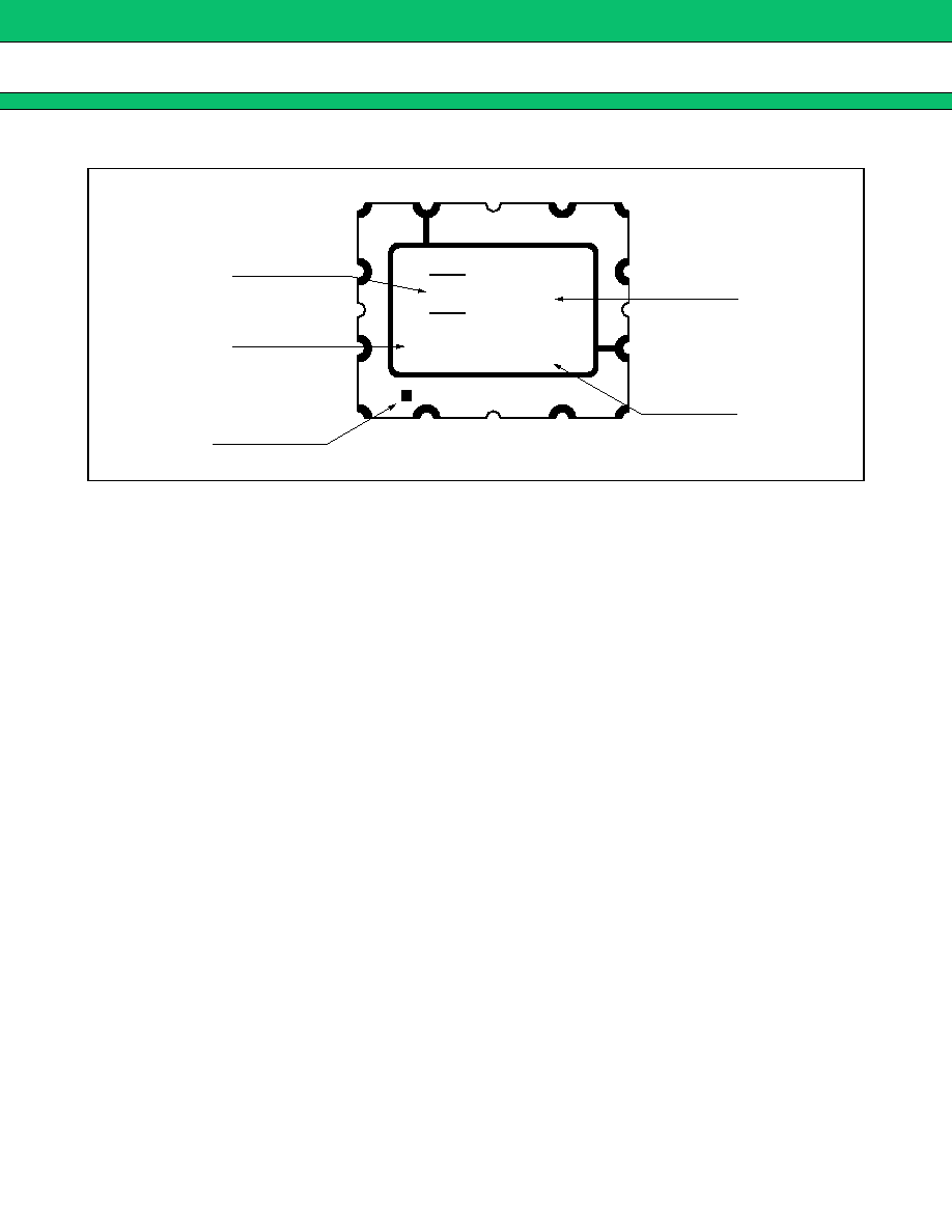
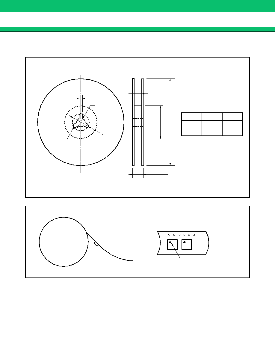
PACKAGE

D5CC Series (D1)
4
s
s
s
s
ABSOLUTE MAXIMUM RATINGS
WARNING: Piezoelectric devices can be permanently damaged by application of stress (voltage, current,
temperature, etc.) in excess of absolute maximum ratings. Do not exceed these ratings.
s
s
s
s
RECOMMENDED OPERATING CONDITIONS
WARNING: The recommended operating conditions are required in order to ensure the normal operation of the
piezoelectric device. All of the device's electrical characteristics are warranted when the device is
operated within these ranges.
Always use piezoelectric devices within their recommended operating condition ranges. Operation
outside these ranges may adversely affect reliability and could result in device failure.
No warranty is made with respect to uses, operating conditions, or combinations not represented on
the data sheet. Users considering application outside the listed conditions are advised to contact their
FUJITSU representatives beforehand.
s
s
s
s
STANDARD FREQUENCIES
Parameter
Symbol
Rating
Unit
Min.
Max.
Operating temperature
Ta
-
30
+
85
∞
C
Storage temperature
Tstg
-
40
+
100
∞
C
Maximum input power
P
IN
1.2
W
Input DC voltage
-
5
+5
V
Parameter
Symbol
Value
Unit
Min.
Max.
Operating temperature
Ta
-
30
+
85
∞
C
System
Tx freq.
(MHz)
Rx freq.
(MHz)
Part number
Part
symbol
Remarks
AMPS/IS-95/IS-136
824 to 849
869 to 894
FAR-D5CC-881M50-D1C8
C8

D5CC Series (D1)
FUJITSU MEDIA DEVICES LIMITED
For further information please contact:
Japan
FUJITSU MEDIA DEVICES LIMITED
International Sales and Marketing Dept.
Sin-Yokohama Square Bldg.,14F,
Shin-Yokohama 2-3-12, Kouhoku-ku,
Yokohama-shi, Kanagawa 222-0033, Japan
Tel: +81-45-471-0061
Fax: +81-45-471-0076
http://www.fujitsu.co.jp/hypertext/fmd/English/index.html
North and South America
FUJITSU MICROELECTRONICS, INC.
3545 North First Street,
San Jose, CA 95134-1804, U.S.A.
Tel: +1-408-922-9000
Fax: +1-408-922-9179
Customer Response Center
Mon. - Fri.: 7 am - 5 pm (PST)
Tel: +1-800-866-8608
Fax: +1-408-922-9179
http://www.fujitsumicro.com/
Europe
FUJITSU MICROELECTRONICS EUROPE GmbH
Am Siebenstein 6-10,
D-63303 Dreieich-Buchschlag,
Germany
Tel: +49-6103-690-0
Fax: +49-6103-690-122
http://www.fujitsu-fme.com/
Asia Pacific
FUJITSU MICROELECTRONICS ASIA PTE. LTD.
#05-08, 151 Lorong Chuan,
New Tech Park,
Singapore 556741
Tel: +65-281-0770
Fax: +65-281-0220
http://www.fmap.com.sg/
F0010
©
FUJITSU LIMITED Printed in Japan
All Rights Reserved.
The contents of this document are subject to change without notice.
Customers are advised to consult with FUJITSU sales
representatives before ordering.
The information and circuit diagrams in this document are
presented as examples of semiconductor device applications, and
are not intended to be incorporated in devices for actual use. Also,
FUJITSU is unable to assume responsibility for infringement of
any patent rights or other rights of third parties arising from the use
of this information or circuit diagrams.
The contents of this document may not be reproduced or copied
without the permission of FUJITSU LIMITED.
FUJITSU semiconductor devices are intended for use in standard
applications (computers, office automation and other office
equipments, industrial, communications, and measurement
equipments, personal or household devices, etc.).
CAUTION:
Customers considering the use of our products in special
applications where failure or abnormal operation may directly
affect human lives or cause physical injury or property damage, or
where extremely high levels of reliability are demanded (such as
aerospace systems, atomic energy controls, sea floor repeaters,
vehicle operating controls, medical devices for life support, etc.)
are requested to consult with FUJITSU sales representatives before
such use. The company will not be responsible for damages arising
from such use without prior approval.
Any semiconductor devices have inherently a certain rate of failure.
You must protect against injury, damage or loss from such failures
by incorporating safety design measures into your facility and
equipment such as redundancy, fire protection, and prevention of
over-current levels and other abnormal operating conditions.
If any products described in this document represent goods or
technologies subject to certain restrictions on export under the
Foreign Exchange and Foreign Trade Control Law of Japan, the
prior authorization by Japanese government should be required for
export of those products from Japan.