THE POSSIBILITIES ARE INFINITE
THE POSSIBILITIES ARE INFINITE
Customer Name
STANDARD
FUJITSU MEDIA DEVICES LIMITED
System
AMPS/CDMA/TDMA SAW Duplexer
DATE
Mar.26.2003
FMD P/N
FAR-D5CM-881M50-D1G1 Version
2.0b
Preliminary
Customer P/N
Reference No.
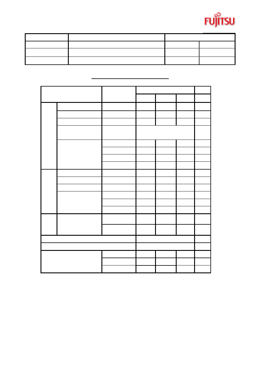
Table 1 Electrical Specification
FMD Current proposal
Unit
Condition
Min
Typ.
Max
Insertion loss
824-849MHz
-
2.0
2.5
dB
Pass band ripple
824-849MHz
-
0.8
1.3
dB
Pass band VSWR
824-849MHz
-
2.0
2.2
-
Input Power
824-849 MHz
1.2 W >50000 Hours
CW tone (Ta=+50
o
C)
Watt
779-804MHz 20 30 - dB
869-894MHz 40 43 - dB
1648-1698MHz
35 40 - dB
Tx
to
ANT
Attenuation
2472-2547MHz
13 15 - dB
Insertion loss
869-894MHz
-
2.5 3.3 dB
Pass band ripple
869-894MHz
-
1.0
1.5
dB
Pass band VSWR
869-894MHz
-
2.0
2.3
-
824-849MHz 50 53 - dB
930-1200MHz 35 38 - dB
ANT
to
Rx
Attenuation
1200-1800MHz
35 38 - dB
824-849 MHz
54
57
dB
Tx
to
Rx
Isolation
869-894 MHz
45
47
-
dB
Storage Temperature
-40 to +100
o
C
Operating Temperature
-30 to +85
o
C
Length -
5.0
5.2
mm
Width -
5.0
5.2
mm
Package size
Height -
1.5
1.7
mm

THE POSSIBILITIES ARE INFINITE
THE POSSIBILITIES ARE INFINITE
Customer Name
STANDARD
FUJITSU MEDIA DEVICES LIMITED
System
AMPS/CDMA/TDMA SAW Duplexer
DATE
Mar.26.2003
FMD P/N
FAR-D5CM-881M50-D1G1 Version
2.0b
Preliminary
Customer P/N
Reference No.
Dimensions and Pin assignment
0.
1
0.
1
05+
/-
05+
/-
5.
5.
5.05+/-0.1
Pin 1 Index
F
G1
ANT
Tx Rx
1.5
(1.7 Max.)
ALL DIMENSIONS IN mm
0
.
6+
/
-
0.
15
1.3
+
/
-
0.
15
4-R0.2
12-R0.2
0.6+/-0.15
0.6
5
/
-
0.
15
1.27
1.2
7
0.65+/-0.15
TOP VIEW
SIDE VIEW
BOTTOM VIEW
10
11
12
7 8 9
3 2 1
6
5
4
5.05+/-0.1
Pin 1 Index
F
G1
ANT
Tx Rx
1.5
(1.7 Max.)
ALL DIMENSIONS IN mm
0
.
6+
/
-
0.
15
1.3
+
/
-
0.
15
4-R0.2
12-R0.2
0.6+/-0.15
0.6
5
/
-
0.
15
1.27
1.2
7
0.65+/-0.15
0
.
6+
/
-
0.
15
0
.
6+
/
-
0.
15
1.3
+
/
-
0.
15
4-R0.2
12-R0.2
0.6+/-0.15
0.6
5
/
-
0.
15
1.27
1.27
1.2
7
1.2
7
0.65+/-0.15
TOP VIEW
SIDE VIEW
BOTTOM VIEW
10
11
12
7 8 9
3 2 1
6
5
4
Pin No.
Pin name
Description
1 GND
Ground
Pin
2 GND
Ground
Pin
3 GND
Ground
Pin
4 GND
Ground
Pin
5 Rx
Receiver
Pin
6 GND
Ground
Pin
7 GND
Ground
Pin
8 ANT
Antenna
Pin
9 GND
Ground
Pin
10 GND
Ground
Pin
11 Tx Transmitter
Pin
12 GND
Ground
Pin

THE POSSIBILITIES ARE INFINITE
THE POSSIBILITIES ARE INFINITE
Customer Name
STANDARD
FUJITSU MEDIA DEVICES LIMITED
System
AMPS/CDMA/TDMA SAW Duplexer
DATE
Mar.26.2003
FMD P/N
FAR-D5CM-881M50-D1G1 Version
2.0b
Preliminary
Customer P/N
Reference No.
Evaluation Circuit
Ant port
Tx port Rx port
1,2,3,4,6,
7,9,10,12
8
11 5
1~12:Pin No.
GND
Recommended foot print pattern
PRELIMINARY
1.2 7
1.2 7
5
.
0
1
.
4
5 .0
1
2
-
0
.
3
0
.
7
0
.
7
Version 1.1
Isolated pad layout
9 8 7
1 2 3
10
11
12
6
5
4
0.5
0.
5
0.5
0.5
0.
5
0.
5
Pin No.
Symbol
Function
1
GND
Ground
2
GND
Ground
3
GND
Ground
4
GND
Ground
5
Rx
Receiver
6
GND
Ground
7
GND
Ground
8
ANT
Antenna
9
GND
Ground
10
GND
Ground
11
Tx
Transmitter
12
GND
Ground
Common Ground layout
9 8 7
1 2 3
10
11
12
6
5
4
All Dimension in mm
PRELIMINARY
1.2 7
1.2 7
5
.
0
1
.
4
5 .0
1
2
-
0
.
3
0
.
7
0
.
7
Version 1.1
Isolated pad layout
9 8 7
1 2 3
10
11
12
6
5
4
0.5
0.5
0.
5
0.
5
0.5
0.5
0.5
0.5
0.
5
0.
5
0.
5
0.
5
Pin No.
Symbol
Function
1
GND
Ground
2
GND
Ground
3
GND
Ground
4
GND
Ground
5
Rx
Receiver
6
GND
Ground
7
GND
Ground
8
ANT
Antenna
9
GND
Ground
10
GND
Ground
11
Tx
Transmitter
12
GND
Ground
Common Ground layout
9 8 7
1 2 3
10
11
12
6
5
4
9 8 7
1 2 3
10
11
12
6
5
4
All Dimension in mm
THE POSSIBILITIES ARE INFINITE
THE POSSIBILITIES ARE INFINITE
Customer Name
STANDARD
FUJITSU MEDIA DEVICES LIMITED
System
AMPS/CDMA/TDMA SAW Duplexer
DATE
Mar.26.2003
FMD P/N
FAR-D5CM-881M50-D1G1 Version
2.0b
Preliminary
Customer P/N
Reference No.
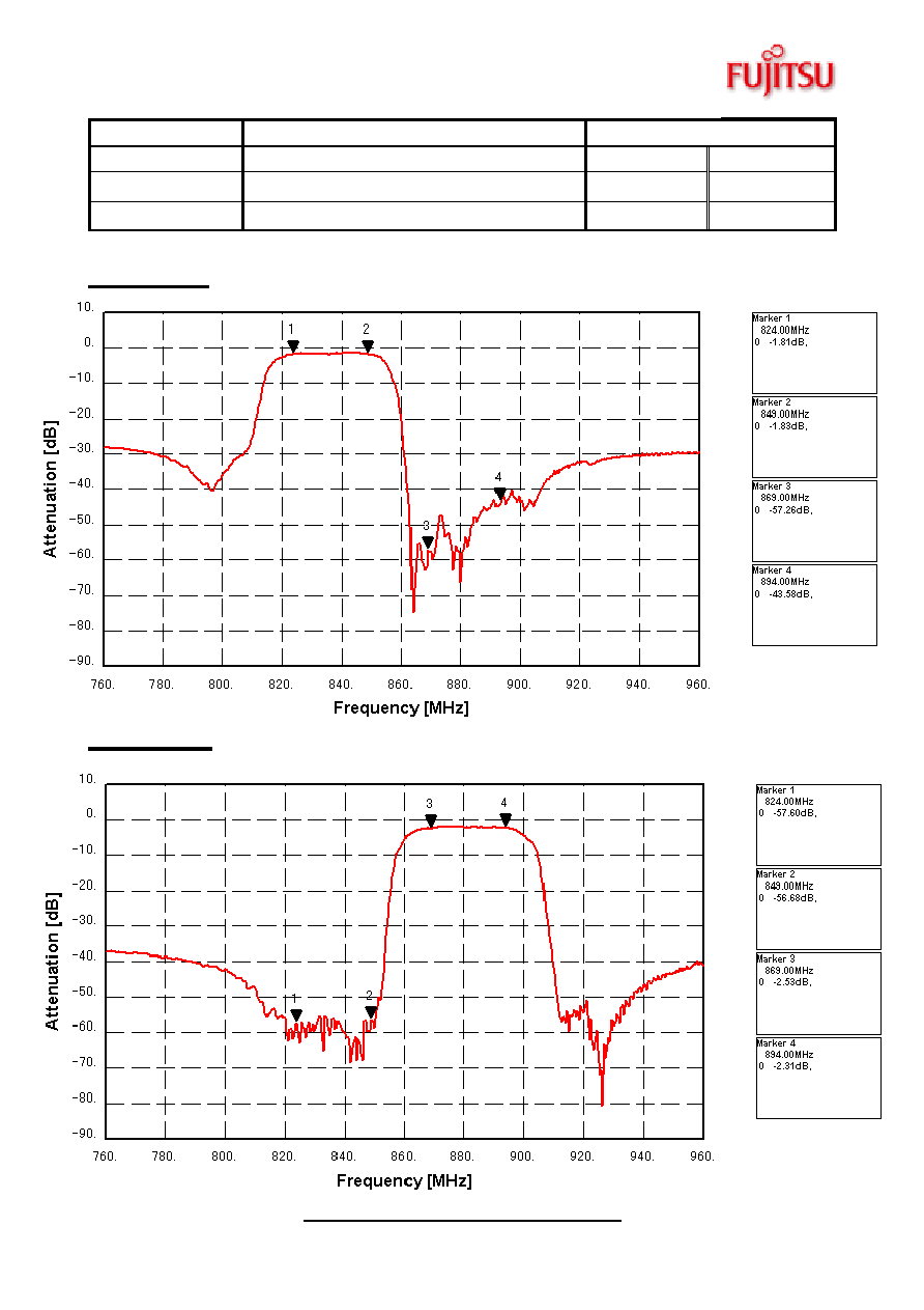
Tx to Ant
Ant to Rx
Figure 1-1 Electrical Characteristics

THE POSSIBILITIES ARE INFINITE
THE POSSIBILITIES ARE INFINITE
Customer Name
STANDARD
FUJITSU MEDIA DEVICES LIMITED
System
AMPS/CDMA/TDMA SAW Duplexer
DATE
Mar.26.2003
FMD P/N
FAR-D5CM-881M50-D1G1 Version
2.0b
Preliminary
Customer P/N
Reference No.
Tx to Rx Isolation
Figure 1-2 Electrical Characteristics