DS04-23118-1E
FUJITSU SEMICONDUCTOR
DATA SHEET
ASSP
Mobile Communication Systems
Piezoelectric SAW BPF
(700 to 1000 MHz)
F5CE Series (D2 type)
s
DESCRIPTION
The F5CE-D2 series of SAW bandpass filters apply to the frequency range 700 to 1000 MHz. These filters make
it possible to provide high stopband attenuation and excellent passband flatness due to using unique DMS (Double
Mode SAW) technology as design method. Moreover, these filters are provided in small 3.0 mm sq. package. This
contributes to reduce weight and size of mobile communication units.
The F5CE-D2 series of SAW filters are suitable for interstage RF filter in mobile communication systems in the
frequency range 700 to 1000 MHz. Standard devices are available for AMPS/CDMA/TDMA, GSM, PDC800 and
ISM900.
s
FEATURES
∑ Excellent stopband attenuation
∑ Low insertion loss and low passband ripple
∑ Ultra compact and light package (3.0 mm sq.)
∑ External matching circuits are not required. (50 ohms I/O)
∑ Surface mount package (SMT)
∑ Standard devices are available for mobile communication standards
(AMPS/CDMA/TDMA, GSM, PDC800 and ISM900)
s
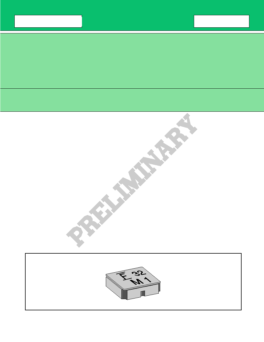
PACKAGE
2
F5CE Series (D2 type)
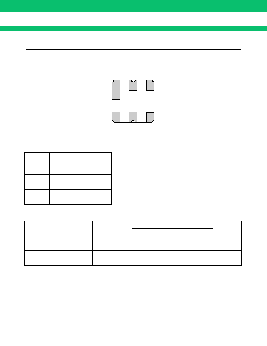
s
PIN ASSIGNMENT
s
PIN DESCRIPTION
s
ABSOLUTE MAXIMUM RATINGS
WARNING: Piezoelectric devices can be permanently damaged by application of stress (voltage, power,
temperature, etc.) in excess of absolute maximum ratings. Do not exceed these ratings.
Pin no.
Pin name
Description
1
GND
Ground Pin
2
IN
Input Pin
3
GND
Ground Pin
4
GND
Ground Pin
5
OUT
Output Pin
6
GND
Ground Pin
Parameter
Symbol
Rating
Unit
Min.
Max.
Operating temperature
Ta
≠30
+85
∞
C
Storage temperature
Tstg
≠40
+100
∞
C
Input power
P
IN
≠
+15
dBm
Input DC voltage
DC
≠5
+5
V
(BOTTOM VIEW)
1
2
3
6
5
4
3
F5CE Series (D2 type)
s
RECOMMENDED OPERATING CONDITION
WARNING: Recommended operating conditions are normal operating ranges for the piezoelectric device. All the
device's electrical characteristics are warranted when operated within these ranges.
Always use piezoelectric devices within the recommended operating conditions. Operation outside
these ranges may adversely affect reliability and could result in device failure.
No warranty is made with respect to uses, operating conditions, or combinations not represented on
the data sheet. Users considering application outside the listed conditions are advised to contact their
FUJITSU representative beforehand.
s
STANDARD FREQUENCIES
Parameter
Symbol
Value
Unit
Min.
Max.
Operating temperature
Ta
≠30
+85
∞
C
System
Center freq.
(MHz)
B/W
(MHz)
Part
symbol
Part number
Remarks
PDC800
Tx
950.0
20
30
FAR-F5CE-950M00-D230
Rx
820.0
20
31
FAR-F5CE-820M00-D231
AMPS
/CDMA
/TDMA
836.5
25
32
FAR-F5CE-836M50-D232
Rx
881.5
25
33
FAR-F5CE-881M50-D233
GSM/NMT
Tx
902.5
25
34
FAR-F5CE-902M50-D234
Rx
947.5
25
35
FAR-F5CE-947M50-D235
ISM900
--
915.0
7
38
FAR-F5CE-915M00-D238
Tx
4
F5CE Series (D2 type)
s
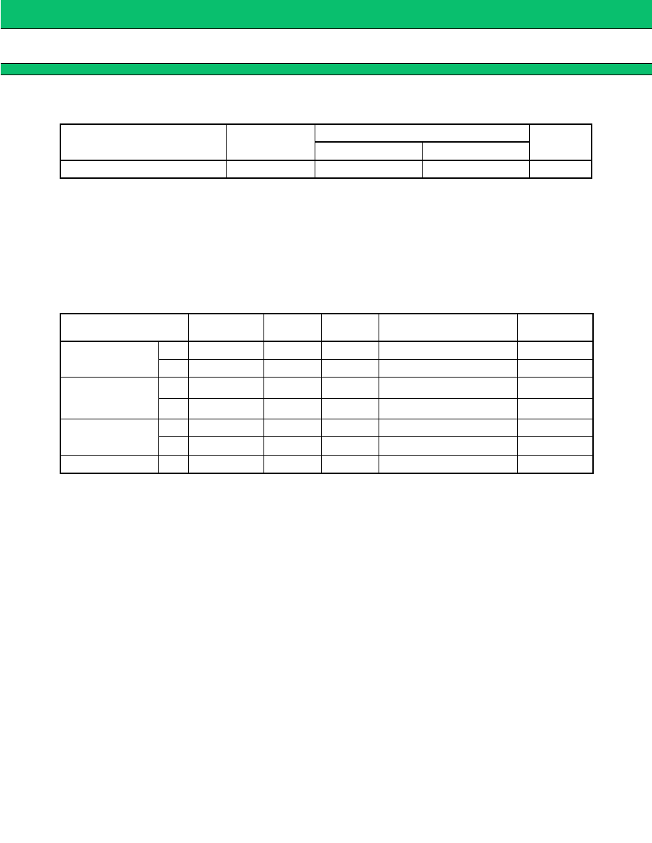
ELECTRICAL CHARACTERISTICS
1. PDC800 (Tx)
Part number: FAR-F5CE-950M00-D230
(Ta = ≠30 to +85
∞
C)
2. PDC800 (Rx)
Part number: FAR-F5CE-820M00-D231
(Ta = ≠30 to +85
∞
C)
Parameter
Symbol
Conditions
Value
Unit
Remarks
Min.
Typ.
Max.
Insertion loss
IL
940 to 960 MHz
--
2.6
3.0
dB
Inband ripple
--
940 to 960 MHz
--
0.7
1.2
dB
Absolute
attenuation
--
DC to 680 MHz
50
66
--
dB
--
680 to 696 MHz
50
69
--
dB
--
810 to 830 MHz
50
66
--
dB
--
1015 to 1106 MHz
35
42
--
dB
--
1106 to 1700 MHz
50
59
--
dB
--
1700 to 2000 MHz
40
59
--
dB
Inband VSWR
--
940 to 960 MHz
--
1.8
2.0
--
Parameter
Symbol
Conditions
Value
Unit
Remarks
Min.
Typ.
Max.
Insertion loss
IL
810 to 830 MHz
--
2.5
3.0
dB
Inband ripple
--
810 to 830 MHz
--
0.7
1.2
dB
Absolute
attenuation
--
DC to 760 MHz
50
65
--
dB
--
855 to 875 MHz
28
30
--
dB
--
875 to 920 MHz
35
38
--
dB
--
920 to 1200 MHz
45
60
--
dB
--
1200 to 2000 MHz
40
47
--
dB
Inband VSWR
--
810 to 830 MHz
--
1.7
2.0
--
5
F5CE Series (D2 type)
3. AMPS/CDMA/TDMA (Tx)
Part number: FAR-F5CE-836M50-D232
(Ta = ≠30 to +85
∞
C)
4. AMPS/CDMA/TDMA (Rx)
Part number: FAR-F5CE-881M50-D233
(Ta = ≠30 to +85
∞
C)
Parameter
Symbol
Conditions
Value
Unit
Remarks
Min.
Typ.
Max.
Insertion loss
IL
824 to 849 MHz
--
2.7
3.5
dB
Inband ripple
--
824 to 849 MHz
--
0.9
1.6
dB
Absolute
attenuation
--
DC to 800 MHz
50
66
--
dB
--
869 to 1049 MHz
28
33
--
dB
--
1049 to 1200 MHz
50
60
--
dB
--
1200 to 2000 MHz
45
50
--
dB
Inband VSWR
--
824 to 849 MHz
--
1.8
2.0
--
Parameter
Symbol
Conditions
Value
Unit
Remarks
Min.
Typ.
Max.
Insertion loss
IL
869 to 894 MHz
--
2.7
3.5
dB
Inband ripple
--
869 to 894 MHz
--
0.9
1.6
dB
Absolute
attenuation
--
DC to 779 MHz
50
63
--
dB
--
779 to 849 MHz
45
50
--
dB
--
914 to 970 MHz
28
33
--
dB
--
970 to 1049 MHz
50
60
--
dB
--
1049 to 2000 MHz
40
50
--
dB
Inband VSWR
--
869 to 894 MHz
--
1.7
2.0
--
6
F5CE Series (D2 type)
5. GSM/NMT (Tx)
Part number: FAR-F5CE-902M50-D234
(Ta = ≠30 to +85
∞
C)
6. GSM/NMT (Rx)
Part number: FAR-F5CE-947M50-D235
(Ta = ≠30 to +85
∞
C)
Parameter
Symbol
Conditions
Value
Unit
Remarks
Min.
Typ.
Max.
Insertion loss
IL
890 to 915 MHz
--
2.8
3.3
dB
Inband ripple
--
890 to 915 MHz
--
0.8
1.4
dB
Absolute
attenuation
--
DC to 845 MHz
50
60
--
dB
--
845 to 870 MHz
45
50
--
dB
--
925 to 935 MHz
5
18
--
dB
--
935 to 980 MHz
28
33
--
dB
--
980 to 1200 MHz
50
60
--
dB
--
1200 to 3000 MHz
30
40
--
dB
Inband VSWR
--
890 to 915 MHz
--
1.7
2.1
--
Parameter
Symbol
Conditions
Value
Unit
Remarks
Min.
Typ.
Max.
Insertion loss
IL
935 to 960 MHz
--
2.7
3.3
dB
Inband ripple
--
935 to 960 MHz
--
0.7
1.4
dB
Absolute
attenuation
--
DC to 871 MHz
50
66
--
dB
--
890 to 915 MHz
30
40
--
dB
--
980 to 1025 MHz
25
34
--
dB
--
1025 to 2000 MHz
45
48
--
dB
--
2000 to 3000 MHz
30
33
--
dB
Inband VSWR
--
935 to 960 MHz
--
1.9
2.1
--
7
F5CE Series (D2 type)
7. ISM900 (7 MHz Bandwidth)
Part number: FAR-F5CE-915M00-D238
(Ta = ≠30 to +85
∞
C)
Parameter
Symbol
Conditions
Value
Unit
Remarks
Min.
Typ.
Max.
Insertion loss
IL
911.5 to 918.5 MHz
--
3.2
3.5
dB
Inband ripple
--
911.5 to 918.5 MHz
--
0.3
1.0
dB
Absolute
attenuation
--
DC to 600 MHz
50
66
--
dB
--
600 to 840 MHz
40
35
--
dB
--
869 to 894 MHz
35
40
--
dB
--
970 to 1500 MHz
40
45
--
dB
--
1500 to 3000 MHz
25
28
--
dB
Inband VSWR
--
911.5 to 918.5 MHz
--
1.8
2.0
--
8
F5CE Series (D2 type)
s
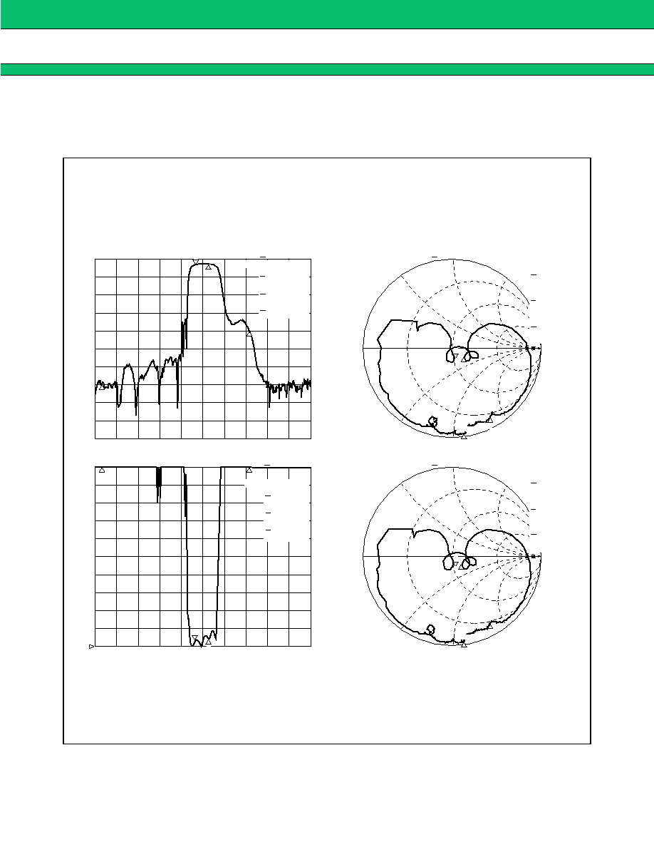
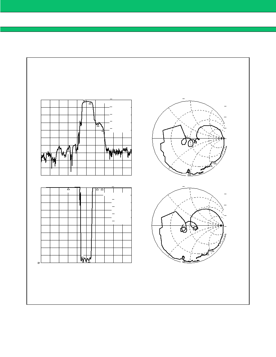
TYPICAL CHARACTERISTICS (STANDARD VERSION)
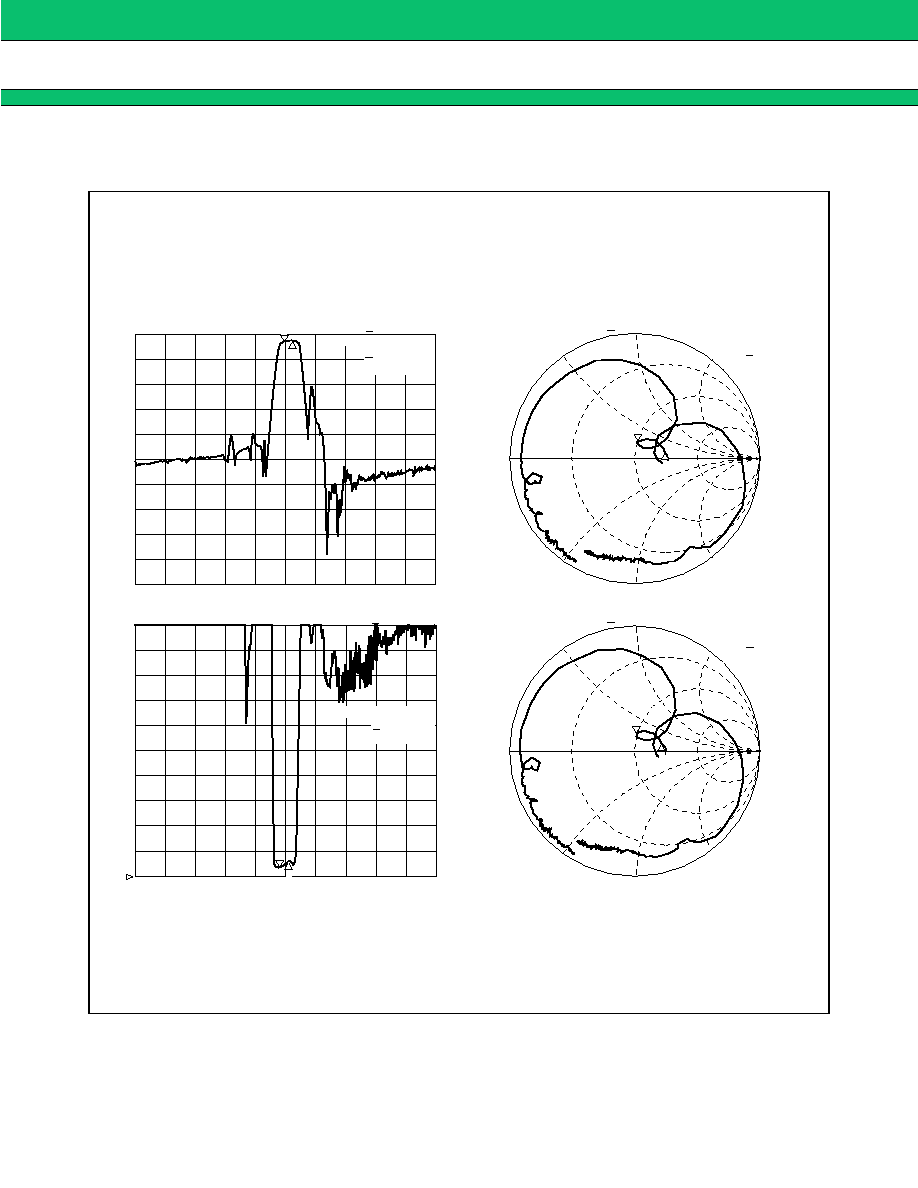
1. PDC800 (Tx)
Part number: FAR-F5CE-950M00-D230
3
2
1
S 21
log MAG
10 dB/
CENTER 0.950 000 000 GHz
SPAN 0.300 000 000 GHz
CENTER 0.950 000 000 GHz
SPAN 0.300 000 000 GHz
CENTER 0.950 000 000 GHz
SPAN 0.300 000 000 GHz
CENTER 0.950 000 000 GHz
SPAN 0.300 000 000 GHz
4
2
:
-
2.342 dB
0.9600 GHz
3
:
-
68.839 dB
0.8100 GHz
4
:
-
39.73 dB
1.0150 GHz
0.940 000 000 GHz
1
:
-
2.568 dB
CH1
C2
H1d
D
O
1
3
2
1
S 11
1 U FS
4
2
:
66.398
-
11.027
0.9600 GHz
3
:
2.0508
-
57.342
0.8100 GHz
4
:
12.441
-
84.324
1.0150 GHz
0.940 000 000 GHz
1
:
52.076
14.686 pF
-
11.529
CH1
C2
H1d
D
O
1
3
2
1
S 11
SWR
1 /
2
:
1.4082
0.9600 GHz
3
:
58.55
0.8100 GHz
4
:
15.631
1.0150 GHz
0.940 000 000 GHz
1
:
1.2585
CH1
C2
H1d
D
O
1
3
2
1
S 22
1 U FS
4
2
:
64.738
-
8.7813
0.9600 GHz
3
:
2.3711
-
56.83
0.8100 GHz
4
:
18.398
-
84.547
1.0150 GHz
0.940 000 000 GHz
1
:
51.699
15.105 pF
-
11.209
CH1
C2
H1d
D
O
1
4
REF 0 dB
REF 1
9
F5CE Series (D2 type)
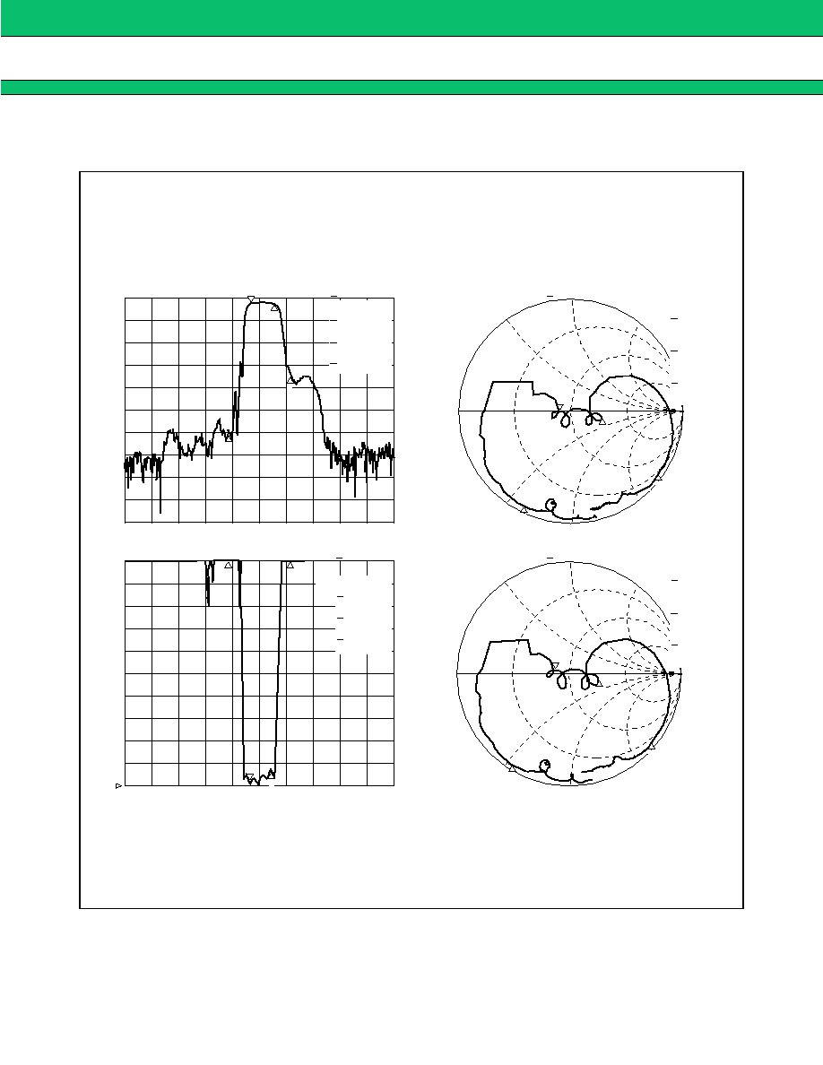
2. PDC800 (Rx)
Part number: FAR-F5CE-820M00-D231
3
2
S 21
log MAG
10 dB/
CENTER 0.820 000 000 GHz
SPAN 0.300 000 000 GHz
CENTER 0.820 000 000 GHz
SPAN 0.300 000 000 GHz
CENTER 0.820 000 000 GHz
SPAN 0.300 000 000 GHz
CENTER 0.820 000 000 GHz
SPAN 0.300 000 000 GHz
4
5
2
:
-
2.109 dB
0.8300 GHz
3
:
-
63.906 dB
0.7600 GHz
4
:
-
31.312 dB
1.0150 GHz
5
:
-
39.558 dB
1.0150 GHz
0.810 000 000 GHz
1
:
-
2.451 dB
CH1
C2
H1d
D
O
1
3
5
2
1
S 11
1 U FS
4
2
:
67.109
-
5.3945
0.8300 GHz
3
:
3.4922
-
49.041
0.7800 GHz
4
:
17.785
-
127.42
0.8550 GHz
5
:
15.277
-
100.98
0.8750 GHz
0.810 000 000 GHz
1
:
41.9
79.439 pF
0.4043
CH1
C2
H1d
D
O
1
3
2
1
S 11
SWR
1 /
2
:
1.3628
0.8300 GHz
3
:
28.125
0.7600 GHz
4
:
21.387
0.8550 GHz
5
:
21.387
0.8550 GHz
0.810 000 000 GHz
1
:
1.1981
CH1
C2
H1d
D
O
1
3
2
1
S 22
1 U FS
5
4
2
:
65.793
-
4.418
0.8300 GHz
3
:
3.6797
-
43.031
0.7600 GHz
4
:
18.219
-
120.1
0.8550 GHz
5
:
15.129
-
93.582
0.8750 GHz
0.810 000 000 GHz
1
:
37.752
47.32 pF
-
4.1523
CH1
C2
H1d
D
O
1
4
5
REF 0 dB
REF 1
1
10
F5CE Series (D2 type)
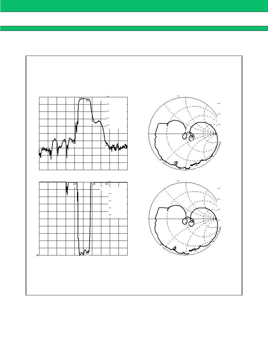
3. AMPS/CDMA/TDMA (Tx)
Part number: FAR-F5CE-836M50-D232
3
2
1
S 21
log MAG
10 dB/
CENTER 835.000 000 MHz
SPAN 300.000 000 MHz
CENTER 835.000 000 MHz
SPAN 300.000 000 MHz
CENTER 835.000 000 MHz
SPAN 300.000 000 MHz
CENTER 835.000 000 MHz
SPAN 300. 000 000 GHz
4
2
:
-
2.7135 dB
849 MHz
3
:
-
60.88 dB
800 MHz
4
:
-
34.243 dB
869 MHz
824.000 000 MHz
1
:
-
2.643 dB
CH1
Cor
H1d
D
O
1
3
2
1
S 11
1 U FS
4
2
:
84.996
-
12.77
849 MHz
3
:
2.0156
-
29.858
800 MHz
4
:
18.031
-
140.37
869 MHz
824.00 000 MHz
1
:
39.861
18.108 pF
0.0938
CH1
Cor
H1d
D
O
1
3
2
1
S 11
SWR
1 /
2
:
1.7589
849 MHz
3
:
33.646
800 MHz
4
:
34.335
869 MHz
824.000 000 MHz
1
:
1.2555
CH1
Cor
H1d
D
O
1
3
2
1
S 22
1 U FS
4
2
:
84.547
-
10.078
849 MHz
3
:
2.1123
-
88.005
800 MHz
4
:
12.773
-
134.22
869 MHz
824.000 000 MHz
1
:
40.059
458.73 pF
2.375
CH1
Cor
H1d
D
O
1
4
REF 0 dB
REF 1

11
F5CE Series (D2 type)
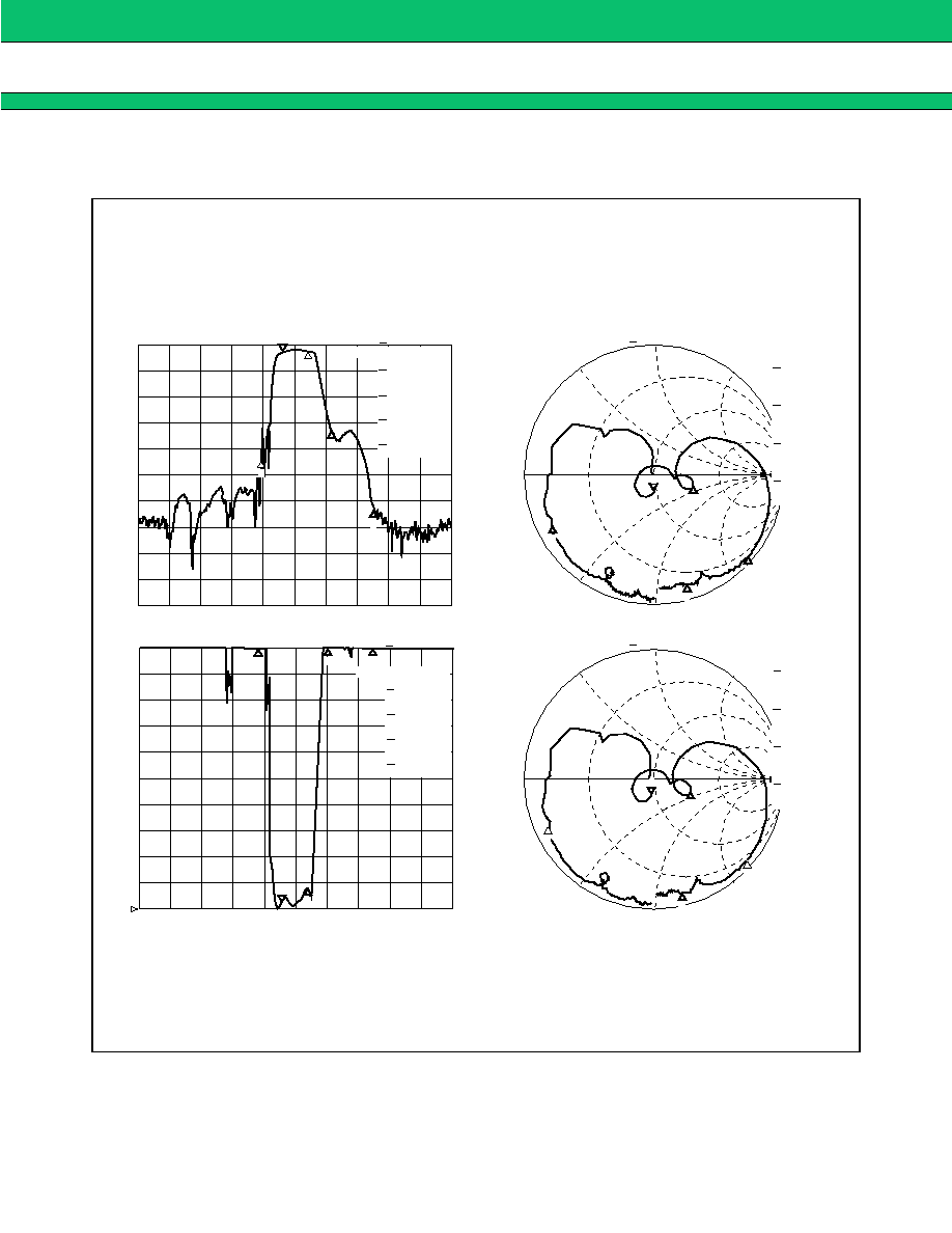
4. AMPS/CDMA/TDMA (Rx)
Part number: FAR-F5CE-881M50-D233
3
2
1
S 21
log MAG
10 dB/
CENTER 880.000 000 MHz
SPAN 300.000 000 MHz
CENTER 880.000 000 MHz
SPAN 300.000 000 MHz
CENTER 880.000 000 MHz
SPAN 300.000 000 MHz
CENTER 880.000 000 MHz
SPAN 300. 000 000 GHz
4
2
:
-
2.7063 dB
894 MHz
3
:
-
62.398 dB
849 MHz
4
:
-
33.178 dB
914 MHz
869.000 000 MHz
1
:
-
2.6219 dB
CH1
Cor
H1d
D
O
1
3
2
1
S 11
1 U FS
4
2
:
89.652
-
9.0273
894 MHz
3
:
2.2881
-
23.078
849 MHz
4
:
16.703
-
149.05
914 MHz
869.00 000 MHz
1
:
48.748
107.05 pF
-
1.7109
CH1
Cor
H1d
D
O
1
3
2
1
S 11
SWR
1 /
2
:
1.8203
894 MHz
3
:
26.584
849 MHz
4
:
31.784
914 MHz
869.000 000 MHz
1
:
1.0512
CH1
Cor
H1d
D
O
1
3
2
1
S 22
1 U FS
4
2
:
88.297
-
7.6133
894 MHz
3
:
2..3965
-
21.153
849 MHz
4
:
14.922
-
139.78
914 MHz
869.000 000 MHz
1
:
48.572
277.43 pF
-
660.16 m
CH1
Cor
H1d
D
O
1
4
REF 0 dB
REF 1
12
F5CE Series (D2 type)
5. GSM/NMT (Tx)
Part number: FAR-F5CE-902M50-D234
2
1
S 21
log MAG
10 dB/
CENTER 0.900 000 000 GHz
SPAN 0.300 000 000 GHz
CENTER 0.900 000 000 GHz
SPAN 0.300 000 000 GHz
CENTER 0.900 000 000 GHz
SPAN 0.300 000 000 GHz
CENTER 0.900 000 000 GHz
SPAN 0.300 000 000 GHz
5
2
:
-
2.512 dB
0.9150 GHz
3
:
-
60.125 dB
0.8690 GHz
4
:
-
32.472 dB
0.9350 GHz
5
:
-
63.11 dB
0.9800 GHz
0.890 000 000 GHz
1
:
-
2.705 dB
CH1
C2
H1d
D
O
1
3
5
S 11
1 U FS
4
2
:
73.234
-
8.75
0.9150 GHz
3
:
2.377
-
21.645
0.8690 GHz
4
:
16.141
-
154.23
0.9350 GHz
5
:
9.9835
-
71.762
0.9800 GHz
0.890 000 000 GHz
1
:
54.355
54.499 pF
-
3.2813
CH1
C2
H1d
D
O
1
3
2
1
S 11
SWR
1 /
2
:
1.5029
0.9150 GHz
3
:
25.029
0.8690 GHz
4
:
32.898
0.9350 GHz
5
:
15.535
0.9800 GHz
0.890 000 000 GHz
1
:
1.1118
CH1
C2
H1d
D
O
1
5
3
S 22
1 U FS
2
:
72.748
-
8.6719
0.9150 GHz
3
:
2.3945
-
20.338
0.8690 GHz
4
:
14.781
-
143.07
0.9350 GHz
5
:
9.7883
-
88.281
0.9800 GHz
0.890 000 000 GHz
1
:
54.16
74.925 pF
-
2.3867
CH1
C2
H1d
D
O
1
4
5
REF 0 dB
REF 1
3
2
1
2
1
4
4
13
F5CE Series (D2 type)
6. GSM/NMT (Rx)
Part number: FAR-F5CE-947M50-D235
3
2
1
S 21
log MAG
10 dB/
CENTER 0.950 000 000 GHz
SPAN 0.300 000 000 GHz
CENTER 0.950 000 000 GHz
SPAN 0.300 000 000 GHz
CENTER 0.950 000 000 GHz
SPAN 0.300 000 000 GHz
CENTER 0.950 000 000 GHz
SPAN 0.300 000 000 GHz
4
5
2
:
-
2.811 dB
0.9600 GHz
3
:
-
43.265 dB
0.9150 GHz
4
:
-
31.174 dB
0.9800 GHz
5
:
-
62.902 dB
1.0250 GHz
0.935 000 000 GHz
1
:
-
2.838 dB
CH1
C2
H1d
D
O
1
3
2
1
S 11
1 U FS
4
5
2
:
87.012
-
15.473
0.9600 GHz
3
:
3.3154
-
11.977
0.9150 GHz
4
:
12.32
-
135.31
0.9800 GHz
5
:
8.1797
-
65.523
1.0250 GHz
0.935 000 000 GHz
1
:
48.096
14.898 pF
-
11.426
CH1
C2
H1d
D
O
1
3
2
1
S 11
SWR
1 /
2
:
1.8212
0.9600 GHz
3
:
16.035
0.9150 GHz
4
:
33.99
0.9800 GHz
5
:
16.709
1.0250 GHz
0.935 000 000 GHz
1
:
1.2585
CH1
C2
H1d
D
O
1
3
2
1
S 22
1 U FS
4
5
2
:
86.348
-
15.438
0.9600 GHz
3
:
3.269
-
11.102
0.9150 GHz
4
:
12.32
-
133.48
0.9800 GHz
5
:
8.2369
-
63.543
0.0250 GHz
0.935 000 000 GHz
1
:
46.922
15.199 pF
-
11.199
CH1
C2
H1d
D
O
1
4
5
REF 0 dB
REF 1
14
F5CE Series (D2 type)
7. ISM900 (7 MHz Bandwidth)
Part number: FAR-F5CE-915M00-D238
2
1
S 21
log MAG
10 dB/
CENTER 0.915 000 000 GHz
SPAN 0.300 000 000 GHz
CENTER 0.915 000 000 GHz
SPAN 0.300 000 000 GHz
CENTER 0.915 000 000 GHz
SPAN 0.300 000 000 GHz
CENTER 0.915 000 000 GHz
SPAN 0.300 000 000 GHz
2
:
-
3.011 dB
0.9205 GHz
0.912 500 000 GHz
1
:
-
3.133 dB
CH1
C2
H1d
D
O
1
S 11
1 U FS
2
:
77.844
11
0.9205 GHz
0.912 500 000 GHz
1
:
50.824
2.2248 pF
12.756
CH1
C2
H1d
D
O
1
2
1
S 11
SWR
1 /
2
:
1.6094
0.9205 GHz
0.912 500 000 GHz
1
:
1.2879
CH1
C2
H1d
D
O
1
S 22
1 U FS
2
:
74.648
11.52
0.9205 GHz
0.912 500 000 GHz
1
:
50.184
2.4377 pF
13.977
CH1
C2
H1d
D
O
1
REF 0 dB
REF 1
1
2
1
2
15
F5CE Series (D2 type)
s
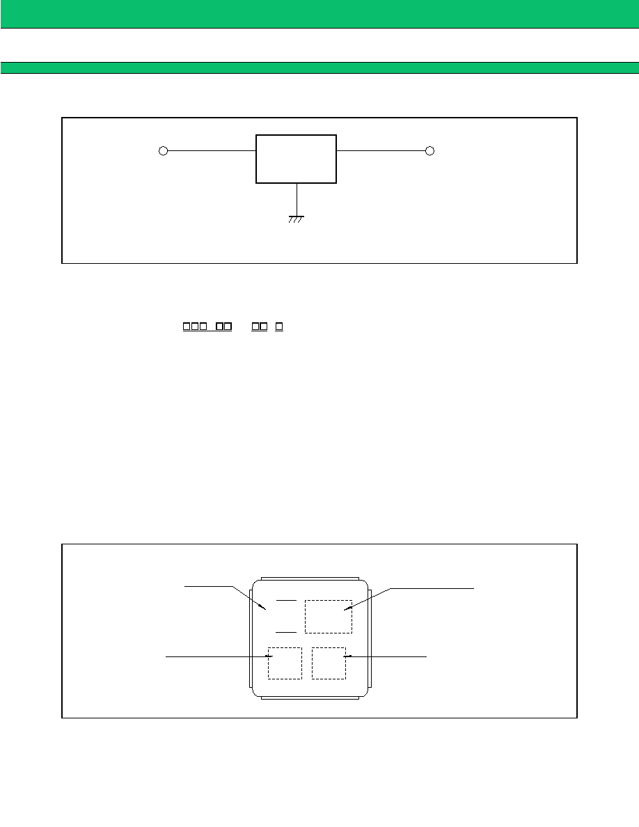
MEASURING CIRCUIT
s
PART NUMBER DESIGNATION
s
MARKING
1
2
3
6
5
4
1 to 6: Pin numbers
[Designation example]
(1) Frequency designation : Specify the nominal frequency in six alphanumeric characters.
Enter M (for MHz) at the decimal point.
Refer to standard frequencies.
[Example]
836.5 MHz
836M50
(2) Serial number
: Specify a characters from 01 to 99.
Refer to standard frequencies.
(3) Packing (Reeled tape) : W : 1 k pcs/reel
V : 3 k pcs/reel
U : 5 k pcs/reel
FAR≠F5CE≠
≠D2
≠
(1)
(2) (3)
M
F
B A
32
PART SYMBOL
LOGO
DATE CODE
LOT No.
16
F5CE Series (D2 type)
s
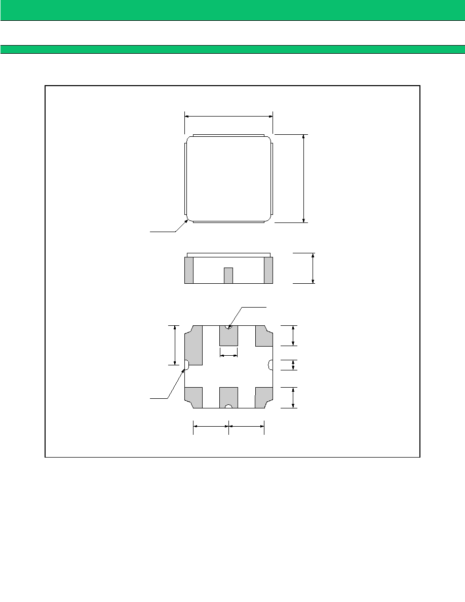
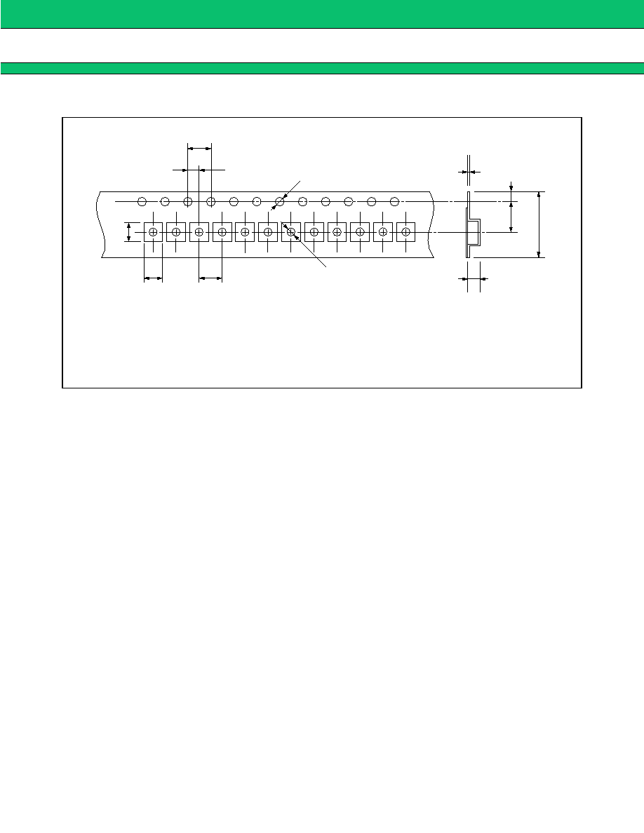
PACKAGE DIMENSION
* : Two types of package are available.
One of them may be supplied without these cut outs.
Dimensions in mm
3.0
3.0
1.2 MAX
0.75
0.75
4-R 0.3
1.2
0.6
1.5
1.2
*
2-R 0.2
0.4
1
2
3
6
5
4
17
F5CE Series (D2 type)
s
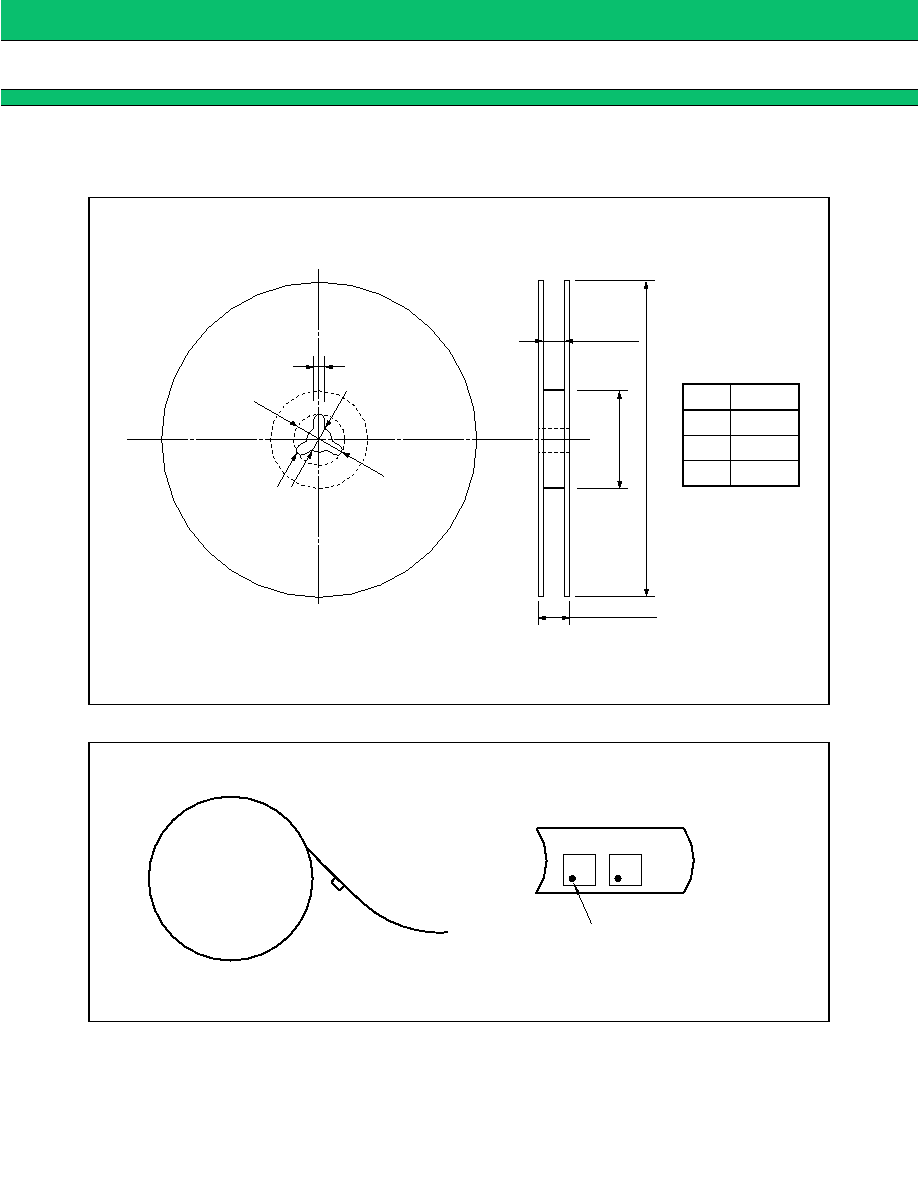
PACKING: Reel type
1. Reel Dimensions
2. Packing Style
Dimensions in mm
2 . 0
±
0 . 5
1 3 . 0
±
0 . 2
2 1 . 0
±
0 . 8
R 1 . 0
1 2 . 4
±
80
250
2.0
0.0
1
8.4 MAX
Type Volume
W
1 k pcs
V
3 k pcs
U
5 k pcs
# 1 P I N
F F
P u l l i n g s i d e
R e e l s i d e
P u l l i n g s i d e
18
F5CE Series (D2 type)
3. Tape Dimensions
Dimensions in mm
4 . 0
±
0 . 1
2 . 0
±
0 . 0 5
5.5
±
0.1
3.3
±
0.1
1 . 5
±
0.1
0
1 . 5
0 . 3
12.0
±
0.3
4 . 0
±
0 . 1
3 . 3
±
0 . 1
1.75
±
0.1
1 . 5

19
F5CE Series (D2 type)
FUJITSU LIMITED
For further information please contact:
Japan
FUJITSU LIMITED
Corporate Global Business Support Division
Electronic Devices
KAWASAKI PLANT, 4-1-1, Kamikodanaka
Nakahara-ku, Kawasaki-shi
Kanagawa 211-8588, Japan
Tel: (044) 754-3763
Fax: (044) 754-3329
http://www.fujitsu.co.jp/
North and South America
FUJITSU MICROELECTRONICS, INC.
Semiconductor Division
3545 North First Street
San Jose, CA 95134-1804, USA
Tel: (408) 922-9000
Fax: (408) 922-9179
Customer Response Center
Mon. - Fri.: 7 am - 5 pm (PST)
Tel: (800) 866-8608
Fax: (408) 922-9179
http://www.fujitsumicro.com/
Europe
FUJITSU MIKROELEKTRONIK GmbH
Am Siebenstein 6-10
D-63303 Dreieich-Buchschlag
Germany
Tel: (06103) 690-0
Fax: (06103) 690-122
http://www.fujitsu-ede.com/
Asia Pacific
FUJITSU MICROELECTRONICS ASIA PTE LTD
#05-08, 151 Lorong Chuan
New Tech Park
Singapore 556741
Tel: (65) 281-0770
Fax: (65) 281-0220
http://www.fmap.com.sg/
F9806
©
FUJITSU LIMITED Printed in Japan
All Rights Reserved.
The contents of this document are subject to change without
notice. Customers are advised to consult with FUJITSU sales
representatives before ordering.
The information and circuit diagrams in this document presented
as examples of semiconductor device applications, and are not
intended to be incorporated in devices for actual use. Also,
FUJITSU is unable to assume responsibility for infringement of
any patent rights or other rights of third parties arising from the
use of this information or circuit diagrams.
FUJITSU semiconductor devices are intended for use in
standard applications (computers, office automation and other
office equipment, industrial, communications, and measurement
equipment, personal or household devices, etc.).
CAUTION:
Customers considering the use of our products in special
applications where failure or abnormal operation may directly
affect human lives or cause physical injury or property damage,
or where extremely high levels of reliability are demanded (such
as aerospace systems, atomic energy controls, sea floor
repeaters, vehicle operating controls, medical devices for life
support, etc.) are requested to consult with FUJITSU sales
representatives before such use. The company will not be
responsible for damages arising from such use without prior
approval.
Any semiconductor devices have inherently a certain rate of
failure. You must protect against injury, damage or loss from
such failures by incorporating safety design measures into your
facility and equipment such as redundancy, fire protection, and
prevention of over-current levels and other abnormal operating
conditions.
If any products described in this document represent goods or
technologies subject to certain restrictions on export under the
Foreign Exchange and Foreign Trade Control Law of Japan, the
prior authorization by Japanese government should be required
for export of those products from Japan.