1
DS04-21709-1E
FUJITSU SEMICONDUCTOR
DATA SHEET
ASSP
Piezoelectric VCO
(4 to 30 MHz)
M2 Series (F100)
s
DESCRIPTION
The M2 series (F100) of VCO (Voltage Controlled Oscillator) apply to the frequency range 4-30 MHz.
The M2 series of VCO have a high reliability and wide controllable frequency ranges using a LiTaO
3
piezoelectric
single crystal with high electromechanical coupling coefficient. Output level applies to CMOS type for digital interface.
s
FEATURES
∑ Wide frequency controllable range (Over than ±2000 ppm)
∑ High carrier noise ratio
∑ Excellent temperature stability
∑ CMOS output level
∑ High reliability due to hermetic seal
s
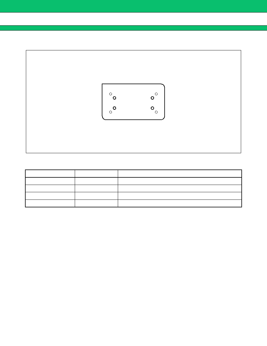
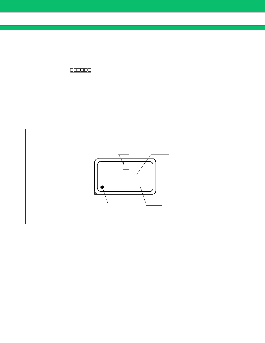
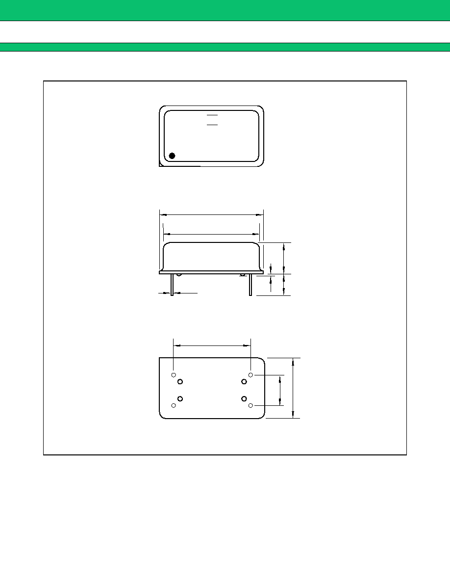
PACKAGE
F
14 pin DIP size, Metal can package
3
M2 Series (F100)
s
ABSOLUTE MAXIMUM RATINGS (See WARNING)
WARNING: Permanent device damage may occur if the above Absolute Maximum Ratings are exceeded.
Functional operation should be restricted to the conditions as detailed in the operational sections of
this data sheet. Exposure to absolute maximum rating conditions for extended periods may affect device
reliability.
s
RECOMMENDED OPERATING CONDITIONS
s
STANDARD FREQUENCIES
Parameter
Symbol
Rating
Unit
Power supply voltage
V
CC
≠0.5 to +7.0
V
Control voltage
V
IN
≠0.5 to +7.0
V
Operating temperature
T
a
≠10 to +70
∞
C
Storage temperature
T
stg
≠40 to +100
∞
C
Frequency range
--
+4 to +30
MHz
Parameter
Symbol
Value
Unit
Power supply voltage
V
CC
+4.75 to +5.25
V
Control voltage
V
IN
+0.0 to +5.0
V
Operating temperature
T
a
≠10 to +70
∞
C
Frequency
Application
Part number
12.288 MHz
For audio
FAR-M2DB-12M288-F100
13.500 MHz
For video
FAR-M2DB-13M500-F100
14.318 MHz
For video
FAR-M2DB-14M318-F100
18.432 MHz
For audio
FAR-M2DB-18M432-F100
21.053 MHz
For video
FAR-M2DB-21M053-F100
24.576 MHz
For audio
FAR-M2DB-24M576-F100
25.175 MHz
For video
FAR-M2DB-25M175-F100
27.000 MHz
For video
FAR-M2DB-27M000-F100
28.636 MHz
For video
FAR-M2DB-27M636-F100
5
M2 Series (F100)
s
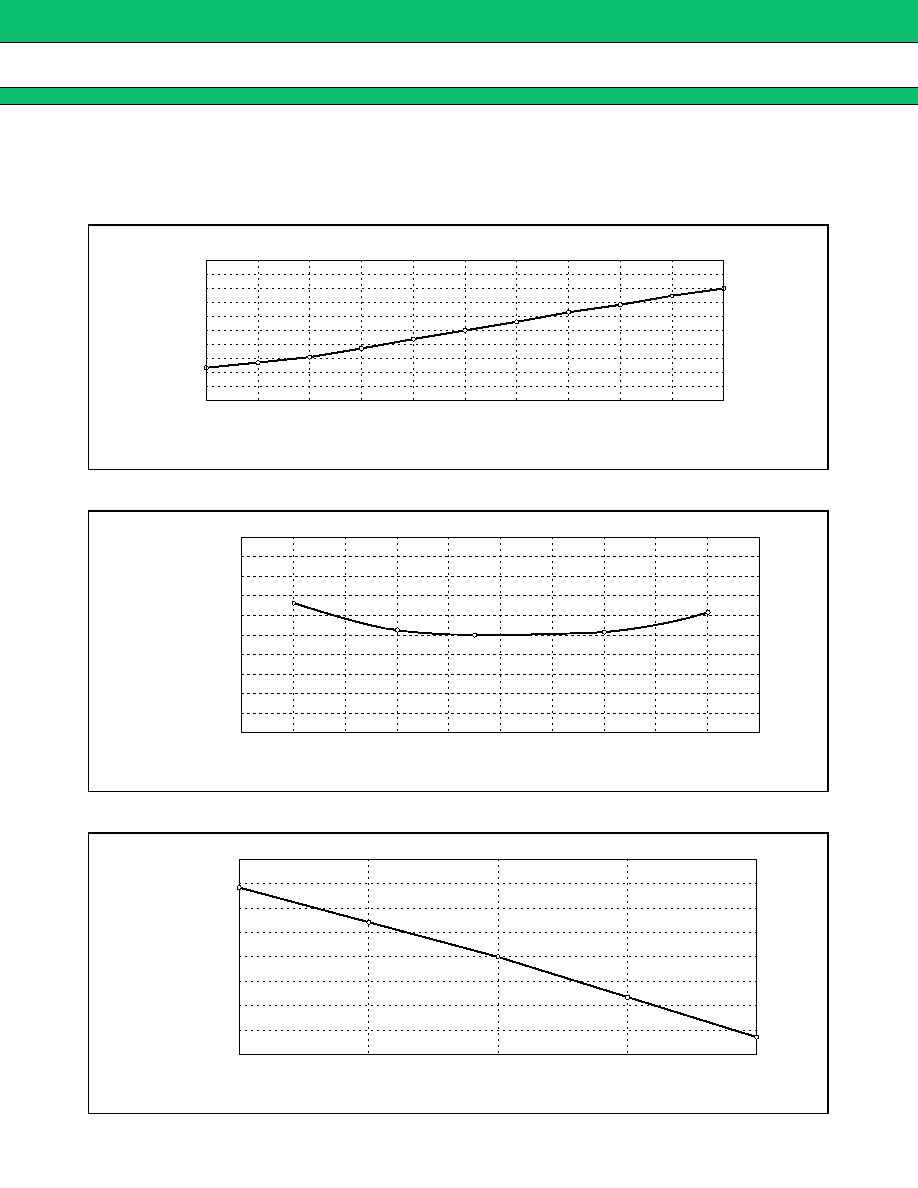
TYPICAL CHARACTERISTICS
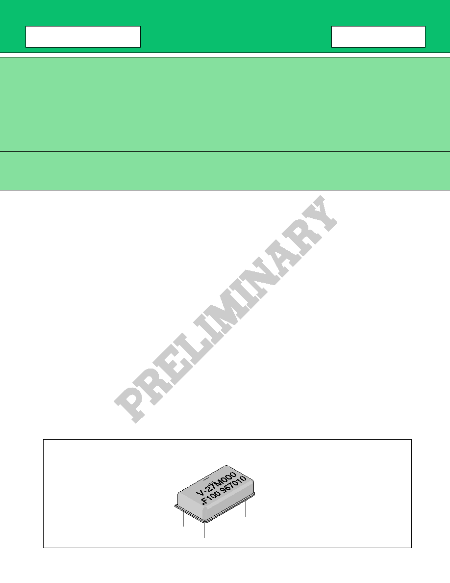
Part number : FAR-M2DB-27M000-F100
1. Oscillation Frequency vs. Control Votage
2. Frequency Stability With Temperature
(Ta = +25
∞
C reference)
3. Frequency Stability vs. Vcc
(V
CC
= +50
reference)
Oscillation Frequency (ppm)
Control Voltage (V)
5.000
4.000
3.000
2.000
1.000
0
-
1.000
-
2.000
-
3.000
-
4.000
-
5.000
0 0.5 1.0 1.5 2.0 2.5 3.0 3.5 4.0 4.5 5.0
27.000 MHz
Temperature (
∞
C)
Oscillation Frequency (ppm)
500
400
300
200
100
0
-
100
-
200
-
300
-
400
-
500
≠20 ≠10 0
10
20
30
40
50
60
70
80
V
IN
= +2.5 V
Vcc (V)
200
150
100
50
0
≠50
≠100
≠150
≠200
4.50
4.75
5.00
5.25
5.50
V
IN
= +2.5 V
Oscillation Frequency (ppm)

24
FUJITSU LIMITED
For further information please contact:
Japan
FUJITSU LIMITED
Corporate Global Business Support Division
Electronic Devices
KAWASAKI PLANT, 4-1-1, Kamikodanaka
Nakahara-ku, Kawasaki-shi
Kanagawa 211-88, Japan
Tel: (044) 754-3763
Fax: (044) 754-3329
North and South America
FUJITSU MICROELECTRONICS, INC.
Semiconductor Division
3545 North First Street
San Jose, CA 95134-1804, U.S.A.
Tel: (408) 922-9000
Fax: (408) 432-9044/9045
Europe
FUJITSU MIKROELEKTRONIK GmbH
Am Siebenstein 6-10
63303 Dreieich-Buchschlag
Germany
Tel: (06103) 690-0
Fax: (06103) 690-122
Asia Pacific
FUJITSU MICROELECTRONICS ASIA PTE. LIMITED
#05-08, 151 Lorong Chuan
New Tech Park
Singapore 556741
Tel: (65) 281-0770
Fax: (65) 281-0220
F9703
©
FUJITSU LIMITED Printed in Japan
All Rights Reserved.
The contents of this document are subject to change without
notice. Customers are advised to consult with FUJITSU sales
representatives before ordering.
The information and circuit diagrams in this document presented
as examples of semiconductor device applications, and are not
intended to be incorporated in devices for actual use. Also,
FUJITSU is unable to assume responsibility for infringement of
any patent rights or other rights of third parties arising from the
use of this information or circuit diagrams.
FUJITSU semiconductor devices are intended for use in
standard applications (computers, office automation and other
office equipment, industrial, communications, and measurement
equipment, personal or household devices, etc.).
CAUTION:
Customers considering the use of our products in special
applications where failure or abnormal operation may directly
affect human lives or cause physical injury or property damage,
or where extremely high levels of reliability are demanded (such
as aerospace systems, atomic energy controls, sea floor
repeaters, vehicle operating controls, medical devices for life
support, etc.) are requested to consult with FUJITSU sales
representatives before such use. The company will not be
responsible for damages arising from such use without prior
approval.
Any semiconductor devices have inherently a certain rate of
failure. You must protect against injury, damage or loss from
such failures by incorporating safety design measures into your
facility and equipment such as redundancy, fire protection, and
prevention of over-current levels and other abnormal operating
conditions.
If any products described in this document represent goods or
technologies subject to certain restrictions on export under the
Foreign Exchange and Foreign Trade Control Law of Japan, the
prior authorization by Japanese government should be required
for export of those products from Japan.