1
DS04-21703-3E
FUJITSU SEMICONDUCTOR
DATA SHEET
ASSP
Piezo Electric VCO
M2 Series (D110)
VOLTAGE CONTROLLED OSCILLATOR (4 to 30 MHz)
s
DESCRIPTION
The M2 series (D110) Voltage Controlled Oscillators (VCO) directly oscillate in the frequency range of 4 to 30 MHz.
The M2 series VCO use a piezoelectric single crystal with high electromechanical coupling coefficient (LiTaO3: lithium
tantalate) for stable and wide variable frequency width.
Excellent S/N and jitter characteristic due to high Q of lithium tantalate can realize high quality playback sound and
picture, especially in PLL circuit of digital audio and video equipments.
s
FEATURES
∑ Wider variable frequency width than quarts crystals:
±
0.2% or more
∑ High stability (100 times more stable than LC or TTL-IC VCO)
∑ Excellent S/N and jitter characteristic due to high Q of lithium tantalate for high quality playback sound and
picture.
∑ Excellent temperature characteristic: ≠300 ~ 500 ppm (≠10 ~ +70
∞
C)
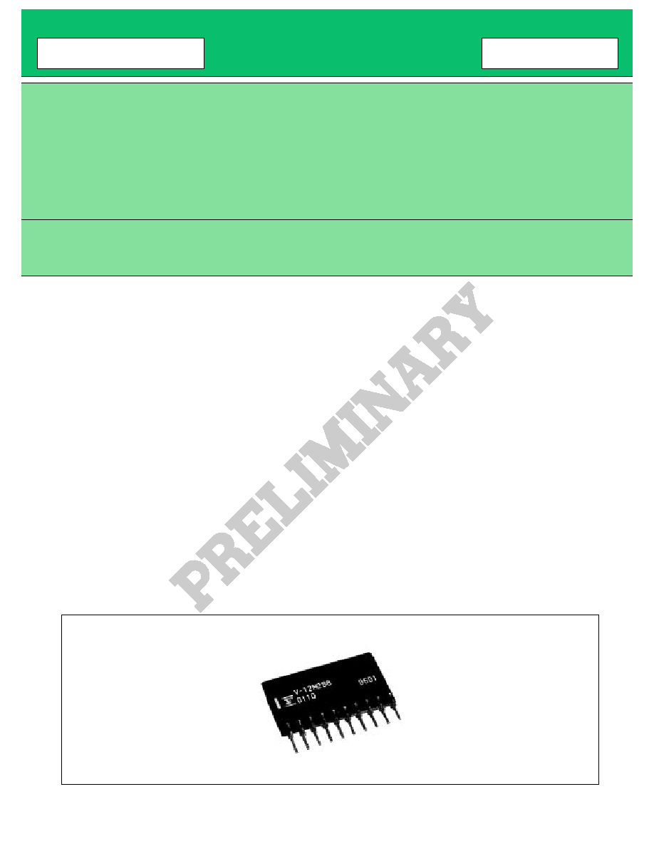
∑ 10-pin SIP ready for high-density mounting.
s
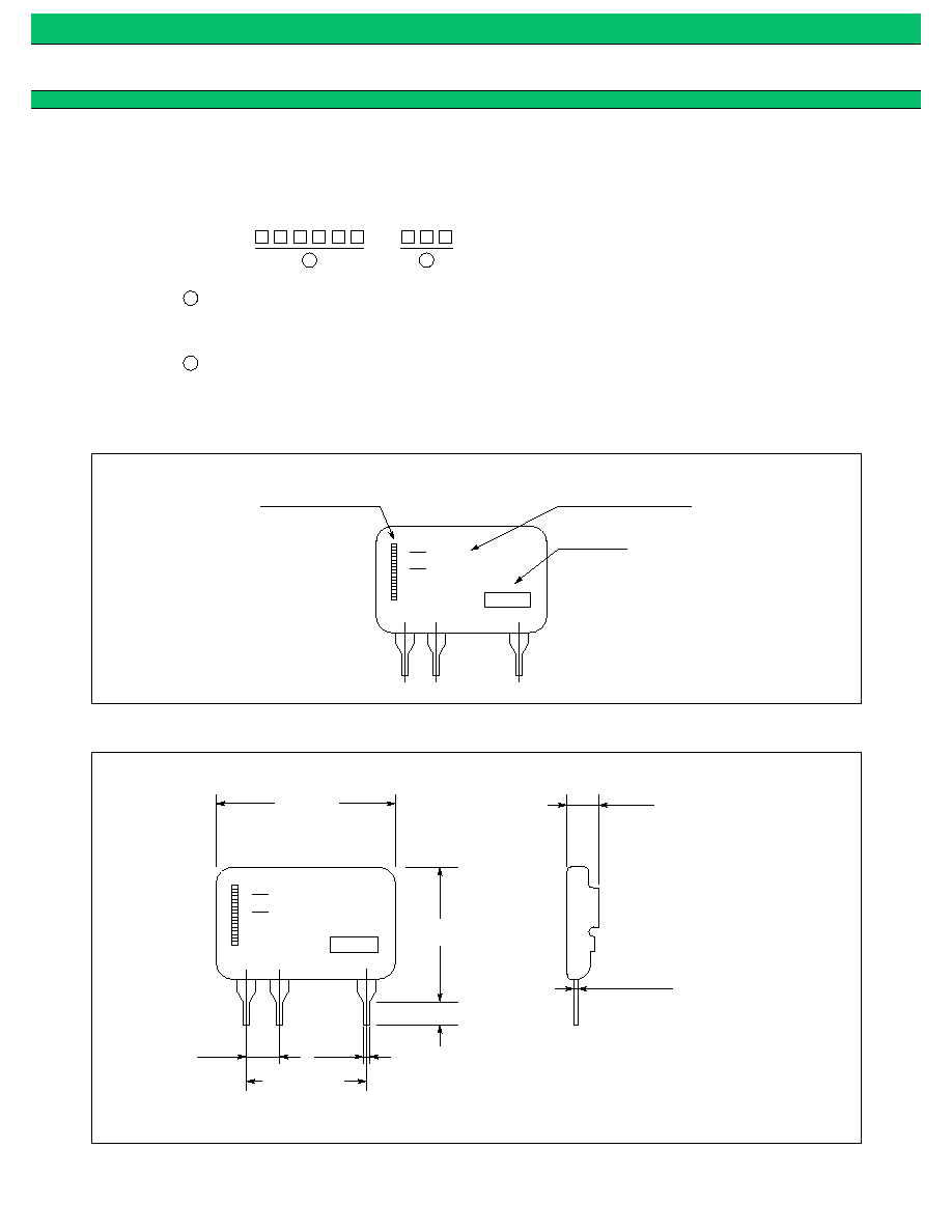
PACKAGE

2
M2 Series (D110)
s
TERMINAL ASSIGNMENT
s
MAXIMUM RATINGS
s
RECOMMENDED OPERATING CONDITIONS
s
STANDARD FREQUENCIES
Item
Symbol
Rated value
Unit
Power supply voltage
V
CC
≠0.5 ~ +7.0
V
Input control voltage
V
IN
≠0.5 ~ +10.0
Power consumption
P
D
100
mW
Operating temperature
Ta
≠10 ~ +70
∞
C
Storage temperature
Tstg
≠30 ~ +100
Oscillation frequency range
--
4 ~ 30
MHz
Item
Symbol
Rated value
Unit
Power supply voltage
V
CC
4.75 ~ 5.25
V
Input control voltage
V
IN
0 ~ 5
Operating temperature
Ta
≠10 ~ +60
∞
C
Frequencies
Uses
Part number
Frequencies
Uses
Part number
12.288 MHz
Audio
FAR-M2SC-12M288-D110
17.734 MHz
Video
FAR-M2SC-17M734-D110
13.500 MHz
Video
FAR-M2SC-13M500-D110
22.579 MHz
Audio
FAR-M2SC-22M579-D110
14.318 MHz
Video
FAR-M2SC-14M318-D110
24.576 MHz
Audio
FAR-M2SC-24M576-D110
16.934 MHz
Audio
FAR-M2SC-16M934-D110
28.636 MHz
Video
FAR-M2SC-28M636-D110
Note: The GND terminals are not connected inside the module.
Be sure to route them on the PC board.
Terminal No.
Terminal Name
Description
1
V
IN
Control voltage input terminal
2, 3, 4, 5, 6, 7
A-GND
Analog grounding terminal
8
V
OUT
Output terminal
9
V
CC
Power supply terminal
10
D-GND
Digital grounding terminal
(Front view)
10
9
8
7
6
5
4
3
2
1
D-GND
V
CC
V
OUT
A-GND
A-GND
A-GND
A-GND
A-GND
A-GND
V
IN
3
M2 Series (D110)
s
ELECTRICAL CHARACTERISTICS
(V
CC
= 5.0 V)
*1: V
CC
= 5.0 V standard
*2: 25
∞
C standard, Ta = ≠10 ~ +70
∞
C
s
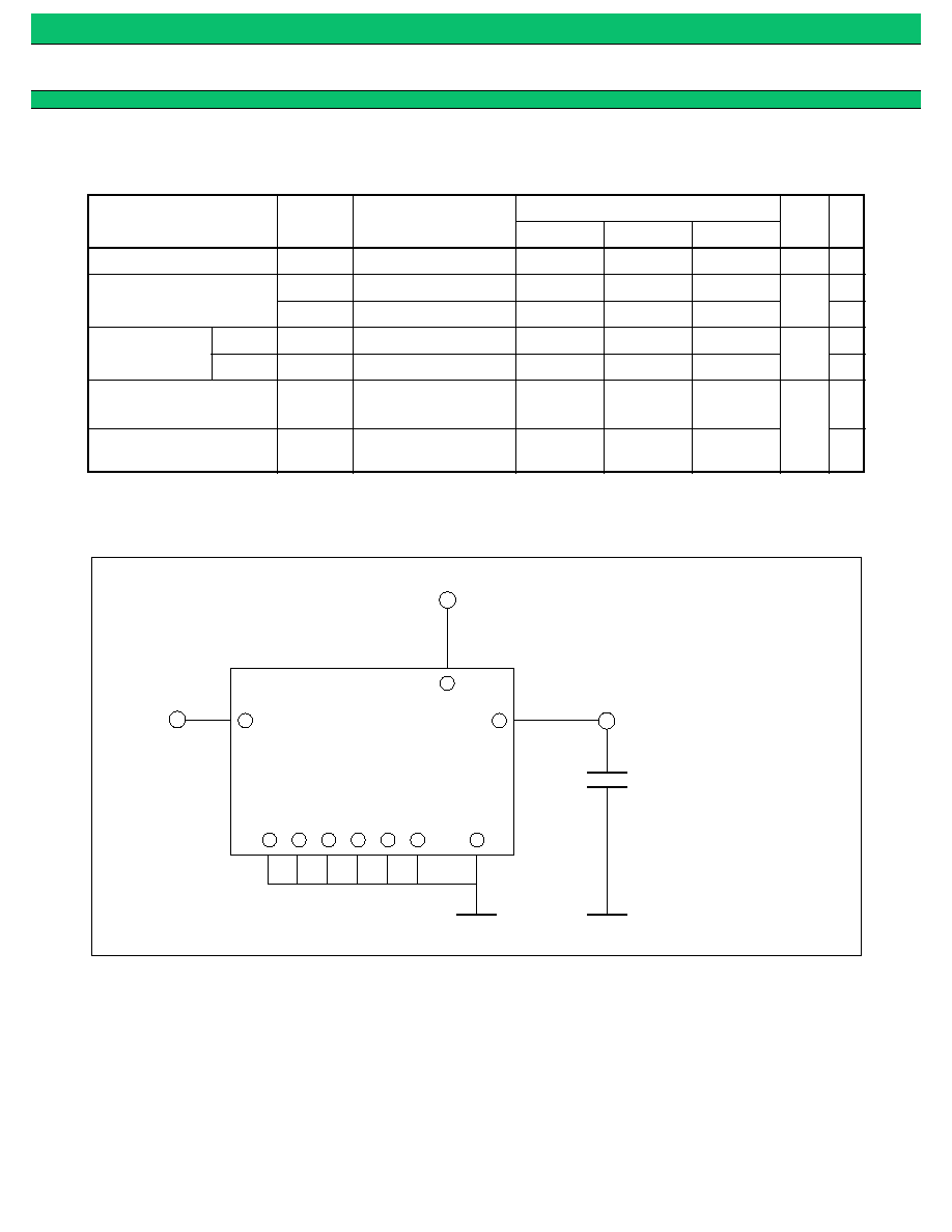
MEASURING CIRCUIT DIAGRAM
Item
Symbol
Condition
Rated value
Unit
minimum
standard
maximum
Power supply current
I
CC
Not loaded
--
10
15
mA
Oscillation frequency
f
H
V
IN
= 5.0 V
+2000
--
--
ppm
f
1
V
IN
= 0 V
--
--
≠2000
Output voltage
H level
V
OH
V
IN
= 2.5 V
V
CC
≠ 0.5
5.0
--
V
L level
V
OL
V
IN
= 2.5 V
--
0
0.5
Frequency voltage
stability
f (V
CC
)
V
CC
= 4.75 ~ 5.25 V
≠100
--
+100
ppm
*1
Frequency temperature
stability
f (Ta)
V
IN
= 2.5 V
≠300
--
+500
*2
1
3
4
5
6
7
9
10
8
V
CC
V
IN
Into oscilloscope
Including probe
capacity (22 pF)
GND
2

24
FUJITSU LIMITED
For further information please contact:
Japan
FUJITSU LIMITED
Corporate Global Business Support Division
Electronic Devices
KAWASAKI PLANT, 4-1-1, Kamikodanaka
Nakahara-ku, Kawasaki-shi
Kanagawa 211-88, Japan
Tel: (044) 754-3763
Fax: (044) 754-3329
North and South America
FUJITSU MICROELECTRONICS, INC.
Semiconductor Division
3545 North First Street
San Jose, CA 95134-1804, U.S.A.
Tel: (408) 922-9000
Fax: (408) 432-9044/9045
Europe
FUJITSU MIKROELEKTRONIK GmbH
Am Siebenstein 6-10
63303 Dreieich-Buchschlag
Germany
Tel: (06103) 690-0
Fax: (06103) 690-122
Asia Pacific
FUJITSU MICROELECTRONICS ASIA PTE. LIMITED
#05-08, 151 Lorong Chuan
New Tech Park
Singapore 556741
Tel: (65) 281-0770
Fax: (65) 281-0220
F9703
©
FUJITSU LIMITED Printed in Japan
All Rights Reserved.
The contents of this document are subject to change without
notice. Customers are advised to consult with FUJITSU sales
representatives before ordering.
The information and circuit diagrams in this document presented
as examples of semiconductor device applications, and are not
intended to be incorporated in devices for actual use. Also,
FUJITSU is unable to assume responsibility for infringement of
any patent rights or other rights of third parties arising from the
use of this information or circuit diagrams.
FUJITSU semiconductor devices are intended for use in
standard applications (computers, office automation and other
office equipment, industrial, communications, and measurement
equipment, personal or household devices, etc.).
CAUTION:
Customers considering the use of our products in special
applications where failure or abnormal operation may directly
affect human lives or cause physical injury or property damage,
or where extremely high levels of reliability are demanded (such
as aerospace systems, atomic energy controls, sea floor
repeaters, vehicle operating controls, medical devices for life
support, etc.) are requested to consult with FUJITSU sales
representatives before such use. The company will not be
responsible for damages arising from such use without prior
approval.
Any semiconductor devices have inherently a certain rate of
failure. You must protect against injury, damage or loss from
such failures by incorporating safety design measures into your
facility and equipment such as redundancy, fire protection, and
prevention of over-current levels and other abnormal operating
conditions.
If any products described in this document represent goods or
technologies subject to certain restrictions on export under the
Foreign Exchange and Foreign Trade Control Law of Japan, the
prior authorization by Japanese government should be required
for export of those products from Japan.