 | –≠–ª–µ–∫—Ç—Ä–æ–Ω–Ω—ã–π –∫–æ–º–ø–æ–Ω–µ–Ω—Ç: FHR02X | –°–∫–∞—á–∞—Ç—å:  PDF PDF  ZIP ZIP |
1
Edition 1.3
September 1999
FHR02X
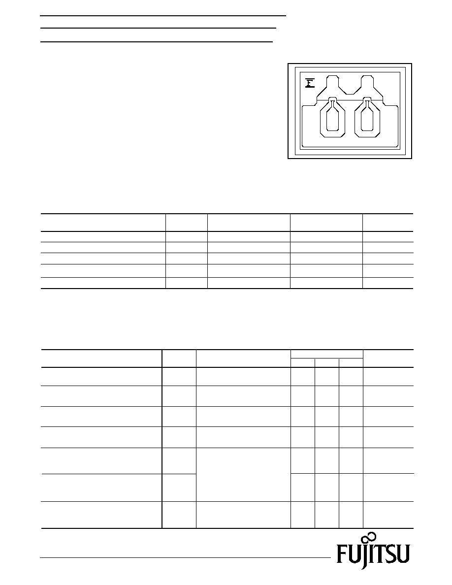
GaAs FET & HEMT Chips
Item
Saturated Drain Current
Transconductance
Pinch-off Voltage
Gate Source Breakdown Voltage
Noise Figure
Associated Gain
Symbol
IDSS
15
30
60
35
45
-
-0.2
-0.7
-1.5
-3.0
-
-
8
9
-
-
1.0
1.2
VDS = 2V, IDS = 1mA
VDS = 2V, IDS = 10mA
VDS = 2V, VGS = 0V
IGS = -10µA
VDS = 2V
IDS = 10mA
f = 18GHz
mA
mS
V
dB
dB
V
gm
Vp
VGSO
NF
Gas
Test Conditions
Unit
Limit
Typ.
Max.
Min.
ELECTRICAL CHARACTERISTICS (Ambient Temperature Ta=25∞C)
Note: RF parameter sample size 10pcs. criteria (accept/reject)=(2/3)
Channel to Case
-
220
300
∞C/W
Thermal Resistance
Rth
The chip must be enclosed in a hermetically sealed environment for optimum performance and reliability.
Item
Drain-Source Voltage
Gate-Source Voltage
Total Power Dissipation
Storage Temperature
Channel Temperature
Symbol
VDS
VGS
3.5
-3.0
180
-65 to +175
175
Note
V
V
mW
∞C
∞C
Ptot
Tstg
Tch
Condition
Unit
Rating
ABSOLUTE MAXIMUM RATING (Ambient Temperature Ta=25∞C)
Note: Mounted on Al2O3 board (30 x 30 x 0.65mm)
Fujitsu recommends the following conditions for the reliable operation of GaAs FETs:
1. The drain-source operating voltage (VDS) should not exceed 2 volts.
2. The forward and reverse gate currents should not exceed 0.2 and -0.05 mA respectively with
gate resistance of 4000.
3. The operating channel temperature (Tch) should not exceed 80∞C.
FEATURES
∑ Low Noise Figure: 1.0dB (Typ.)@f=18GHz
∑ High Associated Gain: 9.0dB (Typ.)@f=18GHz
∑ Lg 0.25µm, Wg = 200µm
∑ Gold Gate Metallization for High Reliability
DESCRIPTION
The FHX02X is a High Electron Mobility Transistor(HEMT)
intended for general purpose, ultra-low noise and high gain
amplifiers in the 4-22GHz frequency range. This device is well
suited for telecommunication, radio link or other low noise
applications.
Fujitsu's stringent Quality Assurance Program assures the highest
reliability and consistent performance.
2
FHR02X
GaAs FET & HEMT Chips
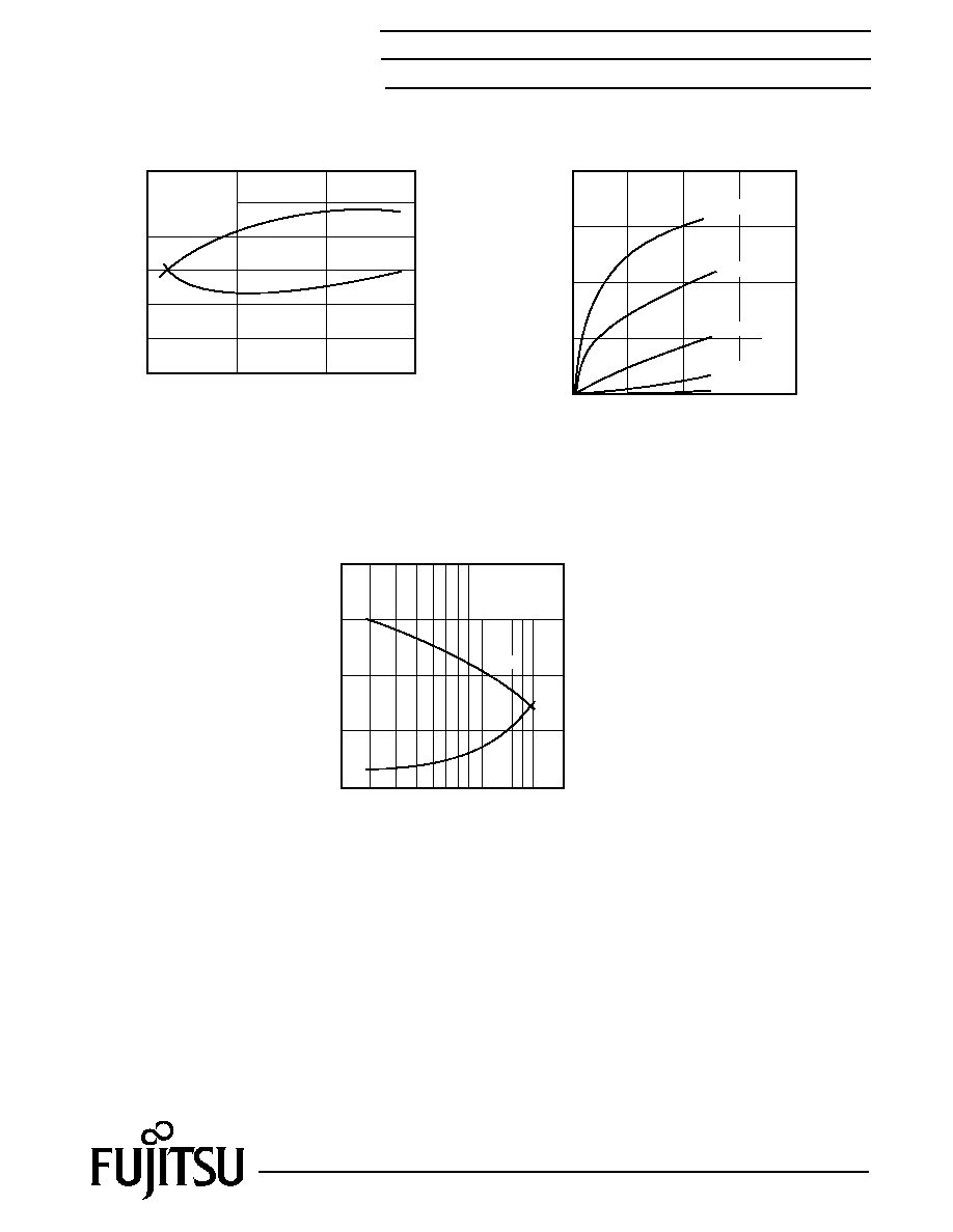
NF & Gas vs. IDS
NF & Gas vs. Frequency
DRAIN CURRENT vs. DRAIN-SOURCE VOLTAGE
3
f=18GHz
VDS=2V
VDS=2V
IDS=10mA
Gas
Gas
NF
NF
2
1
0
11
10
9
8
7
6
10
20
30
4
6
8 1012
20
1
2
3
4
Drain Current (mA)
Frequency (GHz)
Drain-Source Voltage (V)
Noise Figure (dB)
40
30
0
10
20
2
3
4
1
0
10
15
20
5
0
Drain Current (mA)
Noise Figure (dB)
Associated Gain (dB)
Associated Gain (dB)
Vgs =0V
-0.2V
-0.4V
-0.6V
-0.8V
3
FHR02X
GaAs FET & HEMT Chips
NOISE PARAMETERS
VDS=2V, IDS=10mA
Freq.
(GHz)
opt
(MAG) (ANG)
NFmin
(dB)
Rn/50
2
4
6
8
10
12
14
16
18
20
22
24
26
28
30
0.80
0.74
0.68
0.63
0.58
0.52
0.47
0.42
0.38
0.33
0.30
0.28
0.26
0.25
0.24
16
31
46
61
75
89
102
114
126
137
146
155
162
171
-170
0.33
0.35
0.44
0.53
0.63
0.70
0.81
0.92
1.04
1.16
1.34
1.56
1.78
2.00
2.34
0.50
0.45
0.40
0.30
0.23
0.18
0.14
0.12
0.10
0.09
0.09
0.09
0.08
0.08
0.08
S-PARAMETERS
VDS = 2V, IDS = 10mA
FREQUENCY
S11
S21
S12
S22
(MHZ)
MAG
ANG
MAG
ANG
MAG
ANG
MAG
ANG
100
1.000
-1.0
4.073
179.2
.001
89.5
.607
-0.4
500
.999
-4.8
4.068
175.9
.007
87.7
.607
-2.2
1000
.995
-9.6
4.054
171.9
.013
85.4
.605
-4.3
2000
.982
-19.1
3.999
163.9
.026
80.9
.599
-8.6
4000
.934
-37.4
3.801
148.5
.049
72.7
.576
-16.5
6000
.868
-54.5
3.530
134.5
.068
65.9
.544
-23.5
8000
.799
-70.3
3.237
121.9
.082
60.9
.511
-29.5
10000
.734
-84.9
2.955
110.8
.093
57.5
.479
-34.8
12000
.678
-98.4
2.700
100.8
.101
55.6
.450
-39.6
14000
.633
-111.2
2.476
91.7
.108
55.0
.424
-44.1
16000
.597
-123.1
2.282
83.5
.115
55.4
.402
-48.6
18000
.571
-134.5
2.114
75.9
.122
56.6
.382
-53.3
20000
.553
-145.2
1.969
68.9
.131
58.1
.364
-58.4
22000
.543
-155.2
1.842
62.3
.141
59.6
.348
-63.9
24000
.539
-164.7
1.731
56.0
.154
61.0
.334
-70.0
26000
.540
-173.5
1.633
50.1
.168
62.0
.320
-76.9
28000
.545
178.2
1.544
44.5
.185
62.5
.309
-84.5
30000
.554
170.5
1.465
39.1
.203
62.4
.300
-93.0
NOTE:*
The data includes bonding wires.
n: number of wires
Gate
n=2 (0.2mm length, 25µm Dia Au wire)
Drain n=2 (0.2mm length, 25µm Dia Au wire)
Source n=4 (0.3mm length, 25µm Dia Au wire)
Download S-Parameters, click here
For further information please contact:
FUJITSU COMPOUND SEMICONDUCTOR, INC.
2355 Zanker Rd.
San Jose, CA 95131-1138, U.S.A.
Phone: (408) 232-9500
FAX: (408) 428-9111
www.fcsi.fujitsu.com
FUJITSU MICROELECTRONICS, LTD.
Compound Semiconductor Division
Network House
Norreys Drive
Maidenhead, Berkshire SL6 4FJ
Phone:+44 (0)1628 504800
FAX:+44 (0)1628 504888
Fujitsu Limited reserves the right to change products and specifications without notice.
The information does not convey any license under rights of Fujitsu Limited or others.
© 1998 FUJITSU COMPOUND SEMICONDUCTOR, INC.
Printed in U.S.A. FCSI0598M200
Fujitsu Compound Semiconductor Products contain gallium arsenide
(GaAs) which can be hazardous to the human body and the environment.
For safety, observe the following procedures:
CAUTION
∑ Do not put these products into the mouth.
∑ Do not alter the form of this product into a gas, powder, or liquid
through burning, crushing, or chemical processing as these by-products
are dangerous to the human body if inhaled, ingested, or swallowed.
∑ Observe government laws and company regulations when discarding this
product. This product must be discarded in accordance with methods
specified by applicable hazardous waste procedures.
4
FHR02X
GaAs FET & HEMT Chips
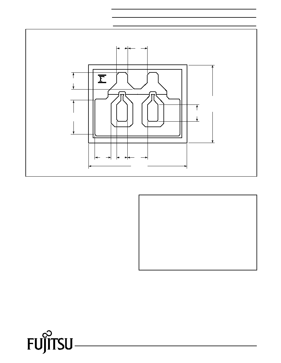
CHIP OUTLINE
(Unit: µm)
90
75
90
450±20
154
350
±
20
75
75
50
50
Die Thickness:
100±20µm