 | –≠–ª–µ–∫—Ç—Ä–æ–Ω–Ω—ã–π –∫–æ–º–ø–æ–Ω–µ–Ω—Ç: FIM83010 | –°–∫–∞—á–∞—Ç—å:  PDF PDF  ZIP ZIP |

FEATURES
∑ 300-pin MSA compliant
∑ SONET OC-192, SDH STM-64, 10G Ethernet and FEC rate compliant
(9.953Gbps/10.313Gbps/10.71Gbps)
∑ Tunable wavelength locker LD module can select one wavelength
from four wavelengths with 100GHz space as specified
in ITU-T grid
∑ Tunable wavelength locker LD module, Lithium Niobate (LiNbO3)
modulator and APD
∑ 16:1 MUX and 1:16 DEMUX integrated with OIF-SFI4-P1
compliant interface
∑ Compact size (4.5"L x 3.5"W x 0.53"H)
DESCRIPTION
Fujitsu has developed a product line of serial 10Gbps transponders that incorporate all of the features
required by the 300-pin Multi-Source Agreement and Optical Internetworking Forum (OIF-SFI4_01.0)
specification.
The FIM83010 is a 4 ITU-T channel tunable 10Gbps Dense Wavelength Multiplexing (DWDM) Optical
Transponder that focuses on Metro network and Long Haul applications. Modules are available to cover
all wavelengths in the C band. The transponder includes a Tunable wavelength locker LD,
Lithium Niobate modulator and APD with a 16 bit parallel electrical interface. The Fujitsu FIM83010
can be operated at any one of three different data rates, 9.953Gbps(SONET OC-192)/10.313Gbps
(Ethernet IEEE802.3ae)/10.709Gbps(ITU-T G.709).
1
Edition 1.0
January 2003
10Gb/s Optical Transponder
for DWDM
FIM83010
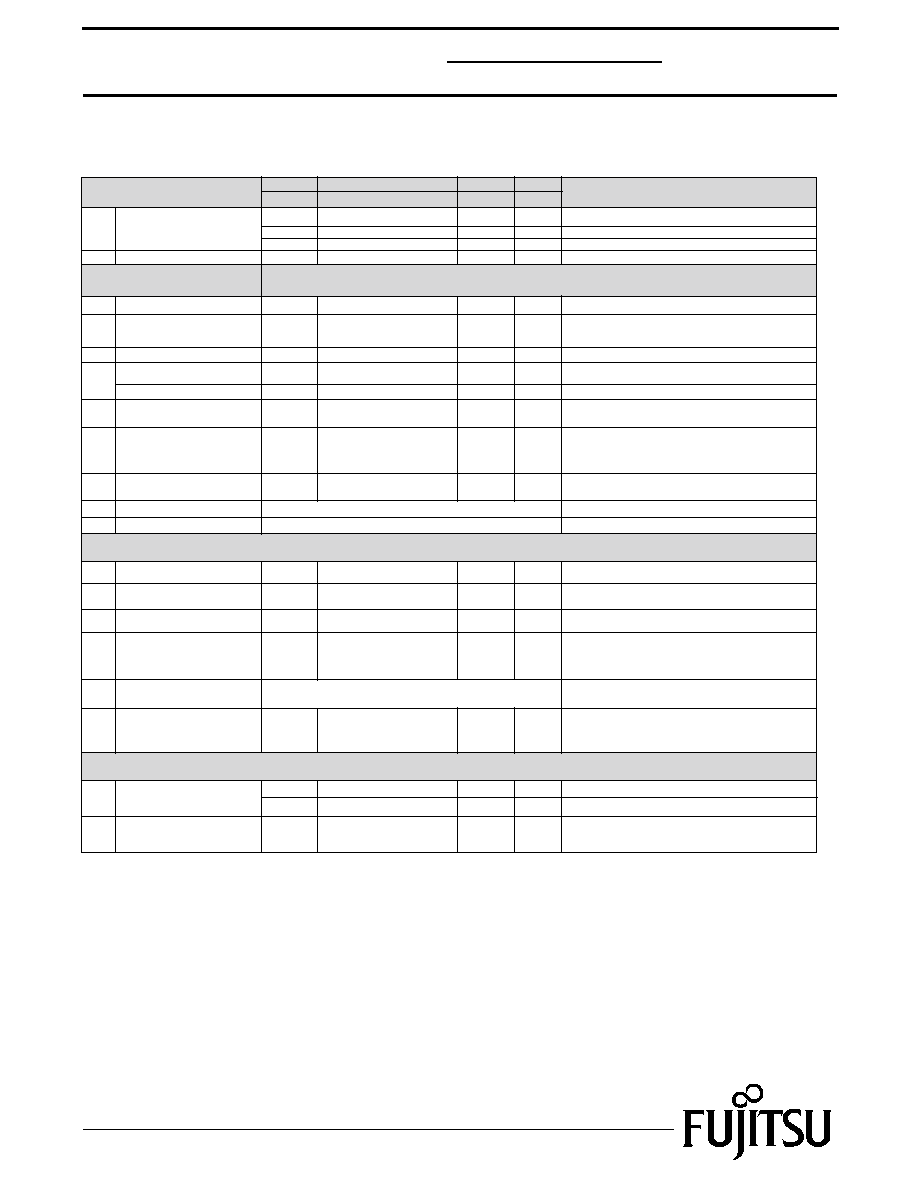
Parameter
Symbol
Supply Voltage
Remarks
See Fig. 1
Storage Humidity
%
Unit
ABSOLUTE MAXIMUM RATINGS (Tc=25
∞C, Unless otherwise specified)
Limits
Typ.
Max.
Storage Temperature
Tstg
∞C
-
85
-40
Optical Input Power
Pin
Peak Power
dBm
-
+3
-
LVDS Input Voltage
ILVDS-in
V
-
2.7
0
LVDS Output Voltage
ILVDS-out
V
-
2.0
0
Electrostatic Discharge
ESD
Human Body Model
V
-
500
-
VCC
+5.0V
V
-
+6.0
0.0
VDD1
+3.3V
V
-
+3.6
-0.3
VDD2
+1.8V
V
-
+2.0
-0.5
VEE
-5.2V
V
-
0.0
-6.0
TTL Input Voltage
VTTL-in
V
-
3.6
0
Min.
Menu
Description
Data Rate
1
9.953Gbps
SONET OC-192/SDH STM-64
2
10.313Gbps
10GBE (IEEE802.3ae)
3
10.709Gbps
ITU-T G.709
MENU

2
10Gb/s Optical Transponder
for DWDM
FIM83010
RECOMMENDED OPERATING CONDITIONS
Parameter
Symbol
Supply Current
Supply Voltage
Remarks
Unit
Limits
Typ.
Max.
Case Temperature
Tc
∞C
-
70
-5
Operating Humidity
See Fig. 2
%
Power Dissipation
Pd
W
8.5
12.0
-
VCC
5.0
5.25
4.75
VDD1
V
V
3.3
3.47
3.13
VDD2
V
1.8
1.89
1.71
VEE
V
-5.2
-4.94
-5.46
ICC
150
700
-
Min.
mA
mA
IDD1
350
500
-
mA
IDD2
920
1200
-
mA
IEE
950
1900
-
∑ Typical condition: Ta=Room Temp.
∑ Maximum condition: Tc=-5 or 70
∞C
∑ Under power supply startup
Fig. 1 Storage Humidity Criteria vs. Ambient Temperature
Ambient Temperature (
∞C)
Humidity (%)
30%
40%
50%
60%
70%
Constant Humidity
Ratio of 0.024kg Water/Kg Dry Air
80%
20%
10%
0%
90%
100%
-10
70
60
50
40
-40
30
-30
20
-20
80
0
10
90
Safe Storage Area
Fig. 2 Operating Humidity Criteria vs. Ambient Temperature
Ambient Temperature (
∞C)
Humidity (%)
30%
40%
50%
60%
70%
Constant Humidity
Ratio of 0.024kg Water/Kg Dry Air
80%
20%
10%
0%
90%
100%
-10
70
60
50
40
30
20
80
0
10
90
Safe Operating Area

3
Jitter
Filter
Mux
CDR/
Dem
ux
TEC Con
troller
Contr
ol
LN
Modulator
Driver
Amp
LIM-
Amp
CW La
ser
With Loc
ker
EEPR
OM
OPT
in
OPT
out
APD
/Pre
MOD
RxRA
TESEL(0:1)
RxMUTEP
OCLK
RxM
UTE
MCLK
RxM
UTE
DOUT
RxLCKREF
RxLSBSEL
RxREFSEL
RxLOCKER
R
RxDTV
I2CC
LOCK
IC2D
ATA
I2CAD(0:
2)
LsPO
WMON
LsBIASMON
LsP
OW
ALM
LsBIASALM
LsW
AVELOCKALM
RxP
OWMON
RxP
OW
ALM
TxTRA
CE
TxDin(15:0)
TxPICLK(P/N)
TxPCLK(
P/N)
TxM
CLK(P/N)
RxLCKREF
RxREFSEL
RxREFCLK(P/N)
RxMCLK(P/N)
TxLOCKER
R
TxREFCLK(P/N)
TxFIFORES
TxFIFOER
R
RxDOUT(15:0)
RxP
OCLK(
P/N)
TxREFSEL
TxRA
TESEL(0/1)
TxLSBSEL
LsENABLE
LsTUNE(0:
2)
TxRESE
T
TxCHIRPSEL
10Gb/s Optical Transponder
for DWDM
FIM83010
Optical Transponder Block Diagram
SYSTEM APPLICATION
Parameter
Specifications
Optical Connector
SC-Advanced PC, LC-Advanced PC
Data Rate
9.953Gbps, 10.313Gbps, 10.709Gbps
Operating Wavelength Range
1528.77 ~ 1566.31nm
Tx
1290 ~ 1608nm
Rx
Transmission Distance
80km

4
10Gb/s Optical Transponder
for DWDM
FIM83010
VCC
FFU
GND RxDout12P
VDD2
RxDout8P
GND
RxDout4P
GND
RxDout0P
K J
H G
F
E
D
C
B
A
VCC
FFU
GND RxDout12N
VDD2
RxDout8N
GND
RxDout4N
GND
RxDout0N
VDD1
NUC
GND RxDout13P
VDD1
RxDout9P
GND
RxDout5P
GND
RxDout1P
VDD1
NUC
GND RxDout13N
VDD1
RxDout9N
GND
RxDout5N
GND
RxDout1N
VDD1
FFU
GND TxDin13P
VDD1
TxDin9P
GND
TxDin5P
GND
TxDin1P
VDD1
FFU
GND TxDin13N
VDD1
TxDin9N
GND
TxDin5N
GND
TxDin1N
VDD1
FFU
GND RxDout14P
VDD1
RxDout10P
GND
RxDout6P
GND
RxDout2P
VDD1
RxLSBSEL
GND RxDout14N
VDD1
RxDout10N
GND
RxDout6N
GND
RxDout2N
VDD1
TxCHIRPSEL
GND TxDin14P
VDD1
TxDin10P
GND
TxDin6P
GND
TxDin2P
VDD1
TxLSBSEL
GND TxDin14N
VDD1
TxDin10N
GND
TxDin6N
GND
TxDin2N
VEE
FFU
GND RxDout15P
VEE
RxDout11P
GND
RxDout7P
GND
RxDout3P
VEE
FFU
GND RxDout15N
VEE
RxDout11N
GND
RxDout7N
GND
RxDout3N
VEE
FFU
GND TxPICLKP
VEE
TxPCLKP
GND
TxMCLKP
GND
TxREFCLKP
VEE
TxTRACE
GND TxPICLKN
VEE
TxPCLKN
GND
TxMCLKN
GND
TxREFCLKN
Receiver Power & GND supplies
Receiver DC Signals
Transmitter Power & GND Supplies
Transmitter DC signals
NUC: No User Connection
FFU: Reserved for Future Use
622 differential signals
VEE
NUC
GND TxDin15P
VEE
TxDin11P
GND
TxDin7P
GND
TxDin3P
VEE
NUC
GND TxDin15N
VEE
TxDin11N
GND
TxDin7N
GND
TxDin3N
VCC
FFU
GND TxDin12P
VDD2
TxDin8P
GND
TxDin4P
GND
TxDin0P
VCC
FFU
GND TxDin12N
VDD2
TxDin8N
GND
TxDin4N
GND
TxDin0N
VEE
FFU
GND FFU
VEE
RxPOCLKP
GND
RxMCLKP
GND
RxREFCLKP
VEE
FFU
GND FFU
VEE
RxPOCLKN
GND
RxMCLKN
GND
RxREFCLKN
RxRATESEL0 RxRATESEL1
FFU GND
RxPOWMON
GND
I2CAD0
GND
RxDTV
GND
TxRATESEL0 TxRATESEL1
LsTUNE1 GND
LsENABLE
GND
FFU
GND
NUC
GND
TxRESET
NUC
LsTUNE2 GND
LsBIASALM
GND
FFU
GND
FFU
GND
FFU
NUC
FFU GND
RxPOWALM
GND
I2CAD1
GND
RxMUTEDOUT
GND
RxMUTEPOCLK
NUC
FFU GND
FFU
GND
I2CAD2
GND
RxLCKREF
GND
RxMUTEMCLK
NUC
FFU GND
FFU
GND
FFU
GND
FFU
GND
TxFIFOERR
NUC
FFU GND
TxREFSEL
GND
LsPOWALM
GND
TxLOCKERR
GND
I2CCLOCK
NUC
FFU GND
RxREFSEL
GND
FFU
GND
RxLOCKERR
GND
TxFIFORES
NUC
FFU GND
LsWAVELOCKALM
GND
FFU
GND
NUC
GND
I2CDATA
NUC
LsTUNE0 GND
LsBIASMON
GND
LsPOWMON
GND
NUC
GND
1
2
3
4
5
6
7
8
9
10
11
12
13
14
15
16
17
18
19
20
21
22
23
24
25
26
27
28
29
30
PIN Terminal Information

5
10Gb/s Optical Transponder
for DWDM
FIM83010
01
196.1
1528.77
1
0
0
02
196.0
1529.55
1
1
0
03
195.9
1530.33
1
0
1
04
195.8
1531.12
1
1
1
Optical
Nominal Wavelength
Select
Pin
No. Part
No.
Frequency Wavelength
(THz) (nm)
LsTune0
LsTune1
LsTune2
Mod 1
FIM83010/951
W9610
05
195.7
1531.90
1
0
0
06
195.6
1532.68
1
1
0
07
195.5
1533.47
1
0
1
08
195.4
1534.25
1
1
1
Mod 2
FIM83010/951
W9570
09
195.3
1535.04
1
0
0
10
195.2
1535.82
1
1
0
11
195.1
1536.61
1
0
1
12
195.0
1537.40
1
1
1
Mod 3
FIM83010/951
W9530
13
194.9
1538.19
1
0
0
14
194.8
1538.98
1
1
0
15
194.7
1539.77
1
0
1
16
194.6
1540.56
1
1
1
Mod 4
FIM83010/951
W9490
17
194.5
1541.35
1
0
0
18
194.4
1542.14
1
1
0
19
194.3
1542.94
1
0
1
20
194.2
1543.73
1
1
1
Mod 5
FIM83010/951
W9450
21
194.1
1544.53
1
0
0
22
194.0
1545.32
1
1
0
23
193.9
1546.12
1
0
1
24
193.8
1546.92
1
1
1
Mod 6
FIM83010/951
W9410
25
193.7
1547.72
1
0
0
26
193.6
1548.51
1
1
0
27
193.5
1549.32
1
0
1
28
193.4
1550.12
1
1
1
Mod 7
FIM83010/951
W9370
29
193.3
1550.92
1
0
0
30
193.2
1551.72
1
1
0
31
193.1
1552.52
1
0
1
32
193.0
1553.33
1
1
1
Mod 8
FIM83010/951
W9330
33
192.9
1554.13
1
0
0
34
192.8
1554.94
1
1
0
35
192.7
1555.75
1
0
1
36
192.6
1556.55
1
1
1
Mod 9
FIM83010/951
W9290
37
192.5
1557.36
1
0
0
38
192.4
1558.17
1
1
0
39
192.3
1558.98
1
0
1
40
192.2
1559.79
1
1
1
Mod 10
FIM83010/951
W9250
41
192.1
1560.61
1
0
0
42
192.0
1561.42
1
1
0
43
191.9
1562.23
1
0
1
44
191.8
1563.05
1
1
1
Mod 11
FIM83010/951
W9210
45
191.7
1563.86
1
0
0
46
191.6
1564.68
1
1
0
47
191.5
1565.50
1
0
1
48
191.4
1566.31
1
1
1
Mod 12
FIM83010/951
W9170
Table 1 Wavelength Setting (C-Band)

6
10Gb/s Optical Transponder
for DWDM
FIM83010
Pin
Spec
No.
min.
typ
max
PIN Name
TxLOCKERR B30 2.4
VDD1
V
output high level
Transmitter PLL Lock error (condition: Note1)
Active
LOW
GND
0.4
V
output low level
RxLOCKERR B15 2.4
VDD1
V
output high level
Receiver PLL Lock error (condition: Note 2)
Active
LOW
GND
0.4
V
output low level
LsBIASALM F24
2.4
VDD1
V
output high level
Laser Degration ALM
Active
LOW
GND
0.4
V
output low level
ALM threshold: LsBIASMON=1.5V
-
10
ms
response
time
LsPOWALM D30
2.4
VDD1
V
output high level
Laser output power ALM (condition: Note 3)
Active
LOW
GND
0.4
V
output low level
ALM threshold: LsPOWMON=0.25V
-
10
ms
response
time
LsWAVELOCKALM F27
2.4
VDD1
V
output high level
Laser Wavelength Lock ALM (condition: Note 4)
Active
LOW
GND
0.4
V
output low level
ALM threshold: Within nominal grid±TBD
-
10
ms
response
time
RxPOWALM F6
2.4
VDD1
V
output high level
Receiver input power ALM(condition: Note 5)
Active
LOW
GND
0.4
V
output low level
23
100
µs
response
time
TxFIFOERR K30
2.4
VDD1
V
output high level
MUX FIFO error
Active:
LOW
GND
0.4
V
output low level
ALM threshold: TBD, Response Time: TBD
Unit
Note
Description
Note 1: The conditions of TxLOCKERR activation
∑ Under power supply startup
Note 2: The conditions of RxLOCKERR activation
∑ Under power supply startup
∑ No input of RxREFCLK
Note 3: The conditions of LsPOWALM activation
∑ When 3dB of laser back power is downed from an initial state
∑ Under power supply startup
∑ During wavelength changes
Note 4: LsWAVELOCKALM is surely active when output wavelength separates±TBD from ITU Grid
∑ The conditions of LsWAVELOCKALM activation
∑ Under power supply startup
∑ During wavelength changes
Note 5: The conditions of RxPOWALM activation
∑ Under power supply startup
∑ Optical signal input > -26dBm: "H"
∑ Optical signal input < -40dBm: "L"
ALM Specifications

Pin
Spec
No.
min.
typ
max
PIN Name
TxRATESEL0/1 K21/J21 INF
Lvl.
2
VDD1
V
input high level
SEL1
SEL0
Rate
0
0
10.31Gbps
0
1
TBD
GND
0.8
V
input
low
level
1
0
10.71Gbps
1
1
9.95Gbps
(Note
1)
RxRATESEL0/1 K3/J3 INF
Lvl.
2
VDD1
V
input high level
SEL1
SEL0
Rate
0
0
10.31Gbps
0
1
TBD
GND
0.8
V
input
low
level
1
0
10.71Gbps
1
1
9.95Gbps
(Note
1)
TxREFSEL F30
INF
Lvl.
2 VDD1
V
input high level
SEL
Rate
0
155.52/161.13MHz
GND
0.8
V
input
low
level
1
622.08/644.53MHz
* Only 622MHz can be selected
RxREFSEL F15
INF
Lvl.
2 VDD1
V
input high level
SEL
Rate
0
155.52/161.13MHz
GND
0.8
V
input
low
level
1
622.08/644.53MHz
TxLSBSEL J23
INF
Lvl.
2 VDD1
V
input high level
SEL
MSB of the first byte (Note 2)
0
D15
GND
0.8
V
input
low
level
1
D0
RxLSBSEL J8
INF
Lvl.
2 VDD1
V
input high level
SEL
MSB of the first byte (Note 2)
0
D15
GND
0.8
V
input
low
level
1
D0
TxRESET K24
INF
Lvl.
2
VDD1
V
input high level
SEL
0
Asynchronous
Mux
system
reset
GND
0.8
V
input
low
level
1 Normal
operation
LsENABLE F21
INF
Lvl.
2 VDD1
V
input high level
SEL
State
0 Normal
operation
GND
0.8
V
input
low
level
1
Laser
disabled
5
s
Laser
on
Laser off
70
s
Laser
off
Laser
on
LsTune0/1/2 H18
INF
Lvl.
2
VDD1 V
H21
H24
GND
0.8
V
input
low
level
Response
70
s
Time
TxFIFORES K27
INF
Lvl.
2
VDD1
V
input high level
SEL
State
0 Mux
FIFO
reset
GND
0.8
V
input
low
level
1
Normal
operation
Response
Time:
TBD
VDD1
TxCHIRPSEL
J22
INF Lvl.
2
V
input high level
SEL
State
0 Negative
GND
0.8
V
input
low
level
1
Positive
Response
3
s
ALMs(Note 3): active
Time
Unit
Note
Description
Parameters
Response
Time
ALMs (Note 3) are active
ALMs (Note 3) are active
See Wavelength Table 1
input high level
7
10Gb/s Optical Transponder
for DWDM
FIM83010
Control Signal Specifications

8
10Gb/s Optical Transponder
for DWDM
FIM83010
Pin
Spec
No.
min.
typ
max
PIN Name
RxMUTEPOCLK K9 INF
Lvl.
2
VDD1 V input
high
level SEL1
State
0
mutes the RxPOCLK
GND
0.8
V
input
low
level
1
normal
operation
Response
Time:
TBD
RxMUTEMCLK K12
INF
Lvl.
2
VDD1 V input
high
level SEL1
State
0
mutes the RxMCLK
GND
0.8
V
input
low
level
1
normal
operation
Response
Time:
TBD
Unit
Note
Description
Parameters
Note 1: TxRATESEL0/1 and RxRATESEL0/1 should be compliant with "Data rate options" as specified in ordering information (page 10).
Part Numbering Information
P/N
Data
rate
options
TxRATESEL0/1
FIM83010
Selectable Multi-rate of 9.95/10.3/10.71Gbps without Jitter filter
Either Data rate can be selected.
FIM83012
Single rate of 9.95Gbps with Jitter filter
Only 9.95Gbps shall be selected
FIM83013
Single rate of 10.31Gbps with Jitter filter
Only 10.31Gbps shall be selected
FIM83014
Single rate of 10.71Gbps with Jitter filter
Only 10.71Gbps shall be selected
Note 2: The data bit ordering diagram is shown as follows:
: The first byte of Line data
Note 3: LsBIASALM, LsPOWALM, LsWAVELOCKALM
MSB
.....................................
LSB
RxMUTEDOUT B6
INF
Lvl.
2
VDD1 V input
high
level SEL
State
0
mutes the RxDOUT(0:15)
GND
0.8
V
input
low
level
1
normal
operation
Response
Time:TBD
I2CAD0/1/2 D3/D6/
INF
Lvl.
2
VDD1
V
input high level
I2C address input for module addressing
D9
GND
0.8
V
input
low
level
RxLCKREF B9
INF
Lvl.
2 VDD1 V input
high
level SEL
State
0
Locks RxPOCLK to RxREFCLK
GND
0.8
V
input
low
level
1
normal
operation
Response
Time:TBD
Control Signal Specifications(continued)
Monitor Specifications
Pin
No.
min. typ max
PIN Name
LsPOWMON
LsBIASMON
F18
0.8
1.0
1.2
V
Laser monitor bias
voltage slope
Normalized value output for each wavelength
Normalized value output for each wavelength
LsPOWMON monitors Laser back power
D18
F3
0.44
0.5
0.56
V
output high level
0.25
V
Default Pout -3dB
0
-0.02
0.02
V
laser disable mode
10
V/mW
Monitor Voltage
APD typ slope is 10V/mW(APD)@-10dBm
RxPOWMON
Unit
Note
Description
9
10Gb/s Optical Transponder
for DWDM
FIM83010
Parameter
Spec
Unit
Note
Min
Typ
Max
1
Nominal Bit Rate
-
9.953
-
Gbps
SONET OC-192/SDH STM 64, (Note 1)
-
-
10.313
-
Gbps
IEEE802.3ae, (Note 1)
-
10.709
-
Gbps
ITU-T G.709, (Note 1)
2 Clock
Tolerance
-100
-
+100
ppm
-
TRANSMITTER
3 Optical
Source
SLM-LD
-
-
4
Center Wavelength
1528.77
-
1566.31
nm
ITU-T Grid G692
(4
tunable 100GHz span)
5 Wavelength
Accuracy
-60
ITU
Grid
60
pm EOL
6 -3dB
Spectral
Width
-
-
50
MHz
-
-20dB Spectral Width
0.3
nm
0.1nm resolution
7
Side Mode Suppression
30
-
-
dB
-
8
Launched Power
+3
-
+7
dBm
EOL, average power
(include connector loss 0.5dB) Fig. 3
1528-1565nm
9 Extinction
Ratio
10
-
-
dB
-
10
Eye Mask
Compliant with GR-253
11
Jitter Generation
Compliant with GR-253
RECEIVER
12 Receiver
Type
APD
13
Sensitivity
-22
dBm
OSNR=40dB(0.1nm RBW), (Note 2)
14
Overload
-7
-
-
dBm
@9.95Gbps, FEC rate, (Note 2)
15 Receiver
Reflectance
-
-
-27
dB
16
Jitter Tolerance and Jitter Transfer
Compliant with GR-253
17 Received
Wavelength
1290
-
1608
nm
OPTICAL PATH
18
Chromatic Dispersion
-100
-
1600
ps/nm
Negative Chirp, OSNR=40dB(0.1nmRBW)
-1600
-
100
ps/nm
Positive Chirp, OSNR=40dB(0.1nmRBW)
19
Dispersion Robustness
-20
dBm
Dispersion 1600ps/nm,
OSNR=40dB(0.1nmRBW)
Note 1: See ordering information
Note 2: ffs for the received wavelength of 1310nm
Optical Transmitter and Receiver Specifications

10
10Gb/s Optical Transponder
for DWDM
FIM83010
Fig. 3 Optical Output Power Definition Point
10G-Optical
Module
Optical-Power
Meter
Spec Point
Module Type
Description
83010
=±0.7 LN
Multi-rate of 9.95/10.31/10.71Gbps
without Jitter filter
83012
=±0.7 LN
Single-rate of 9.95Gbps
with Jitter filter
83013
=±0.7 LN
Single-rate of 10.31Gbps
with Jitter filter
83014
=±0.7 LN
Single-rate of 10.71Gbps
with Jitter filter
FIM83010-S
Connector Type
(Example)
S: SC Advanced-PC connector
L: LC Advanced-PC connector
Ordering Information

11
10Gb/s Optical Transponder
for DWDM
FIM83010
5.7±0.1
(0.224±0.004)
45.7±0.1
(1.8±0.004)
6.2±
0.1
(0.244±
0
.004)
0.6±
0.1
(0,024±
0.004)
76.2±
0.1
(3.0±
.
004)
88.6±
0
.3
(3.49±
0
.012)
23.4±
0.23
(0.92±
0
.009)
5.7±0.1
(0.224±0.004)
300pin MegRay
receptacle connector
13.5 maximum height, flat-top option
Finish: 100micron finish
Flatness: 0.002 inches per inch
3xM2.5 Threaded Bolt holes
for heat dissipation
3(0.118) max deep
9.4±0.23
(0.37±0.009)
45.7±0.1
(1.8±0.004)
50.9±0.1
(2.0±0.004)
47.5±0.1
(1.87±0.004)
967±50(38.1±1.97)
6xM2.5 Threaded Bolt Holes
for Heatsink mounting(on topside)
2.5(0.1) max deep
1037±45(40.8±1.77)
31.21±0.7
(1.23±0.028)
4-R3.0(R0.12)
2(0.08)
6.65±0.3(0.26±0.012)
13.3±0.2(0.523±0.008)
7.8±
0.2(0.31±
0
.008)
29.8±
0.1(1.17±
0
.004)
7±0.25
(0.276±0.01)
6.1±0.4
(0.24±0.016)
2.8±0.1
(0.11±0.004)
(28.50[1.12])
114.0±0.3(4.49±0.012)
1.3±0.1
(0.051±0.004)
19.8±0.1
(0.78±0.004)
4xM2.5 Threaded Bolt holes
3(0.118) max deep
23.7±0.1
(1.075±0.004,
Transmitter Output
SC Connector
SC Connector
Receiver Input
46.8±
0.1
(1.84±
0
.004)
3.1±
0.1
(0.122±
0
.004)
UNIT: mm(inch)
Fujitsu Compound Semiconductor Products contain gallium arsenide
(GaAs) which can be hazardous to the human body and the environment.
For safety, observe the following procedures:
CAUTION
∑ Do not put this product into the mouth.
∑ Do not alter the form of this product into a gas, powder, or liquid
through burning, crushing, or chemical processing as these by-products
are dangerous to the human body if inhaled, ingested, or swallowed.
∑ Observe government laws and company regulations when discarding this
product. This product must be discarded in accordance with methods
specified by applicable hazardous waste procedures.
For further information please contact:
FUJITSU COMPOUND SEMICONDUCTOR, INC.
2355 Zanker Rd.
San Jose, CA 95131-1138, U.S.A.
Phone: (408) 232-9500
FAX: (408) 428-9111
www.fcsi.fujitsu.com
FUJITSU QUANTUM DEVICES EUROPE LTD.
Network House
Norreys Drive
Maidenhead, Berkshire SL6 4FJ
United Kingdom
TEL: +44 (0) 1628 504800
FAX: +44 (0) 1628 504888
FUJITSU QUANTUM DEVICES
SINGAPORE PTE LTD.
Hong Kong Branch
Rm. 1101, Ocean Centre, 5 Canton Rd. Tsim Sha Tsui,
Kowloon, Hong Kong
TEL: +852-23770226
FAX: +852-23763269
FUJITSU QUANTUM DEVICES LIMITED
Business Development Division
11th Floor, Hachioji Daiichi-Seimei Bldg.
3-20-6 Myojin-cho
Hachioji-city, Tokyo 192-0046, Japan
TEL: +81-426-43-5885
FAX: +81-426-43-5582
Fujitsu Limited reserves the right to change products and specifications without notice.
The information does not convey any license under rights of Fujitsu Limited or others.
© 2003 FUJITSU COMPOUND SEMICONDUCTOR, INC.
Printed in U.S.A. FCSI0103M200