FEATURES
∑ Push-Pull Configuration
∑ High PAE: 40% (Typ.)
∑ Broad Frequency Range: 3400 to 3600 MHz.
∑ Suitable for class A operation.
Item
Drain Current
Transconductance
Pinch-Off Voltage
Gate-Source Breakdown Voltage
Output Power at 1 dB G.C.P.
Power Gain at 1 dB G.C.P.
Power-Added Efficiency
Thermal Resistance
Symbol
I
DSS
V
GSO
-
6000
-
-
12
16
-1.0
-2.0
-3.5
-5
-
-
43.5
44.5
-
7.0
8.0
-
-
40
-
-
1.0
1.4
V
DS
= 5V, V
GS
=0V
V
DS
= 5V, I
DS
=7.2A
V
DS
= 5V, I
DS
=720mA
I
GS
= -720
µ
A
Note 1
Channel to Case
Note 1: The device shall be measured at a constant VGS condition.
Note 2:
Tch = (10V x IDSR - Pout + Pin) x Rth
V
DS
= 10V
f=3.6GHz
I
DS
= 6A
A
mS
V
dB
dBm
V
∞
C/W
%
gm
V
p
P
1dB
G
1dB
add
Drain Current
-
6.0
8.0
A
I
DSR
R
th
Conditions
Unit
Limits
Typ.
Max.
Min.
ELECTRICAL CHARACTERISTICS (Ambient Temperature Ta=25
∞
C)
G.C.P.: Gain Compression Point
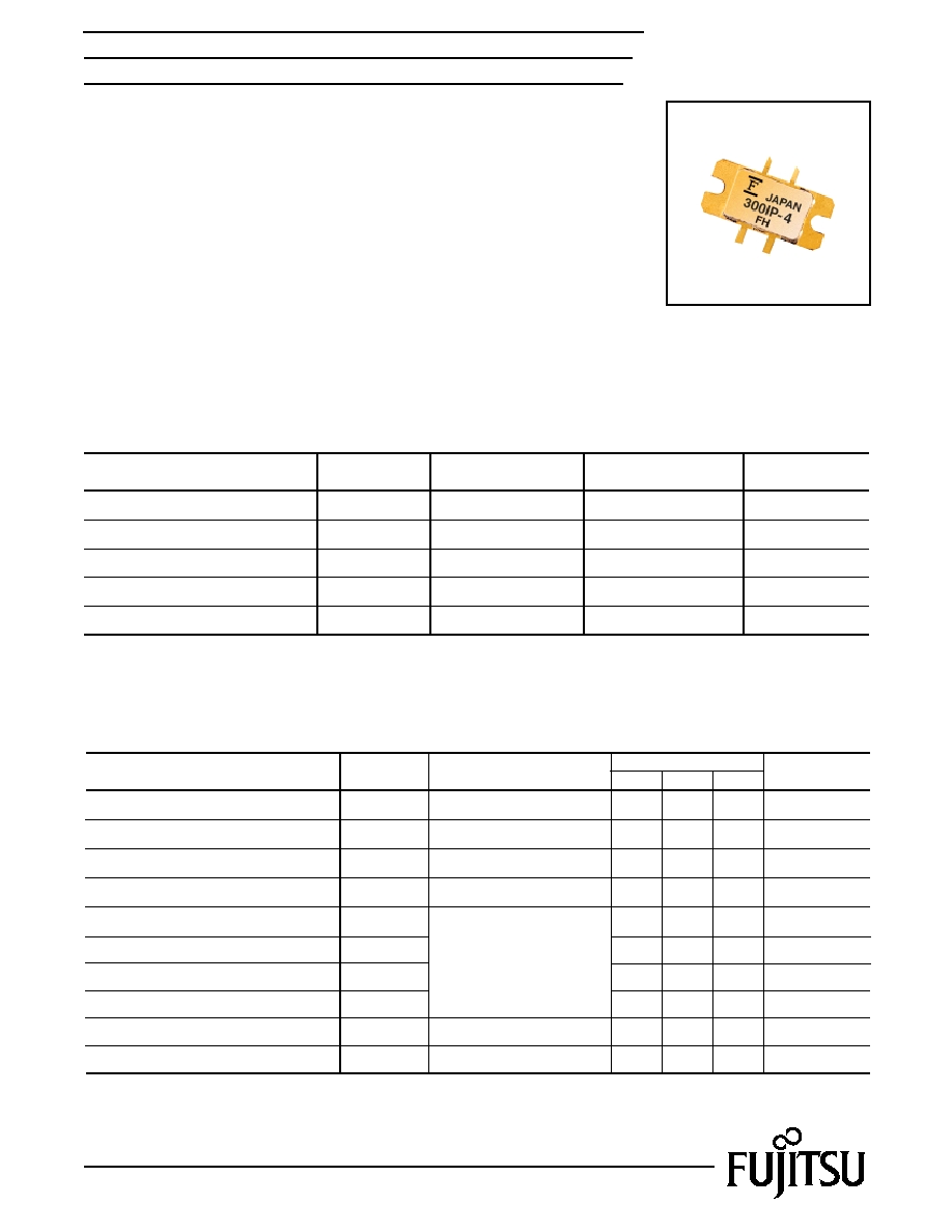
CASE STYLE: IP
Channel Temperature Rise
-
-
80
Note 2
∞
C
T
ch
Parameter
Drain-Source Voltage
Gate-Source Voltage
Total Power Dissipation
Storage Temperature
Channel Temperature
Symbol
V
DS
Tc = 25
∞
C
V
V
W
∞
C
∞
C
V
GS
P
T
T
stg
T
ch
Condition
107
-65 to +175
+175
-5
15
Rating
Unit
ABSOLUTE MAXIMUM RATINGS (Ambient Temperature Ta=25
∞
C)
Fujitsu recommends the following conditions for the reliable operation of GaAs FETs:
1. The drain-source operating voltage (VDS) should not exceed 10 volts.
2. The forward and reverse gate currents should not exceed 54.4 and -17.4mA respectively with
gate resistance of 25
.
3. The operating channel temperature (Tch) should not exceed 145
∞
C.
1
DESCRIPTION
The FLL300IP-4 is a 30 Watt GaAs FET that employs a push-pull design which
offers ease of matching, greater consistency and a broader bandwidth for high
power L-band amplifiers. This product is targeted to reduce the size and complexity
of highly linear, high power base station transmitting amplifiers. This new product is
uniquely suited for use in Wireless Local Loop (WLL) base station amplifiers as it
offers high gain, long term reliability and ease of use.
APPLICATIONS
∑ Solid State Base-Station Power Amplifier.
∑ WLL Communication Systems.
Edition 1.4
December 1999
FLL300IP-4

3
FLL300IP-4
S-PARAMETERS
VDS = 10V, IDS = 3.0A
FREQUENCY
S11
S21
S12
S22
(MHZ)
MAG
ANG
MAG
ANG
MAG
ANG
MAG
ANG
1000
.952
173.8
1.115
42.2
.007
23.4
.841
179.4
1100
.953
172.7
1.035
37.4
.007
35.9
.843
178.9
1120
.951
172.1
1.022
36.3
.007
40.2
.842
178.8
1300
.946
169.6
.918
26.9
.007
34.6
.846
177.4
1400
.942
168.4
.876
21.7
.008
25.6
.846
177.0
1500
.942
167.0
.843
16.4
.009
30.7
.845
175.8
1600
.936
165.2
.816
10.9
.008
30.2
.848
174.9
1700
.934
163.7
.799
5.3
.009
23.6
.847
174.2
1800
.928
162.1
.785
-.3
.010
28.1
.850
173.2
1900
.923
160.8
.778
-6.0
.010
23.9
.850
172.0
2000
.917
159.2
.779
-12.0
.011
22.2
.849
171.2
2100
.910
157.8
.783
-18.0
.012
16.0
.851
170.3
2200
.907
156.6
.793
-24.2
.012
13.7
.852
169.3
2300
.892
154.7
.812
-30.6
.013
12.9
.855
168.3
2400
.882
153.3
.834
-37.8
.013
6.9
.855
167.7
2500
.867
152.5
.868
-43.3
.014
-.8
.862
167.3
2600
.848
151.0
.915
-51.2
.014
-3.9
.865
166.6
2700
.822
149.7
.969
-59.3
.015
-9.3
.870
166.1
2800
.787
148.3
1.051
-68.7
.015
-8.2
.876
165.5
2900
.744
146.9
1.148
-79.7
.015
-16.1
.890
164.7
3000
.685
146.6
1.267
-92.5
.019
-27.9
.904
163.3
3100
.617
148.5
1.401
-107.9
.018
-45.8
.915
161.8
3200
.549
154.9
1.525
-126.8
.016
-63.3
.921
159.9
3300
.541
167.5
1.576
-148.6
.017
-86.5
.917
157.0
3400
.630
176.2
1.490
-172.0
.013
-114.9
.892
154.4
3500
.751
177.2
1.305
165.8
.008
-148.2
.864
153.8
3600
.840
174.1
1.088
146.8
.005
-179.3
.842
153.1
3700
.894
170.2
.886
130.5
.005
111.0
.832
153.2
3800
.928
166.9
.727
117.4
.007
88.7
.829
153.3
3900
.942
163.5
.599
105.5
.006
61.9
.830
152.8
4000
.951
160.6
.496
94.9
.008
54.4
.835
152.1
4100
.959
158.2
.421
85.5
.010
40.5
.839
151.3
4200
.958
155.5
.358
76.2
.010
31.5
.850
149.8
4300
.960
153.1
.307
68.0
.010
17.1
.859
148.4
4400
.957
150.5
.266
59.8
.011
24.3
.862
146.8
4500
.959
147.8
.233
52.1
.011
17.4
.868
144.7
4600
.958
145.3
.205
44.7
.012
16.5
.871
142.4
4700
.953
142.2
.180
37.8
.012
17.4
.884
140.0
4800
.957
139.1
.163
31.4
.013
17.9
.883
137.2
4900
.952
135.9
.148
24.9
.014
17.7
.896
134.9
5000
.955
132.3
.134
18.7
.015
16.5
.904
131.5
Note: This S-Parameter data shows measurements performed on a single-ended push-pull FET. These parameters should be used
to determine the calculated Push-Pull S-Parameter amplifier designs.
Download S-Parameters, click here

4
FLL300IP-4
Case Style "IP"
Metal-Ceramic Hermetic Package
18.6
±
0.2
(0.732)
45
∞
2
3
4
5
6
1
22
±
0.2
(0.866)
2.4
(0.094)
(0.039)
9.8
±
0.2
(0.386)
(0.102)
2.6
±
0.2
8.2
(0.332)
1.9
(0.075)
3.0
±
0.5 MIN.
(0.118)
3.0
±
0.5 MIN.
(0.118)
5.5MAX
(0.217)
13.8
±
0.2
(0.543)
13.3
(0.523)
2-R1.3
±
0.2
(0.051)
5
(0.197)
0.1
+0.05
-0.01
2-1.4
(0.055)
2-1
(0.039)
Unit: mm (inches)
1, 2: Gate
3, 6: Source
4, 5: Drain
Fujitsu Compound Semiconductor Products contain gallium arsenide
(GaAs) which can be hazardous to the human body and the environment.
For safety, observe the following procedures:
CAUTION
∑ Do not put these products into the mouth.
∑ Do not alter the form of this product into a gas, powder, or liquid
through burning, crushing, or chemical processing as these by-products
are dangerous to the human body if inhaled, ingested, or swallowed.
∑ Observe government laws and company regulations when discarding this
product. This product must be discarded in accordance with methods
specified by applicable hazardous waste procedures.
For further information please contact:
FUJITSU COMPOUND SEMICONDUCTOR, INC.
2355 Zanker Rd.
San Jose, CA 95131-1138, U.S.A.
Phone: (408) 232-9500
FAX: (408) 428-9111
www.fcsi.fujitsu.com
FUJITSU MICROELECTRONICS EUROPE, GmbH
Quantum Devices Division
Network House
Norreys Drive
Maidenhead, Berkshire SL6 4FJ
Phone:+44 (0)1628 504800
FAX:+44 (0)1628 504888
Fujitsu Limited reserves the right to change products and specifications without notice.
The information does not convey any license under rights of Fujitsu Limited or others.
© 1997 FUJITSU COMPOUND SEMICONDUCTOR, INC.
Printed in U.S.A. FCSI0797M200
