 | –≠–ª–µ–∫—Ç—Ä–æ–Ω–Ω—ã–π –∫–æ–º–ø–æ–Ω–µ–Ω—Ç: FLX257XV | –°–∫–∞—á–∞—Ç—å:  PDF PDF  ZIP ZIP |
1
Edition 1.3
July 1999
FLX257XV
GaAs FET & HEMT Chips
Item
Saturated Drain Current
Transconductance
Pinch-off Voltage
Gate Source Breakdown Voltage
Power-added Efficiency
Output Power at 1dB
Gain Compression Point
Power Gain at 1dB
Gain Compression Point
Symbol
IDSS
-
1000
1500
-
600
-
-1.0
-2.0
-3.5
-5
-
-
6.5
7.5
-
-
31
-
32.5
33.5
-
VDS = 5V, IDS = 50mA
VDS = 5V, IDS = 600mA
VDS = 5V, VGS = 0V
IGS = -50µA
VDS = 10V
IDS 0.6IDSS
f = 10GHz
mA
mS
V
dB
%
dBm
V
gm
Vp
VGSO
P1dB
G1dB
add
Thermal Resistance
-
8
10
Rth
Test Conditions
Unit
Limit
Typ.
Max.
Min.
ELECTRICAL CHARACTERISTICS (Ambient Temperature Ta=25∞C)
Note: RF parameter sample size 10pcs. criteria (accept/reject)=(2/3)
Channel to Case
∞C/W
The chip must be enclosed in a hermetically sealed environment for optimum performance and reliability.
DESCRIPTION
The FLX257XV chip is a power GaAs FET that is
designed for general purpose applications in the X-Band
frequency range as it provides superior power, gain, and
efficiency.
Fujitsu's stringent Quality Assurance Program assures the
highest reliability and consistent performance.
95
40
(Unit: µm)
40
56
Drain
Drain
Drain
Drain
Gate
Gate
Gate
Item
Drain-Source Voltage
Gate-Source Voltage
Total Power Dissipation
Storage Temperature
Channel Temperature
Symbol
VDS
VGS
15
-5
15.0
-65 to +175
175
Tc = 25∞C
V
V
W
∞C
∞C
Ptot
Tstg
Tch
Condition
Unit
Rating
ABSOLUTE MAXIMUM RATING (Ambient Temperature Ta=25∞C)
Fujitsu recommends the following conditions for the reliable operation of GaAs FETs:
1. The drain-source operating voltage (VDS) should not exceed 10 volts.
2. The forward and reverse gate currents should not exceed 17.8 and -1.2 mA respectively with
gate resistance of 200.
3. The operating channel temperature (Tch) should not exceed 145∞C.
FEATURES
∑ High Output Power: P1dB = 33.5dBm(Typ.)
∑ High Gain: G1dB = 7.5dB(Typ.)
∑ High PAE: add = 31%(Typ.)
∑ Proven Reliability
2
FLX257XV
GaAs FET & HEMT Chips
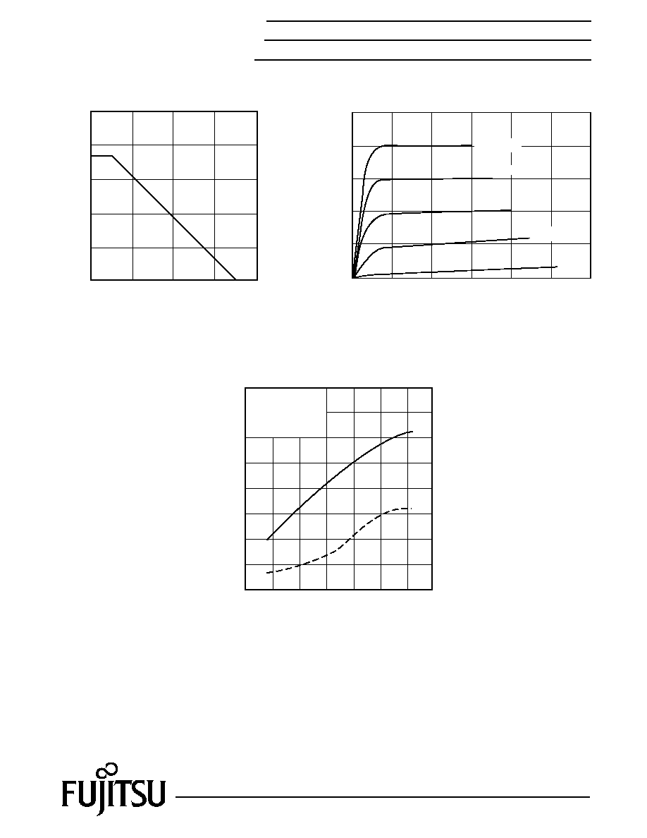
POWER DERATING CURVE
DRAIN CURRENT vs. DRAIN-SOURCE VOLTAGE
8
4
16
12
0
50
100
150
200
2
4
6
8
10
Case Temperature (∞C)
Drain-Source Voltage (V)
Total Power Dissipation (W)
31
33
35
29
27
25
23
17
19
21
23
25
27
Input Power (dBm)
Output Power (dBm)
1000
750
500
250
Drain Current (mA)
VGS =0V
-0.5V
-1.5V
-2.0V
-1.0V
OUTPUT POWER vs. INPUT POWER
VDS=10V
IDS0.6IDSS
f = 10GHz
add
Pout
40
30
20
10
add
(%)

3
S-PARAMETERS
VDS = 10V, IDS = 600mA
FREQUENCY
S11
S21
S12
S22
(MHZ)
MAG
ANG
MAG
ANG
MAG
ANG
MAG
ANG
100
.995
-35.2
14.385
161.0
.007
72.1
.390
-171.2
500
.963
-115.7
7.909
117.0
.020
32.2
.516
-168.2
1000
.953
-145.3
4.423
98.0
.022
18.4
.552
-170.1
2000
.951
-162.8
2.259
80.7
.022
11.8
.579
-169.1
3000
.951
-169.0
1.487
69.1
.022
11.3
.607
-167.1
4000
.953
-172.4
1.089
59.4
.021
13.3
.638
-165.5
5000
.955
-174.6
.846
50.6
.020
16.9
.671
-164.6
6000
.957
-176.3
.681
42.7
.019
22.1
.704
-164.2
7000
.959
-177.6
.562
35.5
.019
28.3
.735
-164.2
8000
.961
-178.8
.472
28.9
.019
35.2
.763
-164.5
9000
.963
-179.8
.402
22.9
.020
42.0
.789
-165.0
10000
.964
179.3
.345
17.5
.021
48.3
.811
-165.7
11000
.966
178.4
.300
12.6
.023
53.8
.831
-166.4
12000
.967
177.6
.262
8.3
.025
58.4
.849
-167.2
13000
.968
176.8
.230
4.4
.027
62.1
.864
-168.0
14000
.969
176.1
.202
1.0
.029
65.1
.878
-168.8
15000
.970
175.4
.179
-1.9
.032
67.5
.889
-169.6
16000
.971
174.7
.158
-4.4
.034
69.3
.900
-170.3
17000
.972
174.0
.140
-6.4
.037
70.8
.909
-171.0
18000
.972
173.3
.124
-7.8
.039
72.0
.916
-171.7
NOTE:*
The data includes bonding wires.
n: number of wires
Gate
n=8 (0.2mm length, 25µm Dia Au wire)
Drain n=8 (0.2mm length, 25µm Dia Au wire)
FLX257XV
GaAs FET & HEMT Chips
Download S-Parameters, click here
For further information please contact:
FUJITSU COMPOUND SEMICONDUCTOR, INC.
2355 Zanker Rd.
San Jose, CA 95131-1138, U.S.A.
Phone: (408) 232-9500
FAX: (408) 428-9111
www.fcsi.fujitsu.com
FUJITSU MICROELECTRONICS, LTD.
Compound Semiconductor Division
Network House
Norreys Drive
Maidenhead, Berkshire SL6 4FJ
Phone:+44 (0)1628 504800
FAX:+44 (0)1628 504888
Fujitsu Limited reserves the right to change products and specifications without notice.
The information does not convey any license under rights of Fujitsu Limited or others.
© 1998 FUJITSU COMPOUND SEMICONDUCTOR, INC.
Printed in U.S.A. FCSI0598M200
Fujitsu Compound Semiconductor Products contain gallium arsenide
(GaAs) which can be hazardous to the human body and the environment.
For safety, observe the following procedures:
CAUTION
∑ Do not put these products into the mouth.
∑ Do not alter the form of this product into a gas, powder, or liquid
through burning, crushing, or chemical processing as these by-products
are dangerous to the human body if inhaled, ingested, or swallowed.
∑ Observe government laws and company regulations when discarding this
product. This product must be discarded in accordance with methods
specified by applicable hazardous waste procedures.
4
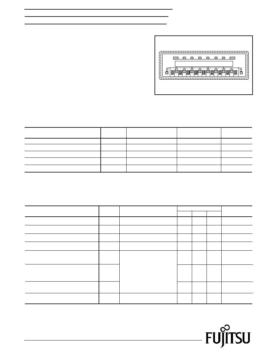
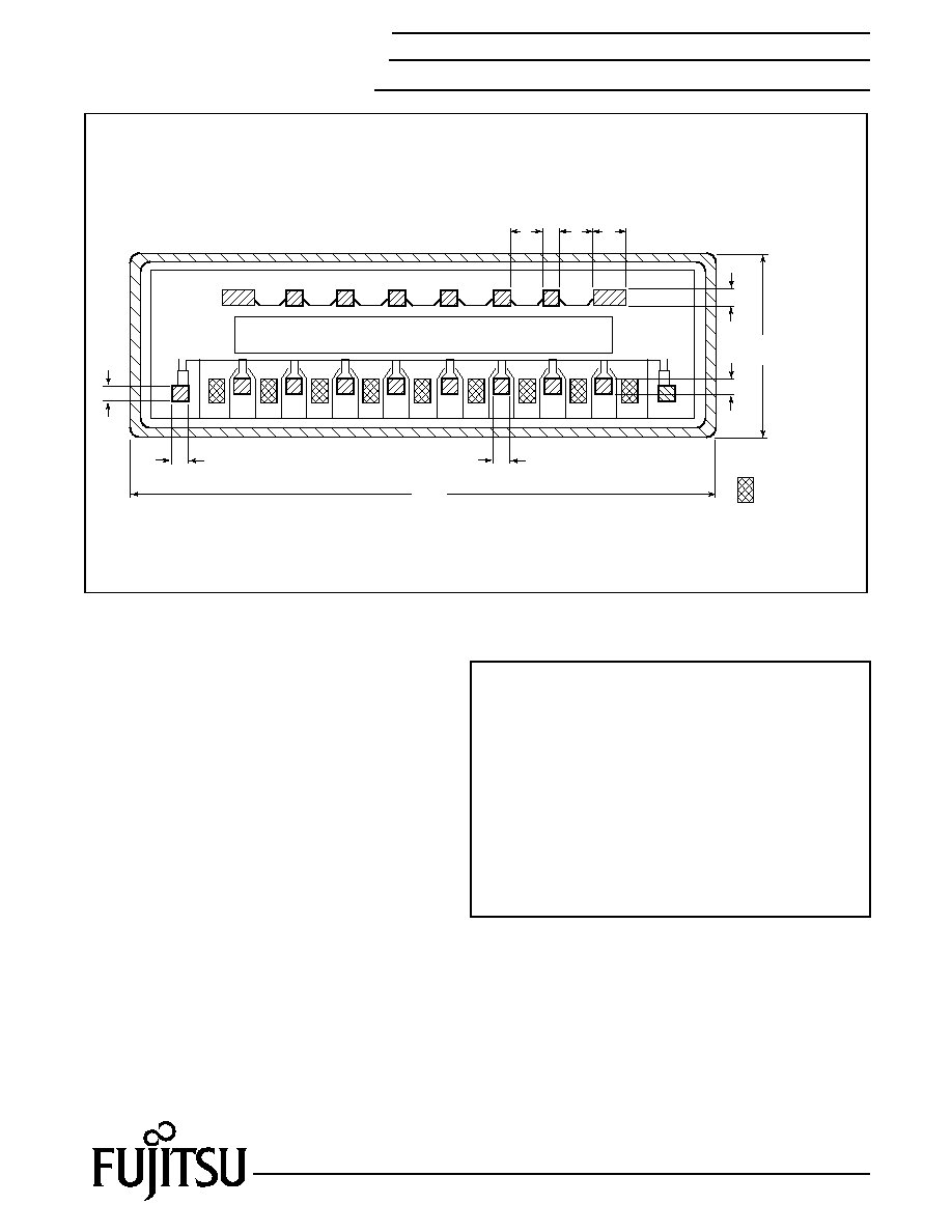
CHIP OUTLINE
Source electrodes are connected to
the PHS by Via-HOLE
Via-Hole
Die Thickness: 60±20µm
95
40
480
±
30
1770±30
(Unit: µm)
40
56
44
60
Drain
Drain
Drain
Drain
Gate
Gate
Gate
70
60
44
(Unit: µm)
106
60
106
128
FLX257XV
GaAs FET & HEMT Chips