Parameter
Supply Voltage
Operating Temperature*
Symbol
-7.0 to 0
(VDD = 0V)
-40 to +85
V
°C
Input Voltage
VSS to VDD
V
Peak Current Control Voltage
VSS -2.0 to VSS +2.1
VSS -2.0 to VSS +2.1
V
VIP
VIB
Bias Current Control Voltage
V
DIN, DIN, CIN
VSS
Storage Temperature
-40 to +125
°C
Tstg
TOP
Ratings
Unit
ABSOLUTE MAXIMUM RATINGS
(*) Lower limit temperature corresponds to the ambient temperature and higher limit temperature
corresponds to the case (the bottom of the case) temperature.
· Modulation Current and Bias Current Monitor
· Duty Ratio Monitor
· Duty Ratio Control
· Single Power Supply: -5.2V
· Separated Peak Current and Bias Current Outputs
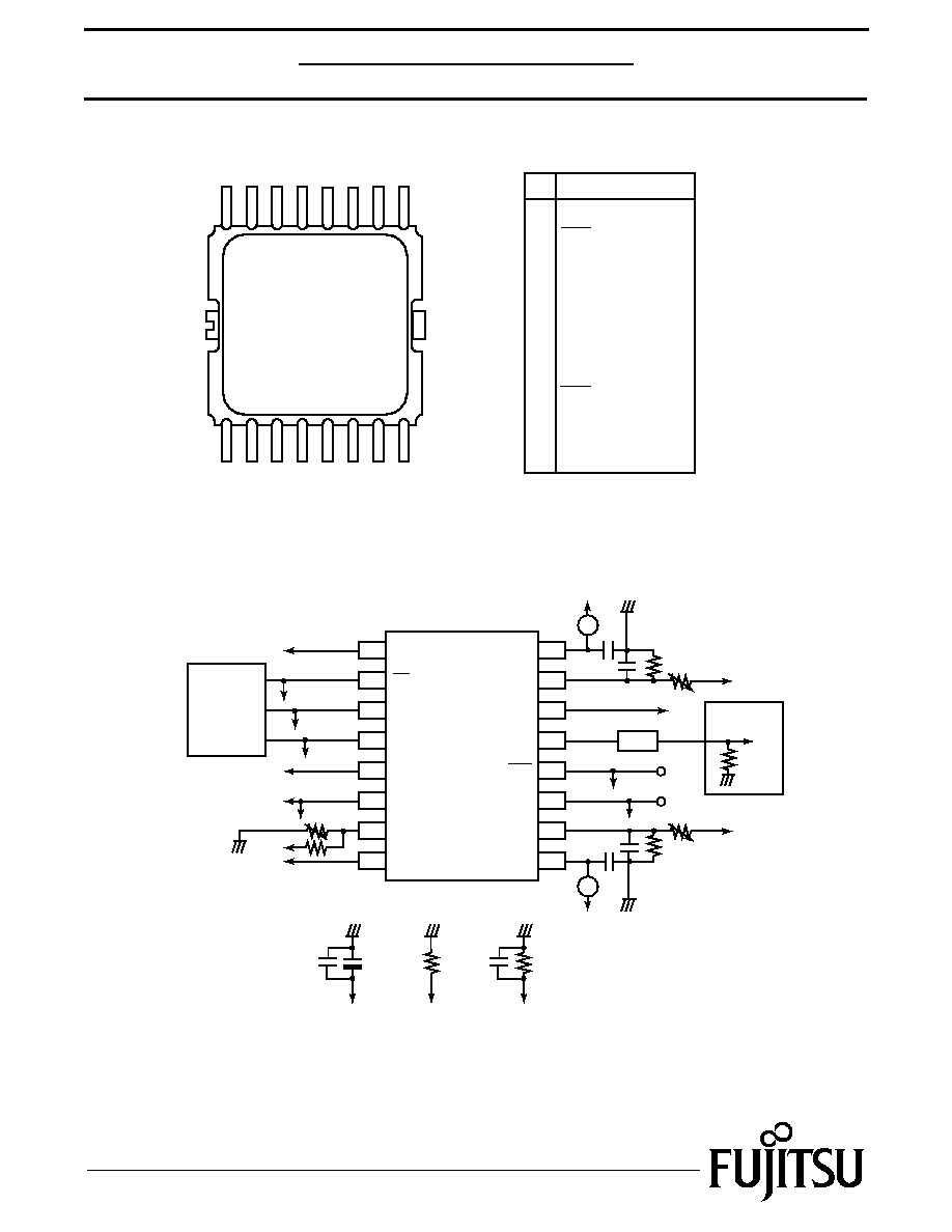
· Small Package: SSOP-16
Parameter
Power Supply Voltage
Data & Clock Input
Peak Current Control Voltage
Bias Current Control Voltage
Output Shutdown Control Voltage
Selector Control Voltage
Symbol
-5.2 -4.94
-1.0
-0.9
-1.7
-1.6
-1.0
-1.6
-0.7
-1.9
VSS
-
VSS
+2.1
VSS
VSS
+2.1
-
-1.7
-1.9
-0.7
-0.9
V
V
V
V
V
V
VDD
-
-
V
V
Open
-
-
-
VIH
VIL
Output enable
Output disable (Shutdown)
D-F/F active
D-F/F inactive
VIP
VIB
VSD
VSS
Test Conditions
Unit
Limit
Typ.
Max.
Min.
RECOMMENDED OPERATING CONDITIONS
VSE
-5.72
(VDD = 0V)
DESCRIPTION
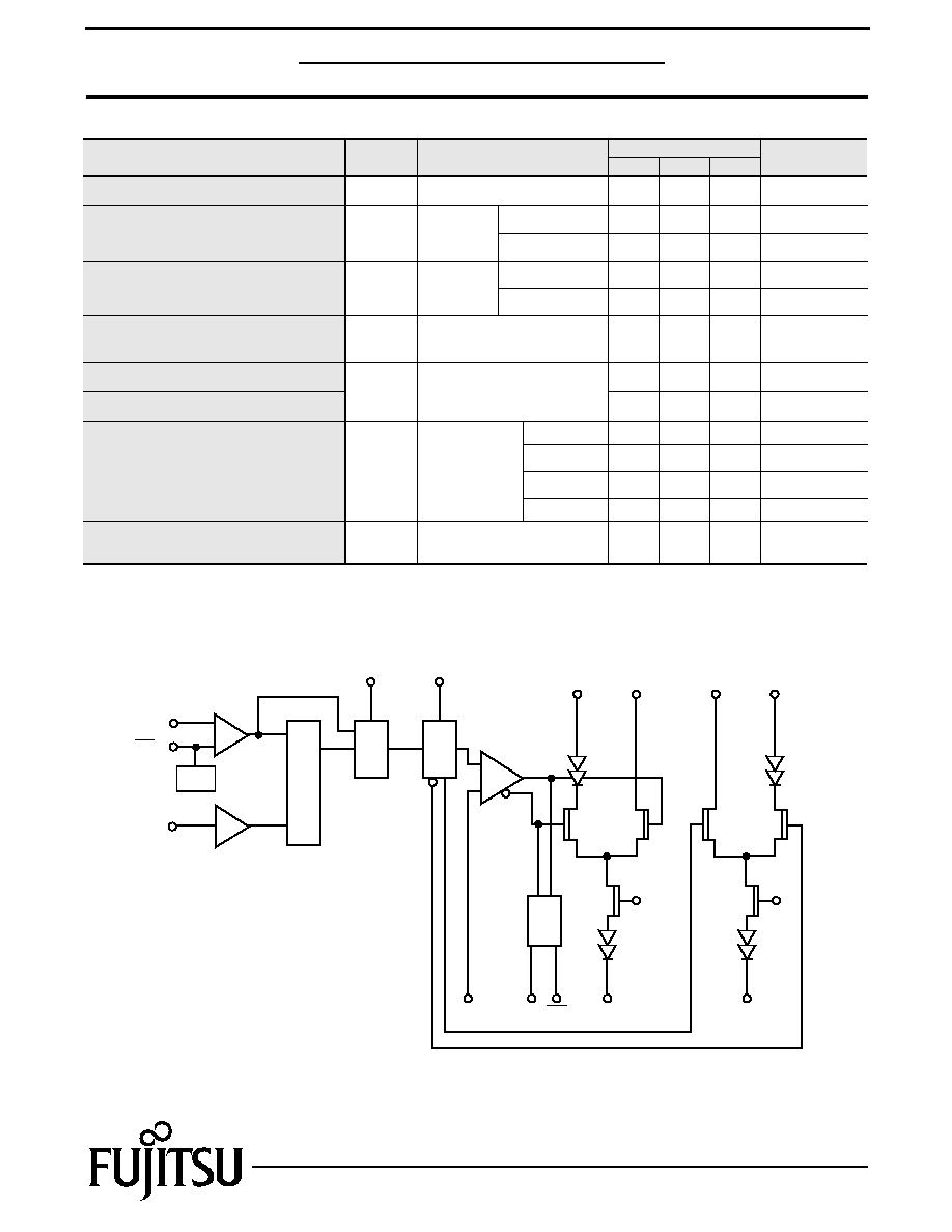
The FMM3171VI is a laser driver IC for up to 1.2Gb/s optical transmission
systems. The GaAs MES-FET IC process allows for high speed operation
with low power consumption. There are two data inputs options; a comple-
mentary input or a single-ended input using a selectable D-F/F. The output
duty ratio can be set by adjusting the input reference voltage (Vref). The
differential mark-density monitor (Mmk) output proportional to the peak cur-
rent output signal. The peak current and bias current output is disabled by
the shutdown terminal, which is ECL compatible. Logic "high" causes the out-
put to be disabled. The High speed turn-on and turn-off is accomplished by a very
low compute time constant. The amount of peak current and bias current are monitored by the current
flow at lp and lb terminal which must be connected to VSS. This FMM3171VI is an excellent choice
use as a laser driver for OC-3/OC-12/OC-24
and STM1/STM4 transmitters.
FEATURES
· ECL Compatible Data Input
· Built in D-F/F (Optional)
· Complementary Data Input (Optional)
· Modulation Current: 0 to 70mA
· Bias Current: 0 to 70mA
· Output Shutdown Function
1
Edition 1.2
June 2000
VI
1.25Gb/s GaAs
Laser Driver
FMM3171VI
4
1.25Gb/s GaAs
Laser Driver
FMM3171VI
Fujitsu Compound Semiconductor Products contain gallium arsenide
(GaAs) which can be hazardous to the human body and the environment.
For safety, observe the following procedures:
CAUTION
· Do not put this product into the mouth.
· Do not alter the form of this product into a gas, powder, or liquid
through burning, crushing, or chemical processing as these by-products
are dangerous to the human body if inhaled, ingested, or swallowed.
· Observe government laws and company regulations when discarding this
product. This product must be discarded in accordance with methods
specified by applicable hazardous waste procedures.
For further information please contact:
FUJITSU COMPOUND SEMICONDUCTOR, INC.
Americas & R.O.W.
2355 Zanker Rd.
San Jose, CA 95131-1138, U.S.A.
Phone: (408) 232-9500
FAX: (408) 428-9111
www.fcsi.fujitsu.com
FME, QDD
Fujitsu Microelectronics Europe GmbH
Quantum Devices Division
Network House
Norreys Drive
Maidenhead, Berkshire SL6 4FJ
United Kingdom
TEL: +44 (0) 1628 504800
FAX: +44 (0) 1628 504888
FUJITSU QUANTUM DEVICES
SINGAPORE PTE LTD.
Hong Kong Branch
Rm. 1101, Ocean Centre, 5 Canton Rd. Tsim Sha Tsui,
Kowloon, Hong Kong
TEL: +852-23770226
FAX: +852-23763269
FUJITSU QUANTUM DEVICES LIMITED
Global Business Division
Global Sales Support Department
Shinjuku Daiichiseimei Building, 2-7-1 Nishishinjuku,
Shinjuku-ku, Tokyo, 163-0721, Japan
TEL: +81-3-5322-3356
FAX: +81-3-5322-3398
Fujitsu Limited reserves the right to change products and specifications without notice.
The information does not convey any license under rights of Fujitsu Limited or others.
© 2000 FUJITSU COMPOUND SEMICONDUCTOR, INC.
Printed in U.S.A. FCSI0200M200
(2.0)
(0.9)
(0.25)
6.4
5.0
0.7
0
.7
5.5
1.2
0.15
4.55
0.65
0.18
(0.4)
5.6
(3.3)
(3.2)
(0.45)
( 2.8)
(3.1)
(3.6)
(3.9)
y
16
9
1
8
0.13
M
0.1
Ground Pin
Heat Sink
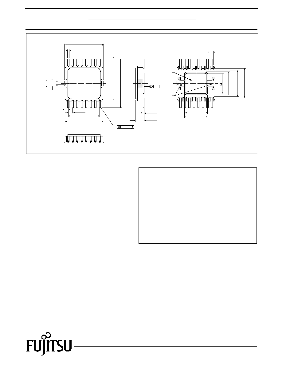
Unit: mm
"VI" PACKAGE
UNIT: mm