 | ÐлекÑÑоннÑй компоненÑ: MB1503 | СкаÑаÑÑ:  PDF PDF  ZIP ZIP |
/home/web/doc/html/fujitsu/180331
Sept. 1995
Edition 1.0a
DATA SHEET
1
Copyright
©
1994 by FUJITSULIMITED
The Fujitsu MB1503 is a serial input phase-locked loop (PLL) frequency synthesizer with a
pulse-swallow function. A stand-by mode is provided to limit power consumption during
intermittent operation.
The MB1503 is configured of a 1.1GHz dual-modulus prescaler with 128/129 divide ratio,
control signal generator, 16-bit shift register, 15-bit latch, programmable reference divider
(binary 14-bit programmable reference counter), 1-bit switch counter, phase comparator
with phase conversion function, charge pump, crystal oscillator, 19-bit shift register, 18-bit
latch, programmable divider (binary 7-bit swallow counter and binary 11-bit programmable
counter), analog switches, and an intermittent operation control circuit that selects the
operating or stand-by mode depending on the power-save control input state (PS).
The MB1503 operates from a single +5 V supply. Fujitsu's advanced technology achieves
an Icc of 8mA, typical. The stand-by mode current consumption is just 100
µ
A.
Features
·
High operating frequency
: f
IN
= 1.1GHz (P
IN
= 10dBm)
·
Pulse-swallow function
: High-speed dual-modulus prescaler with 128/129
divide ratio
·
Low supply current
: I
CC
= 8mA typ. at 5V
·
Power-saving stand-by mode : 100
µ
A
·
Serial input, 18-bit programmable divider consisting of:
Binary 7-bit swallow counter
: 0 to 127
Binary 11-bit programmable counter : 16 to 2,047
·
Serial input 15-bit programmable reference divider consisting of:
Binary 15-bit programmable reference counter: 8 to 16,383
1-bit switch counter sets prescaler divide ratio
·
On-chip analog switch for fast lock-up
·
On-chip charge pump
·
Wide operating temperature range: 40 to +85
°
C
·
Plastic 16pin dual inline package (Suffix : P)
Plastic 16pin small outline package (Suffix : PF)
ABSOLUTE MAXIMUM RATINGS (See NOTE)
Ratings
Symbol
Value
Unit
V
CC
0.5 to +7.0
V
Supply Voltage
V
P
V
CC
V
P
10.0
V
Output Voltage
V
OUT
0.5 to V
CC
+0.5
V
Output Current
I
OUT
±
10
mA
Storage Temperature
Tstg
55 to +125
°
C
LOW-POWER PLL FREQUENCY SYNTHESIZER WITH
POWER SAVE FUNCTION (1.1GHz)
MB1503
PLASTIC PACKAGE
(FPT-16P-M06)
This device contains circuitry to protect the inputs
against damage due to high static voltages or electric
fields. However, it is advised that normal precautions be
taken to avoid application of any voltage higher than
maximum rated voltages to this high impedance circuit.
NOTE: Permanent device damage may occur if the above Absolute Maximum
Ratings are exceeded. Functional operation should be restricted to the
conditions as detailed in the operational sections of this data sheet. Exposure
to absolute maximum rating conditions for extended periods may affect device
reliability.
PLASTIC PACKAGE
(DIP-16P-M04)

MB1503
2
PIN ASSIGNMENT
OSC
IN
1
16
PS
OSC
OUT
2
15
f
R
V
P
3
14
f
P
V
CC
4
13
BiSW
D
O
5
12
FC
GND
6
11
LE
LD
7
10
Data
f
IN
8
9
Clock
(TOP VIEW)
MB1503
3
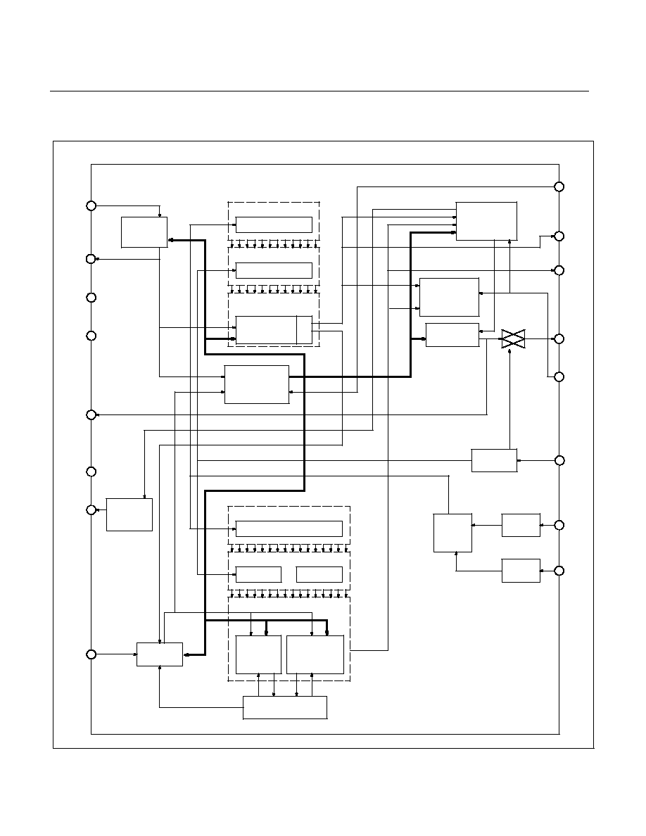
BLOCK DIAGRAM
S
W
OSC
IN
OSC
OUT
V
P
V
CC
Oscillator
Lock
Detection
Circuit
16-bit Shift Register
16-bit Shift Register
15-bit Latch
15-bit Latch
Programmable
Reference Divider
Binary 14-bit
Reference
Counter
Intermittent
Operation
Control Circuit
Phase
Comparator
Phase
Characteristics
Changing
Circuit
Charge
Pump
BiSW
Data
Schmitt
Trigger
Schmitt
Trigger
Schmitt
Trigger
1-bit
Control
Latch
19-bit Shift Register
19-bit Shift Register
7-bit Latch
18-bit Latch
11-bit Latch
Binary 7-bit
Swallow
Counter
Programmable Divider
Binary 11-bit
Programmable
Counter
Prescaler
Control Circuit
To Lock Detector
PS1
PS1
From
Phase
Comparator
PS1
PS1
PS1
MC
SW
From
Phase
Comparator
From Charge
Pump
PS1
Prescaler
Output
1
2
3
4
D
O
5
GND
6
LD
7
f
IN
8
Clock
9
10
LE
11
FC
12
13
f
P
14
f
R
15
PS
16
MB1503
4
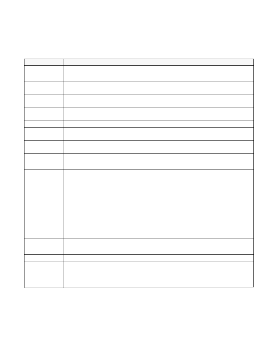
PIN DESCRIPTION
Pin No. Pin Name
I/O
Description
1
OSC
IN
I
Programmable reference divider input
Oscillator input
An external crystal is connected to this pin.
2
OSC
OUT
O
Oscillator output
An external crystal is connected to this pin.
3
V
P
Power supply input for charge pump and analog switch
4
V
CC
Power supply
5
D
O
O
Charge pump output
The phase of the charge pump is reversed depending on the FC input.
6
GND
Ground
7
LD
O
Phase comparator output
The output level is high when LD is locked. The output level is low when LD is unlocked.
8
f
IN
I
Prescaler input
Connection with an external VCO should be done by AC coupling.
9
Clock
I
Clock input for 19-bit and 16-bit shift registers
Data is shifted into the shift register on the rising edge of the clock.The Schmitt trigger is
contained.
10
Data
I
Serial data input using binary code
The last bit of the data is a control bit.
When the control bit is high, data is transmitted to the 15-bit latch.
When it is low, data is transmitted to the 18-bit latch.The Schmitt trigger input is involved.
11
LE
I
Load enable signal input
When LE is high, the data of the shift register are transferred to a latch, depending on the
control bit in the serial data. At the same time, an internal analog switch turns on and the output
of the internal charge pump is connected to the BiSW pin.The Schmitt trigger input is involved.
12
FC
I
Phase select input of phase comparator (with internal pull-up resistor)
When FC is low, the characteristics of the charge pump and phase comparator are reversed.
The FC input signal is also used to control the f
OUT
pin (test pin) of f
R
or f
P.
13
BiSW
O
Analog switch output
BiSW is usually in the high-impedance state. When the switch is turned on (LE is high), the
state of the internal charge pump is output.
14
f
P
O
Monitor pin of programmable counter output
15
f
R
O
Monitor pin of reference counter output
16
PS
I
Power save signal input
Set PS low while the system is powered (never use pin 16 as it is opened)
PS = High
: Operation mode
PS = Low
: Stand-by mode
MB1503
5
FUNCTIONAL DESCRIPTIONS
Pulse swallow function
The divide ratio can be calculated using the following equation:
f
VCO
= [(M x N) + A] x f
OSC
÷
R (A < N)
f
VCO
: Output frequency of external voltage controlled oscillator (VCO)
N
: Preset divide ratio of binary 11-bit programmable counter (16 to 2,047)
A
: Preset divide ratio of binary 7-bit swallow counter (0
A
127)
f
OSC
: Output frequency of the reference frequency oscillator
R
: Preset divide ratio of binary 14-bit programmable reference counter (8 to 16,383)
M
: Preset divide ratio of modules prescaler (128)
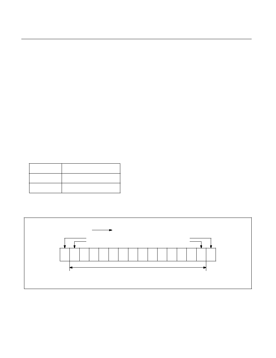
Serial data input
Serial data is input using the Data, Clock, and LE pins. Serial data controls the 15-bit programmable reference divider and 18-bit
programmable divider separately.
Binary serial data is input to the Data pin.
One bit of data is shifted into the internal shift registers on the rising edge of the clock. When the load enable pin is high or open, stored
data is latched depending on the control data as follows:
Control data
Destination of serial data
H
15-bit latch
L
18-bit latch
(a)
Programmable reference divider ratio
The programmable reference divider consists of a 15-bit latch and a 14-bit reference counter. The serial 16-bit data format is
shown below:
S
S
S
S
S
S
S
S
S
S
S
S
S
S
C
1
2
3
4
5
6
7
8
9
10
11
12
13
14
SW
Direction of data shift
Control bit
LSB
Divide ratio setting bit for prescaler
MSB
Divide ratio setting bit for programmable reference counter