 | –≠–ª–µ–∫—Ç—Ä–æ–Ω–Ω—ã–π –∫–æ–º–ø–æ–Ω–µ–Ω—Ç: MB1509 | –°–∫–∞—á–∞—Ç—å:  PDF PDF  ZIP ZIP |
Sept. 1995
Edition 3.0a
DATA SHEET
1
Copyright
©
1995 by FUJITSU LIMITED and FUJITSU MICROELECTRONICS, INC.
Rating
Symbol
Value
Unit
NOTE:
Permanent device damage may occur if the above Absolute Maximum Ratings
are exceeded. Functional operation should be restricted to the conditions as
detailed in the operational sections of this data sheet. Exposure to absolute
maximum rating conditions for extended periods may affect device reliability.
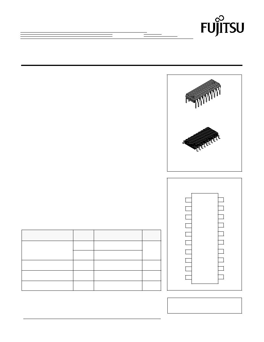
PIN ASSIGNMENT
This device contains circuitry to protect the inputs against
damage due to high static voltages or electric fields. However,
it is advised that normal precautions be taken to avoid
application of any voltage higher than maximum rated voltages
to this high impedance circuit.
TOP
DUAL SERIAL INPUT PLL FREQUENCY SYNTHESIZER
ABSOLUTE MAXIMUM RATINGS (see NOTE)
MB1509
DUAL SERIAL INPUT PLL FREQUENCY SYNTHESIZER
WITH 400MHz PRESCALER
The Fujitsu MB1509 is a 400MHz dual serial input PLL (Phase Locked) frequency synthesizer
designed for cordless telephone application.
The MB1509 has two PLL circuits on a single chip: one for transmit and the other for reception.
Separate power supply pins are provided for the transmit and reception PLL circuits. Transmit
PLL contains a low sensitivity charge pump for ease of modulation and reception PLL contains a
high sensitivity charge pump for faster lock up time.
The MB1509 incorporates two 400 MHz dual modulus prescalers to enable implemention of a
pulse swallow function.
It operates supply voltage of 3.0V typ. and dissipates 8mA typ. of current realized through the
use of Fujitsu's unique U-ESBIC Bi-CMOS technology.
∑
High operating frequency: fin = 400MHz
∑
Low power supply voltage: V
CC
= 2.7 to 5.5V
∑
Low power supply current: I
CC
= 8mA typ, @3V.
∑
Wide operating temperature: T
A
= ≠40 to 85
∞
C
∑
Two charge pumps
Low sensitivity charge pump for transmit
High sensitivity charge pump for reception
∑
Plastic 20-pin dual in line package (Suffix: -P)
Plastic 20-pin flat package (Suffix: -PF)
PLASTIC PACKAGE
DIP-20P-M02
1
2
3
4
5
6
20
19
18
17
16
15
GND
V
CC
V
PLASTIC PACKAGE
FPT-20P-M01
Power Supply Voltage
Clock
OSC
OUT
fin
1
OSC
IN
V
CC1
fr
Data
LE
fin
2
V
CC2
fp
≠0.5 to 7.0
V
P
V
CC
to 10.0
V
OUT
V
Output Voltage
≠0.5 to V
CC
+0.5
I
OUT
mA
Output Current
±
10
T
STG
∞
C
Storage Temperature
≠55 to +125
7
8
9
10
14
13
12
11
LD
1
V
P1
D
O1
BS
1
LD
2
V
P2
D
O2
BS
2
VIEW
MB1509
2
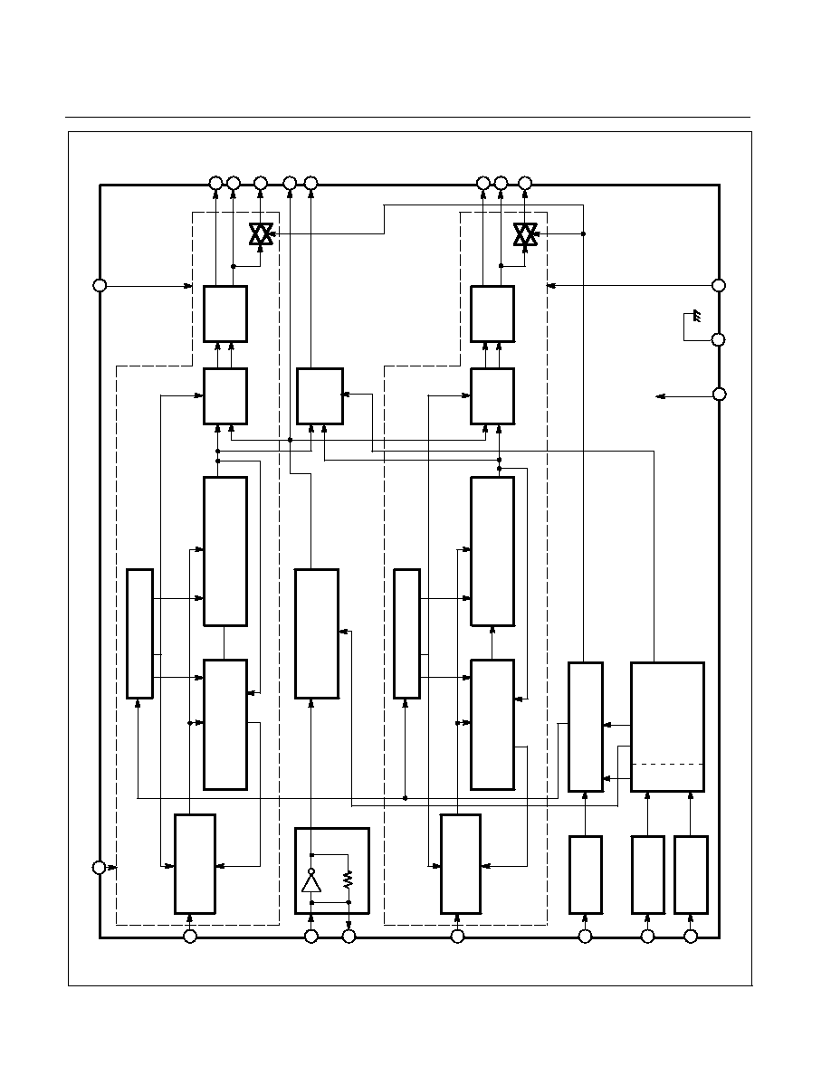
MB1509 BLOCK DIAGRAM
8
7
9
10
Charge
Pump
Phase
Detector
Binary
11-bit
Program-
mable
Counter
Binary
7-bit
Swallow
Counter
Prescaler
20-bit
latch
fp
monitor
output
selector
5
6
Reference
Counter
(512,
1024)
4
2
3
15
14
12
11
17
18
Charge
Pump
Phase
Detector
Binary
11-bit
Program-
mable
Counter
Binary
7-bit
Swallow
Counter
20-bit
latch
Latch
Selec-
tor
23-bit shift
register
Schmitt
Circuit
19
Schmitt
Circuit
20
Schmitt
Circuit
13
16
1
Crystal
Oscillator
Prescaler
CNT
RECEP-
TION
SECTION
TRANSMIT
SECTION

MB1509
3
TRANSMIT/RECEPTION BLOCK
∑
20-bit latch
∑
Programmable divider consisting of:
Binary 7-bit swallow counter (Divide ratio: 0 to 127)
Binary 11-bit programmable counter (Divide ratio: 16 to 2047)
∑
Phase detector with phase polarity change function
∑
400MHz dual modulus prescaler (Divide ratio: 32/33, 64/65)
∑
Charge pump
COMMON BLOCK
∑
23-bit shift register
∑
Programmable divider consisting of:
Reference counter (Divide ratio: 512, 1024)
(Divide frequency = 25kHz, 12.5kHz (Crystal oscillator frequency = 12.8MHz)
∑
Crystal oscillator
∑
fp monitor output selector
∑
Latch selector
∑
Schmitt circuits
∑
Analog switches
BLOCK DESCRIPTIONS
MB1509
4
Pin No. Pin Name
PIN DESCRIPTIONS
GND
Descriptions
1
Ground.
I/O
≠
2
I
OSC
IN
OSC
OUT
Oscillator input pin.
Oscillator output pin.
A crystal is connected between OSC
IN
pin and OSC
OUT
pin.
3
4
I
fin
1
Prescaler input pin of transmit section.
The connection with VCO should be AC connection.
O
5
≠
V
CC1
Power supply voltage input pin of transmit section.
When power is OFF, latched data of transmit section is cancelled.
6
O
fr
Monitor pin for programmable reference divider output.
7
O
LD1
Lock detect signal output pin of transmit section.
Condition
LD pin output level
Lock H
Unlock
L
8
≠
V
P1
Power supply voltage input for charge pump and analog switch of transmit section.
9
O
D
O1
Charge pump output pin of transmit section.
Phase characteristics of the phase detector can be reversed depending upon FC-bit setting.
10
O
BS1
Analog switch output pin of transmit section.
Usually this pin is high-impedance state. During SW is ON (LE = high), charge pump output is con-
nected to this pin.
11
O
BS2
Analog switch output pin of reception section.
Usually this pin is high-impedance state. During SW is ON (LE = high), charge pump output is con-
nected to this pin.
12
O
D
O2
Charge pump output pin of reception section.
Phase characteristics of the phase detector can be reversed depending upon FC-bit setting.
13
≠
V
P2
Power supply voltage input for charge pump and analog switch of reception section.
14
O
LD2
Lock detect signal output pin of reception section.
Condition
LD pin output level
Lock H
Unlock
L
15
O
fp
Monitor pin for programmable divider output.
This pin outputs divided frequency of transmit section or reception section depending upon FP bit set-
ting.
FP bit
Output
H
Transmit section (fp1)
L
Reception section (fp2)
MB1509
5
Pin No. Pin Name
PIN DESCRIPTIONS (Continued)
Descriptions
I/O
16
≠
V
CC2
Power supply voltage input pin for reception section, programmable reference divider, shift register,
and crystal oscillator.
When power is OFF, latched data of reception section and reference counter is cancelled.
19
I
Data
Serial data input pin of 23-bit shift register. This pin involves a schmitt trigger circuit.
The stored data in the shift register is transferred to either transmit section or reception section de-
pending upon a control data.
Control bit data
The destination of data
H
Latch of transmit section
L
Latch of reception section
17
I
fin
2
Prescaler input pin of reception section.
The connection with VCO should be AC conneciton.
18
I
LE
Load enable input pin. This pin involves a schmitt trigger circuit.
When this pin is high, the data stored in the shift register is transferred into the latch depending on a
control data.
At this moment, charge pump output signal is output from BS pin since internal analog swith becomes
ON.
20
I
Clock
Clock input pin of 23-bit shift register. This pin involves a schmitt trigger circuit.
On rising edge of the clock shifts one bit of data into the shift register.
FUNCTIONAL DESCRIPTIONS
The divide ratio can be calculated using the following equation:
f
VCO
= {(M x N) + A} x f
OSC
˜
R (A < N)
f
VCO
: Output frequency of external voltage controlled ocillator (VCO)
M:
Preset divide ratio of dual modulus prescaler (32 or 64)
N:
Preset divide ratio of binary 11-bit programmable counter (16 to 2047)
A:
Preset divide ratio of binary 7-bit swallow counter (0
v
A
v
127)
f
OSC
: Reference oscillator frequency
R:
Preset divide ratio of reference counter (512 or 1024)