1
DS04-21309-4E
FUJITSU SEMICONDUCTOR
DATA SHEET
ASSP
Serial Input PLL Frequency
Synthesizer
MB1511
s
DESCRIPTION
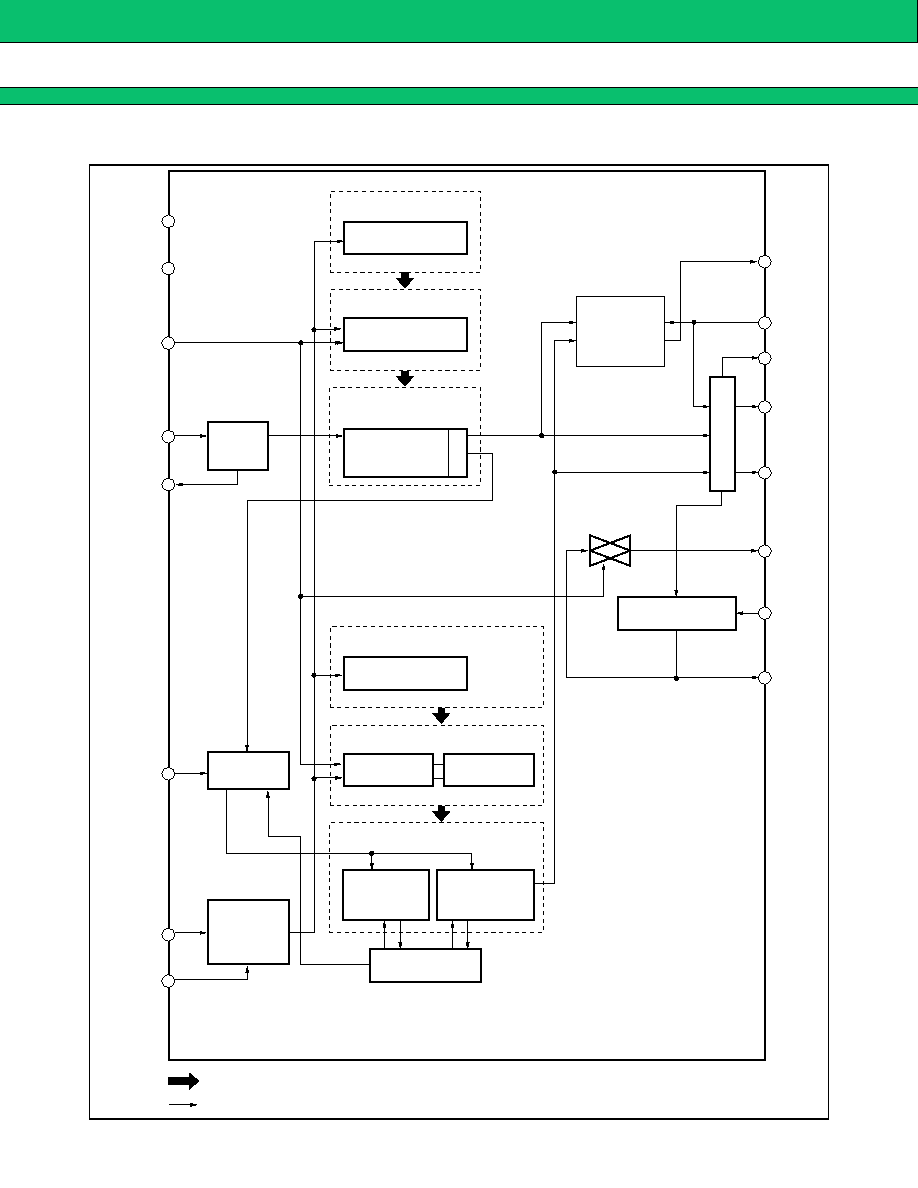
The Fujitsu MB1511 is a single chip serial input PLL frequency synthesizer designed for VHF tuner and cellular
telephone applications.
It contains a 1.1 GHz dual modulus prescaler which enables pulse swallow function, and an analog switch to
speed up lock up time.
It operates supply voltage of 3.0 V typ. and dissipates 7 mA typ. of current realized through the use of Fujitsu's
unique U-ESBIC Bi-CMOS technology.
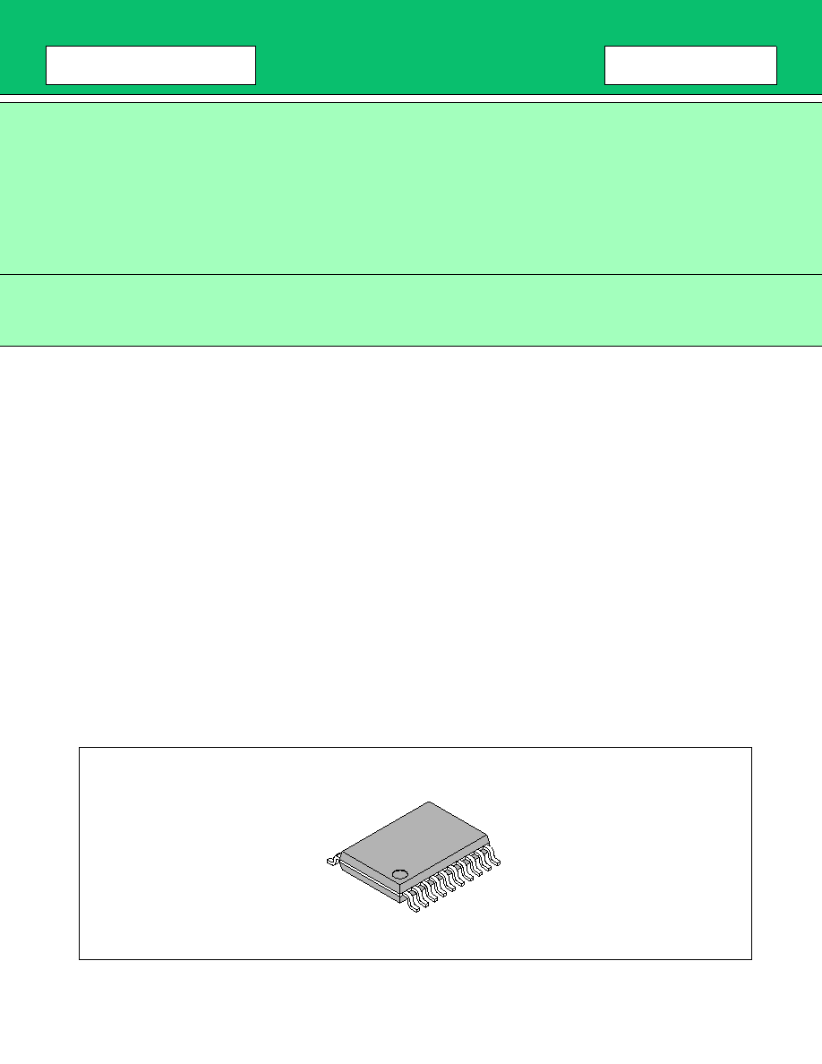
The MB1511 is housed in SSOP package, this enables high integration.
s
FEATURES
∑ Low power supply voltage: V
CC
= 2.7 to 5.5 V
∑ High operating frequency: f
IN MAX
= 1.1 GHz (V
IN MIN
= ≠10dBm)
∑ Pulse swallow function: 64/65 or 128/129
∑ Low supply current: I
CC
= 7 mA typ.
Serial input 18-bit programmable divider consisting of:
Binary 7-bit swallow counter: 0 to 127
Binary 11-bit programmable counter: 16 to 2047
∑ Serial input 15-bit programmable reference divider consisting of:
Binary 14-bit programmable reference counter: 8 to 16383
1-bit switch counter (SW) sets divide ratio of prescaler
(Continued)
s
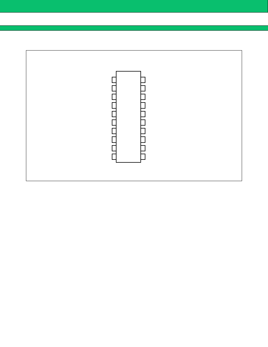
PACKAGE
(FPT-20P-M03)
20 pin, Plastic SSOP
4
MB1511
s
PIN DESCRIPTION
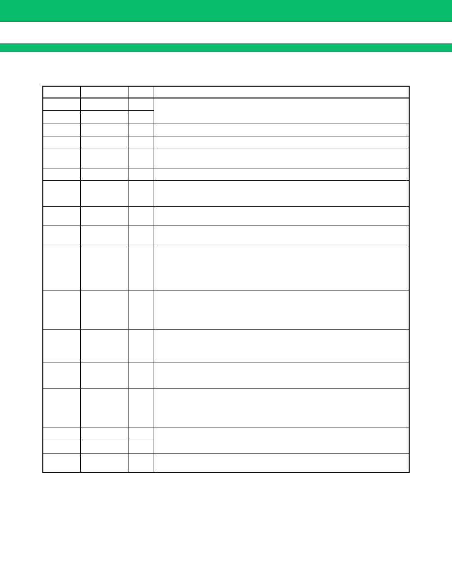
Pin No.
Pin Name
I/O
Functions
1
OSC
IN
I
Oscillator input.
Oscillator output.
A crystal is placed between OSC
IN
and OSC
OUT
.
3
OSC
OUT
O
4
V
P
--
Power supply input for charge pump and analog switch.
5
V
CC
--
Power supply voltage input.
6
D
O
O
Charge pump output.
The characteristics of charge pump is reversed depending upon FC input.
7
GND
--
Ground.
8
LD
O
Phase comparator output.
Normally this pin outputs high level. While the phase difference of fr and fp
exists, this pin outputs low level.
10
fin
I
Prescaler input.
The connection with an external VCO should be AC connection.
11
Clock
I
Clock input for 19-bit shift register and 16-bit shift register.
On rising edge of the clock shifts one bit of data into the shift registers.
13
Data
I
Binary serial data input.
The last bit of the data is a control bit which specified destination of shift reg-
isters.
When this bit is high level and LE is high level, the data stored in shift regis-
ter is transferred to 15-bit latch. When this bit is low level and LE is high
level, the data is transferred to 18-bit latch.
14
LE
I
Load enable input (with internal pull up resistor).
When LE is high or open, the data stored in shift register is transferred into
latch depending upon the control bit. At the time, internal charge pump out-
put is connected to BiSW pin because internal analog switch becomes ON
state.
15
FC
I
Phase select input of phase comparator (with internal pull up resistor).
When FC is low level, the characteristics of charge pump, phase comparator
is reversed.
FC input signal controls fout pin (test pin) output level, fr or fp.
16
BiSW
O
Analog switch output.
Usually BiSW pin is set high-impedance state. When internal analog switch
is ON (LE pin is high level), this pin outputs internal charge pump output.
17
fout
O
Minitor pin of phase comparator input.
fout pin outputs either programmable reference divider output (fr) or pro-
grammable divider output (fp) depending upon FC pin input level.
FC = H: It is the same as fr output level.
FC = L: It is the same as fp output level.
18
P
O
Output for external charge pump.
The characteristics are reversed according to FC input.
P pin is N-channel open drain output.
20
R
O
2, 9
12, 19
NC
--
No connection.