 | –≠–ª–µ–∫—Ç—Ä–æ–Ω–Ω—ã–π –∫–æ–º–ø–æ–Ω–µ–Ω—Ç: MB1517A | –°–∫–∞—á–∞—Ç—å:  PDF PDF  ZIP ZIP |
DS04≠21325≠1aE
DATA SHEET
1
MB1517A
ASSP
2.0 GHz High≠Speed Tuning PLL Frequency Synthesizer
The Fujitsu MB1517A is a serial input phase-locked loop (PLL) frequency synthesizer with
a pulse-swallow function. MB1517A achieves the low noise performance as well as the
high≠speed lock-up which is required for digital mobile communications.
The MB1517A can operate from a single +3 V supply. Fujitsu's advanced technology
achieves an Icc of 12 mA (typical) as well as 100
µ
A (typical) at power down mode.
FEATURES
∑
High operating frequency
: f
IN
= 2.0 GHz (P
IN
= ≠10 dBm)
∑
Pulse-swallow function
: High-speed two-modulus prescaler with selectable
64/65 and 128/129 divide ratios
∑
Low supply current
: I
CC
= 12 mA typ. at 3 V
∑
Power saving funtion
: I
PS
= 100
µ
A typ.
∑
Serial input, 18-bit programmable divider consisting of:
Binary 7-bit swallow counter
: 0 to 127
Binary 11-bit programmable counter : 5 to 2,047
∑
Serial input 17-bit programmable reference divider consisting of:
Binary 14-bit programmable reference counter: 6 to 16,383
1-bit switch counter sets prescaler divide ratio
1-bit power saving function control
1-bit LD/font switch
∑
On-chip high performance charge pump circuit and phase comparator, achieving
high-speed lock-up and low phase noise
∑
Two types of phase comparator outputs selectable
On-chip charge pump output
Output for an external charge pump
∑
Wide operating temperature range: ≠40 to +85
∞
C
∑
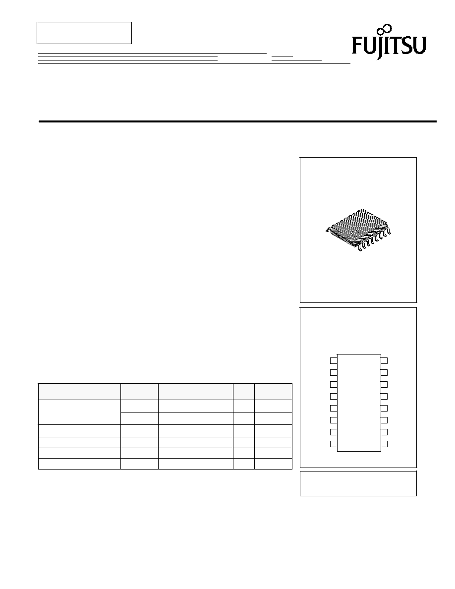
Plastic 16≠pin SSOP (shrink small outline) package
ABSOLUTE MAXIMUM RATINGS (See NOTE)
Parameters
Symbol
Rating
Unit
Remark
V
CC
≠0.5 to +5.0
V
Supply voltage
V
P
V
CC
to 5.5
V
Output voltage
V
O
≠0.5 to V
CC
+0.5
V
Open drain voltage
V
OOP
≠0.5 to 6.0
V
P, LD/fout
Output current
I
O
±
10
mA
Storage temperature
Tstg
≠55 to +125
∞
C
This device contains circuitry to protect the inputs against
damage due to high static voltages or electric fields.
However, it is advised that normal precautions be taken
to avoid application of any voltage higher than maximum
rated voltages to this high impedance circuit.
NOTE:
Permanent device damage may occur if the above Absolute Maximum Ratings are
exceeded. Functional operation should be restricted to the conditions as detailed in the
operational sections of this data sheet. Exposure to absolute maximum rating conditions
for extended periods may affect device reliability.
OSC
IN
1
16
R
OSC
OUT
2
15
P
V
P
3
14
LD/f
OUT
V
CC
4
13
NC
D
O
5
12
FC
GND
6
11
LE
Xf
IN
7
10
Data
f
IN
8
9
Clock
PIN ASSIGNMENT
(TOP VIEW)
(FPT≠16P≠M05)
Plastic SSOP, 16 pin
(FPT≠16P≠M05)
MB1517A
2
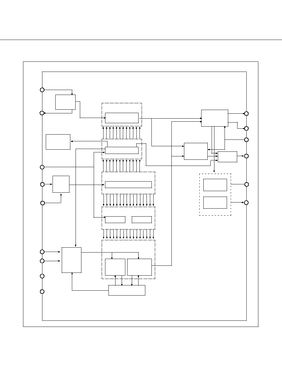
BLOCK DIAGRAM
OSC
IN
OSC
OUT
V
P
V
CC
Crystal
Oscillator
circuit
17-bit latch
17-bit latch
Programmable
reference divider
Binary 14-bit
reference counter
Phase
comparator
Charge
pump
LD
/f
OUT
Data
1-bit
control
latch
19-bit shift register
19-bit shift register
7-bit latch
18-bit latch
11-bit latch
Binary 7-bit
swallow
counter
Programmable divider
Binary 11-bit
programmable
counter
Control circuit
1
2
3
4
D
O
5
GND
6
f
IN
8
Clock
9
10
LE
11
FC
12
14
P
15
R
16
Prescaler
64/65,
128/129
Super
charger II
DATA
LE
SW
MC
fp
fp
fp
fR
fR
FC
FC
f
R
/f
P
selector
Intermittent
mode control
(power save)
PS
LE
LD/fout
selector
LD
LDS
Xf
IN
7
MB1517A
3
PIN DESCRIPTION
Pin No. Pin name
I/O
Description
1
OSC
IN
I
Programmable reference divider input
Oscillator input
Connection for external crystal or TCXO.
2
OSC
OUT
O
Oscillator output
Connection for external crystal.
3
V
P
≠
Power supply input for the internal charge pump
4
V
CC
≠
Power supply
5
D
O
O
Charge pump output
Phase characteristics of the charge pump can be reversed by FC input.
6
GND
≠
Ground
7
Xfin
I
Complementary input of the prescaler
Xfin pin should be grounded via a capacitor.
8
f
IN
I
Prescaler input
Connection with an external VCO should be done AC coupled.
9
Clock
I
Clock input for 19-bit shift register
Data is shifted into the shift register on the rising edge of the clock.
10
Data
I
Serial data input using binary code
The last bit of the data is a control bit.
When the control bit is high, data is transmitted to the 17-bit latch.
When it is low, data is transmitted to the 18-bit latch.
11
LE
I
Load enable signal input
When LE is high, the data of the shift register are transferred to a latch, according to the
control bit in the serial data.
12
FC
I
Phase switch input for phase comparator
When FC is low, the characteristics of the charge pump and phase comparator are reversed
The FC input signal is also used to control the f
OUT
pin (test pin) output (f
R
or f
P
).
13
NC
≠
No connection
14
LD/f
OUT
O
Lock detector output / Phase comparator monitoring output
This is a N-ch open drain output.
Either of the outputs is selected by LDS bit of the serial data.
a)Lock detector output : at lock state .... LD = "H"
at unlock stae .. LD = "L"
b)Monitoring output : Phase comparator input signals (f
P
, f
R
) can be monitored.
15
P
O
Phase comparator output for an external charge pump
Phase of the output is reversed according to FC input.
P pin is a N-ch open drain output.
16
R
O
Phase comparator output for an external charge pump
Phase of the output is reversed depending on FC input.
MB1517A
4
FUNCTION DESCRIPTIONS
Pulse swallow function
The divide ratio can be calculated using the following equation:
f
VCO
= [(P x N) + A] x f
OSC
˜
R (A < N)
f
VCO
: Output frequency of external voltage controlled oscillator (VCO)
N
: Preset divide ratio of binary 11-bit programmable counter (5 to 2,047)
A
: Preset divide ratio of binary 7-bit swallow counter (0
A
127)
f
OSC
: Output frequency of the reference frequency oscillator
R
: Preset divide ratio of binary 14-bit programmable reference counter (6 to 16,383)
P
: Preset divide ratio of modules prescaler (64 or 128)
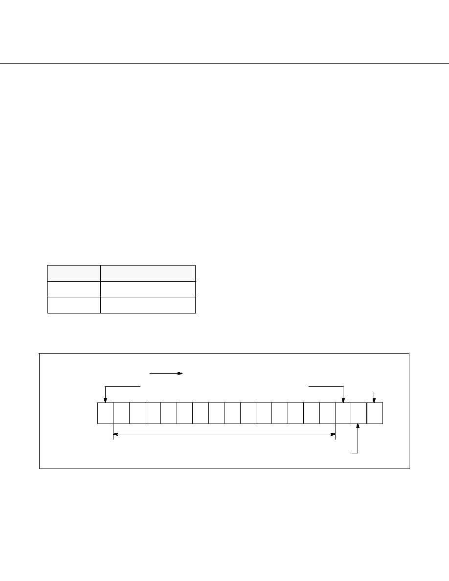
Serial data input
Serial data is processed using the Data, Clock, and LE pins. Serial data controls the 17-bit programmable reference divider and 18-bit
programmable divider separately.
Binary serial data is entered via the Data pin.
One bit of data is shifted into the internal shift register on the rising edge of the clock. When the load enable pin is high, stored data is
latched according to the control data as follows:
Control data
Destination of serial data
H
17 bit latch
L
18 bit latch
(a)
Programmable reference divider ratio
The programmable reference divider consists of a 18-bit shift register, a 17-bit latch and a 14-bit reference counter. The serial
18-bit data format is shown below:
R
R
R
R
R
R
R
R
R
R
R
R
R
R
C
1
2
3
4
5
6
7
8
9
10
11
12
13
14
SW
PS LDS
Direction of data shift
Control bit(LSB)
Divide ratio setting bit for
the prescaler
Divide ratio setting bit for the programmable reference counter
Power saving control bit
LD/fout select bit
(MSB)
MB1517A
5
∑
14-bit programmable reference counter divide ratio
Divide ratio
R
R
R
R
R
R
R
R
R
R
R
R
R
R
R
14
13
12
11
10
9
8
7
6
5
4
3
2
1
6
0
0
0
0
0
0
0
0
0
0
0
1
1
0
7
0
0
0
0
0
0
0
0
0
0
0
1
1
1
∑
∑
∑
∑
∑
∑
∑
∑
∑
∑
∑
∑
∑
∑
∑
16383
1
1
1
1
1
1
1
1
1
1
1
1
1
1
(Divide ratio = 6 to 16,383)
Notes: 1. Divide ratios less than 6 are prohibited.
2. SW : This bit selects the divide ratio of the prescaler.
Low: 128 or 129
High: 64 or 65
3. R1 to R14: These bits select the divide ratio of the programmable reference counter (6 to 16,383).
4. C: Control bit: Set high.
5. PS: This bit controls power saving mode.
High : Nomal operation
Low : Power saving mode
6. LDS: This bit controls LD/fout output signal
High : fout signal (f
R
or f
P
) is selected and output via LD/fout pin.
Low : Lock detect signal is selected and output via LD/fout pin.
7. Start data input with MSB first .
(b)
Programmable divider divide ratio
The programmable divider consists of a 19-bit shift register, a 18-bit latch, a 7-bit swallow counter, and a 11-bit programmable
counter. The serial 19-bit data format is shown below:
S
S
S
S
S
S
S
N
N
N
N
N
N
N
N
N
N
N
C
1
2
3
4
5
6
7
1
2
3
4
5
6
7
8
9
10
11
Direction of data shift
Control bit
LSB
MSB
Divide ratio setting bit for
swallow counter
Divide ratio setting bit for programmable counter