 | –≠–ª–µ–∫—Ç—Ä–æ–Ω–Ω—ã–π –∫–æ–º–ø–æ–Ω–µ–Ω—Ç: MB1518 | –°–∫–∞—á–∞—Ç—å:  PDF PDF  ZIP ZIP |
DATA SHEET
DS04≠21311≠2aE
Copyright
©
1994 by FUJITSU LIMITED and FUJITSU MICROELECTRONICS, INC.
MB1518
Serial Input PLL Frequency Synthesizer With
On≠Chip 2.5GHz Prescaler
This device contains circuitry to protect the inputs against
damage due to high static voltages or electric fields.
However, it is advised that normal precautions be taken to
avoid application of any voltage higher than maximum
rated voltages to this high impedance circuit.
Rating
Symbol
Value
Unit
NOTE:
Permanent device damage may occur if the above Absolute Maximum Ratings
are exceeded. Functional operation should be restricted to the conditions as
detailed in the operational sections of this data sheet. Exposure to absolute
maximum rating conditions for extended periods may affect device reliability.
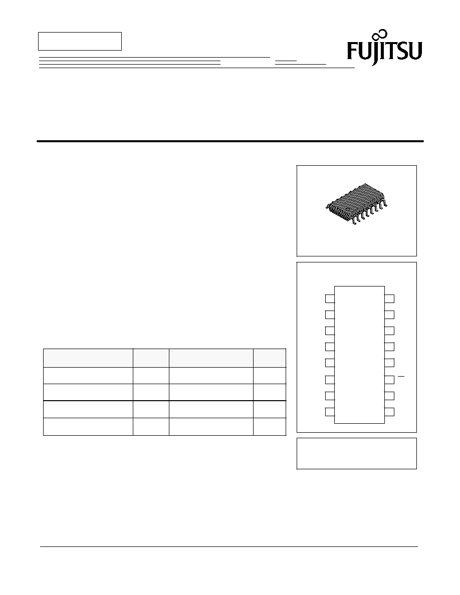
PIN ASSIGNMENT
TOP
ABSOLUTE MAXIMUM RATINGS (see NOTE)
The Fujitsu MB1518 with an on chip 2.5 GHz dual modulus prescaler is a serial input PLL (Phase
Locked Loop) frequency synthesizer with pulse swallow function. It is well suited for BS tuner,
CATV system applications.
It operates supply voltage of 5.0V typ. and dissipates 16mA typ. of current realized through the
use of Fujitsu's unique U-ESBIC Bi-CMOS technology.
∑
Power supply voltage: V
CC
= 4.5 to 5.5V
∑
High operating frequency: f
in
= 2.5GHz (P
in
= ≠4dBm)
∑
2.5GHz dual modulus prescaler: P = 512/528
∑
Low power supply current: I
CC
= 16mA typ.
∑
Programmable reference divider : R = 512
∑
Programmable divider consisting of:
Binary 5≠bit swallow counter (A = 0 to 31)
Binary 9-bit programmable counter (N = 32 to 511)
∑
Wide operating temperature: T
a
= ≠40 to +85
∞
C
∑
Plastic 16-pin flat package (Suffix: ≠PF)
PLASTIC PACKAGE
FPT-16P-M06
1
2
3
4
5
16
15
14
13
12
V
CC
V
Power Supply Voltage
Data
Clock
LE
V
CC1
OSC
IN
LD
f
OUT
V
CC2
≠0.5 to 7.0
V
O
0.5 to V
CC
+0.5
I
O
mA
Output Current
"
10
T
STG
∞
C
Storage Temperature
≠55 to +125
6
7
8
11
10
9
OSC
OUT
GND1
D
01
VIEW
Output Voltage
V
f
IN
GND2
f
IN
FC
D
02
MB1518
2
16
LD
15
f
OUT
14
13
V
CC2
f
in
12
11
10
9
GND2
f
in
FC
D
O2
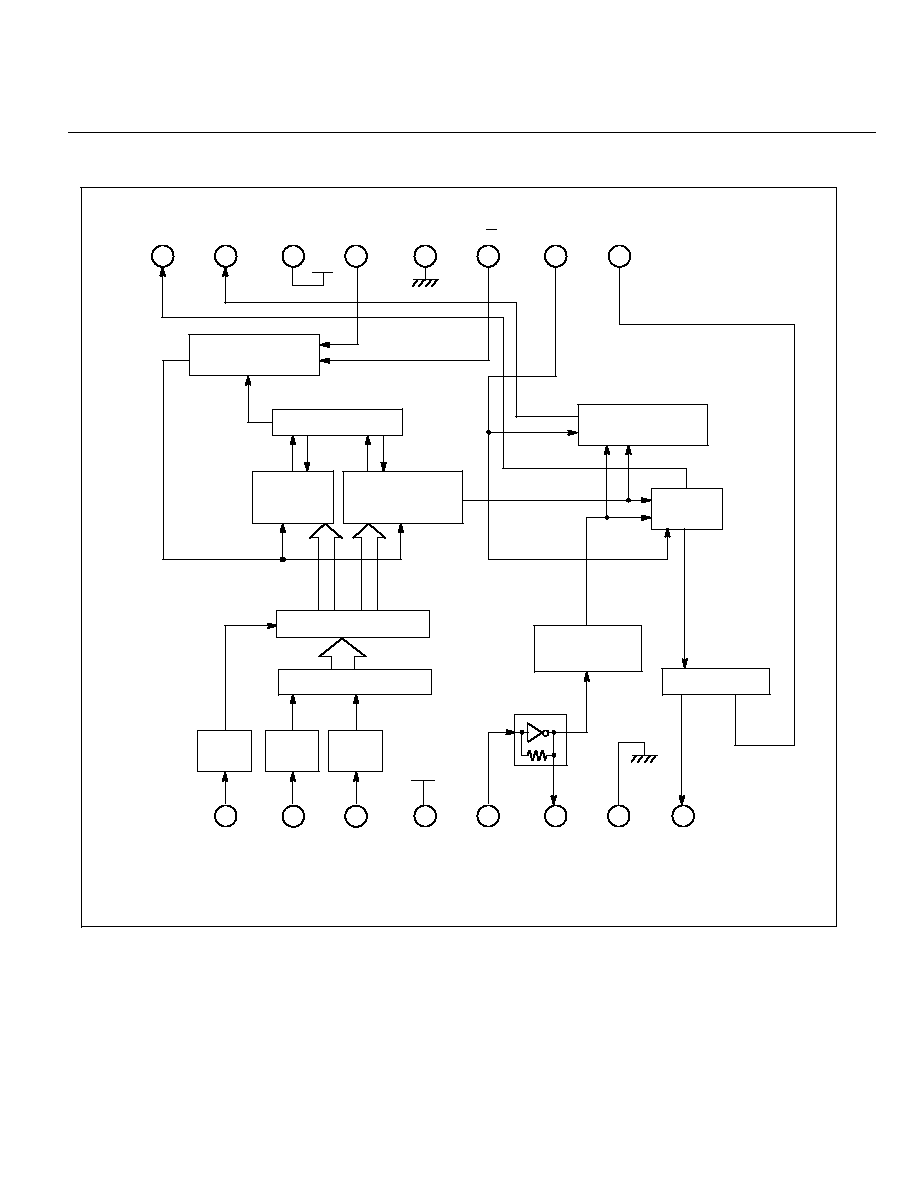
Prescaler
(P=512/528)
Monitor Frequency
Selector
Phase
Detector
Control Circuit
5-bit Swallow
Counter
(A=0~31)
9-bit Programmable
Counter
(N=32~511)
5
9
14-bit latch
14
14-bit Shift Register
1
2
3
4
5
6
7
8
LE
Data
Clock
V
CC1
OSC
in
OSC
out
GND1
D
01
Schmitt
Trigger
Schmitt
Trigger
Reference Counter
(R=512)
Schmitt
Trigger
Charge Pump
Crystal
Oscillator
MD
f
OUT
FC
f
r
f
p
BLOCK DIAGRAM
MB1518
3
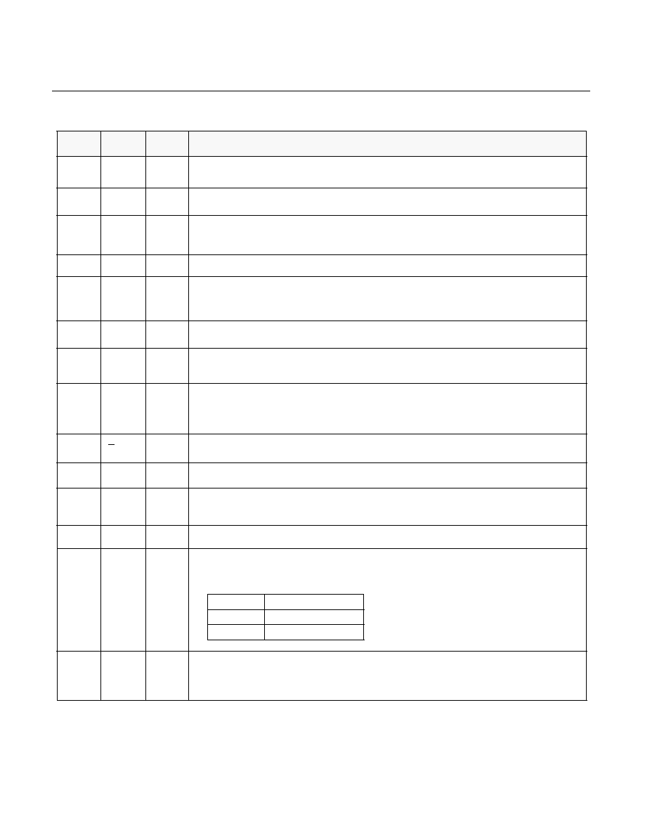
Pin No.
Pin Name
PIN DESCRIPTIONS
FC
Descriptions
10
Phase select input pin of the phase detector. This pin involves an internal pull up resistor.
When this pin is low, characteristics of the charge pump and phase detector can be reversed. This
input also selects f
OUT
pin output level, either fr or fp. Please see on page 6.
I/O
I
5
I
OSC
IN
OSC
OUT
Oscillator input pin.
Oscillator output pin.
A crystal is connected between OSC
IN
pin and OSC
OUT
pin.
6
2
I
Data
Serial data of binary code input pin. This pin involves a schmitt trigger circuit.
O
3
I
V
CC1
Clock input pin of the 14≠bit shift register. This pin involves a schmitt trigger circuit.
On rising edge of the clock shifts one bit of the data into the shift register.
4
≠
PLL power supply voltage input pin.
7
≠
GND1
PLL ground pin.
8
O
D
O1
Charge pump output pins.
Phase characteristics can be reversed depending upon FC pin input level.
Phase detector output pin.
Normally this pin outputs high. While the phase difference between fr and fp exists, this pin outputs low.
11
I
Load enable input pin. This pin involves a schmitt trigger circuit.
When this pin is high, the data stored in the shift register is transferred into the latch.
12
≠
GND2
14
≠
V
CC2
Prescaler power supply voltage input pin.
15
O
f
OUT
Monitor pin of the phase detector input.
f
OUT
pin outputs either of the programmable reference divider output frequency fr or programmable
divider output frequency fp depending upon the FC pin input level.
FC pin
fout output signal
H
fr
L
fp
16
O
LD
LE
I
1
Clock
9
O
D
O2
Complementary input pin of f
in
. Please connect to GND through a capacitor.
f
in
Prescaler ground pin.
13
I
f
in
Prescaler input pin,
This signal is input with AC coupled.
MB1518
4
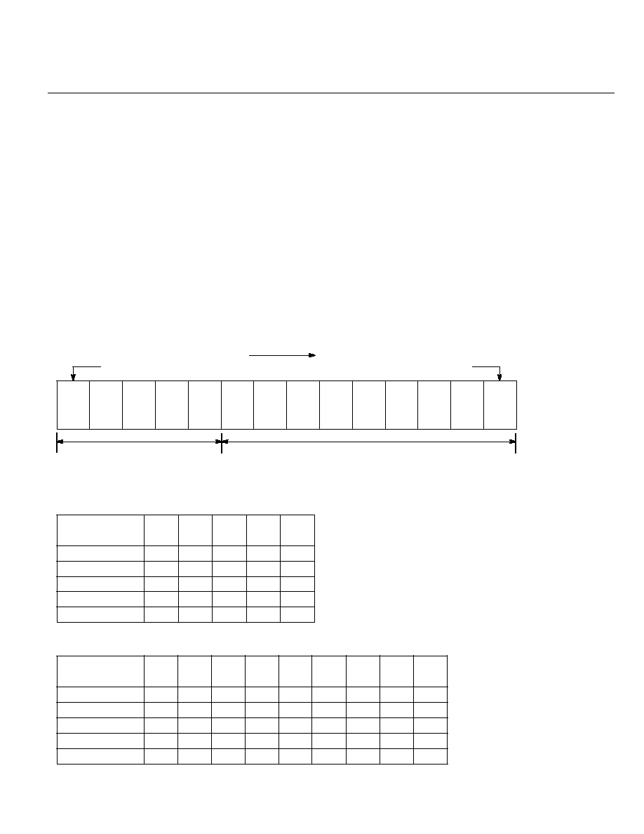
SERIAL DATA I NPUT
On rising edge of the clock shifts one bit of the data into the shift register.
When the load enable is high, the data stored in the shift register is transferred to the latch.
1
FUNCTIONAL DESCRIPTIONS
2
3
4
5
A
6
7
8
9
N
LSB
Data Input Flow
14 bit of serial data formit is shown below.
A
A
A
A
1
2
3
4
5
N
N
N
N
N
N
N
N
Divide ratio of swallow
counter setting bit
Divide ratio of programmable
counter setting bit
Divide ratio can be set using the following equation:
f
VCO
= {(P x N) + (16 x A)} x f
OSC
˜
R
f
VCO
: Output frequency of an external voltage controlled oscillator (VCO)
P:
Preset divide ratio of an internal dual modulus prescaler (512)
N:
Preset divide ratio of binary 9-bit programmable counter (32 to 511)
A:
Preset divide ratio of binary 5-bit swallow counter (0 to 31)
f
OSC
: Reference oscillator frequency
R:
Preset divide ratio of reference counter (512)
DIVIDE RATIO SETTING
5-bit swallow counter divide ratio (A1 to A5)
9-bit programmable counter divide ratio (N1 to N9)
5
A
4
A
3
A
2
A
1
A
0
0
0
0
0
0
0
0
0
1
0
0
0
1
0
:
:
:
:
:
1
1
1
1
1
0
1
2
:
31
A
Divide ratio
9
N
8
N
0
0
0
0
0
0
:
:
1
1
32
33
34
:
511
Divide ratio
7
N
6
N
5
N
4
N
3
N
0
1
0
0
0
0
1
0
0
0
0
1
0
0
0
:
:
:
:
:
1
1
1
1
1
2
N
1
N
0
0
0
1
1
0
:
:
1
1
MSB
MB1518
5
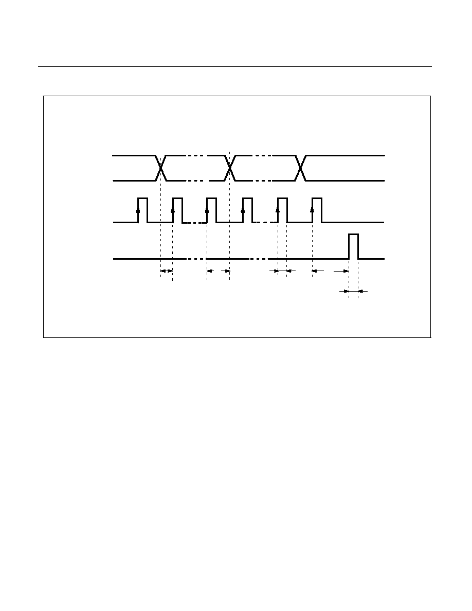
SERIAL DATA INPUT TIMING
N9
N8
N1
A1
Data
Clock
LE
t
1
t
2
t
4
t
5
t
1
, t
2
, t
3
, t
4
, t
5
1
µ
s
t
3
A5
A2
(MSB)
(LSB)
Note: On rising edge of the clock shifts one bit of the data into the shift register.
When LE is high, the data stored the shift register is transferred into the latch.