1
FUJITSU SEMICONDUCTOR
DATA SHEET
DS04213483E
ASSP
Single Serial Input
PLL Frequency Synthesizer
On-Chip prescaler
MB15C02
s
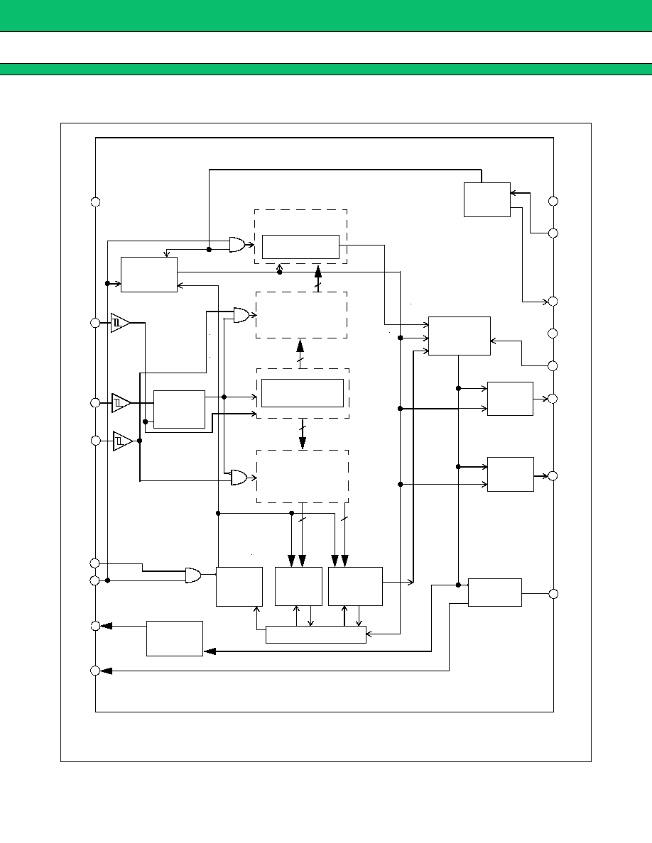
DESCRIPTION
The Fujitsu MB15C02 is a serial input Phase Locked Loop (PLL) frequency synthesizer with a prescaler. A 64/65
division is available for the prescaler that enables pulse swallow operation.
This operates with a supply voltage of 1.0 V (min.).
MB15C02 is suitable for mobile communications, such as paging systems.
s
FEATURES
· High frequency operation: 220 MHz max
@V
DD
= 1.0 V to 1.5 V
330 MHz max
@V
DD
= 1.2 V to 1.5 V
450 MHz max
@V
DD
= 1.3 V to 1.5 V
· Single power supply : V
DD
= 1.0 to 1.5 V
· Power saving function
· Pulse swallow function: 64/65
· Serial input 14-bit programmable reference divider: R = 5 to 16,383
· Serial input 18-bit programmable divider consisting of:
- Binary 6-bit swallow counter: 0 to 63
- Binary 12-bit programmable counter: 5 to 4,095
· Wide operating temperature: Ta = 20 to 60
°
C
s
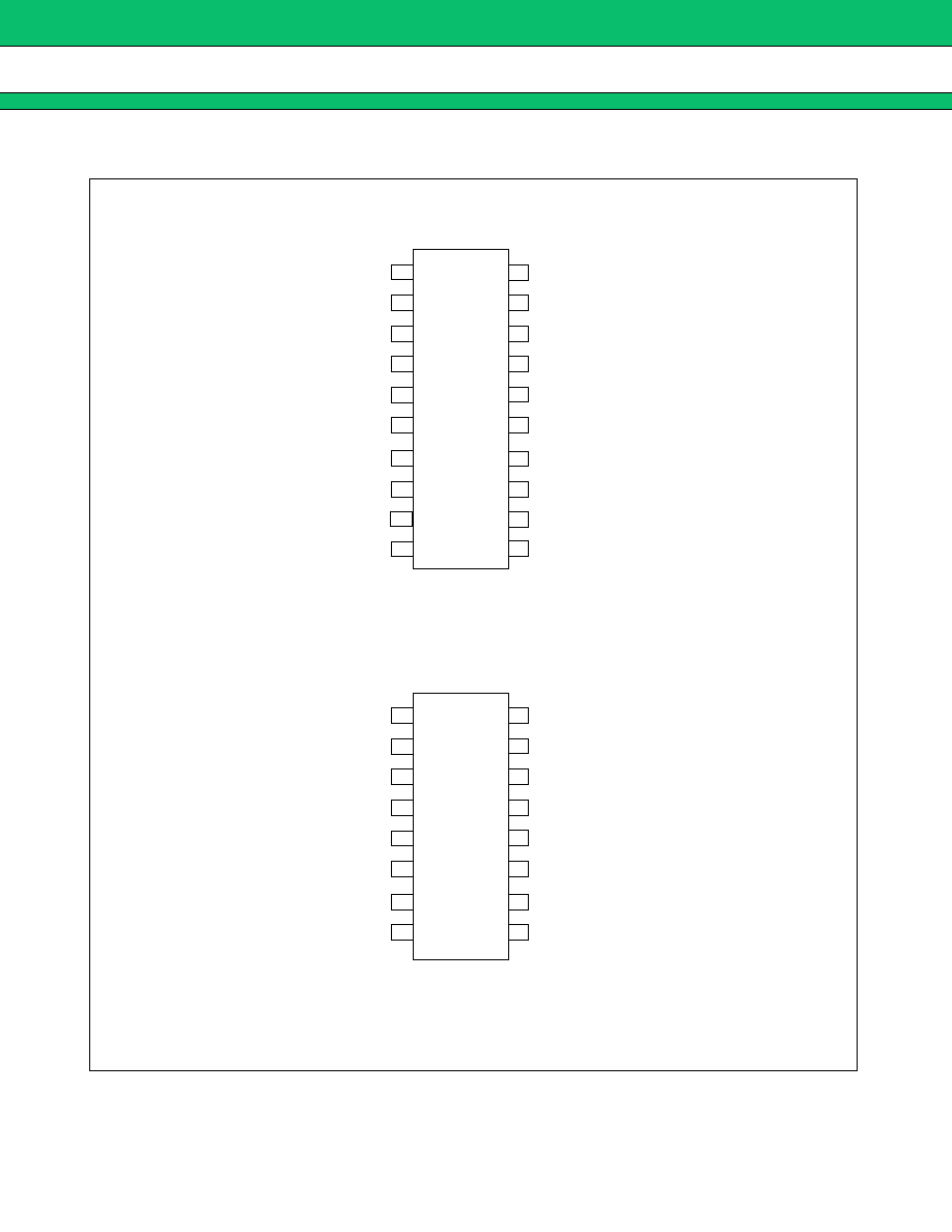
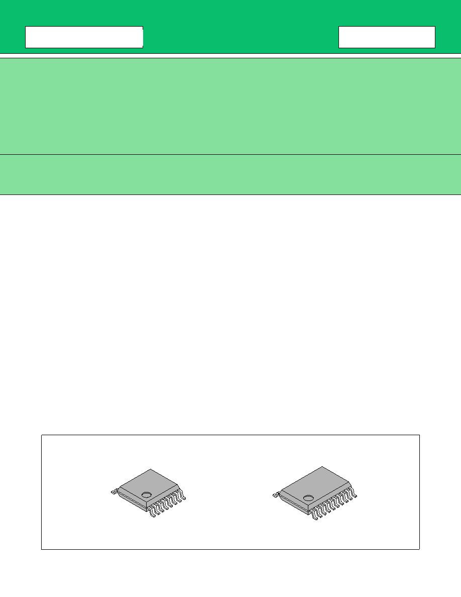
PACKAGES
16-pin, Plastic SSOP
(FPT-16P-M05)
20-pin, Plastic SSOP
(FPT-20P-M03)
3
MB15C02
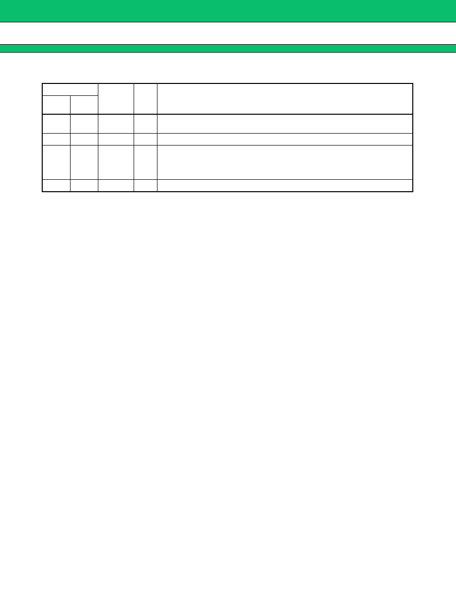
s
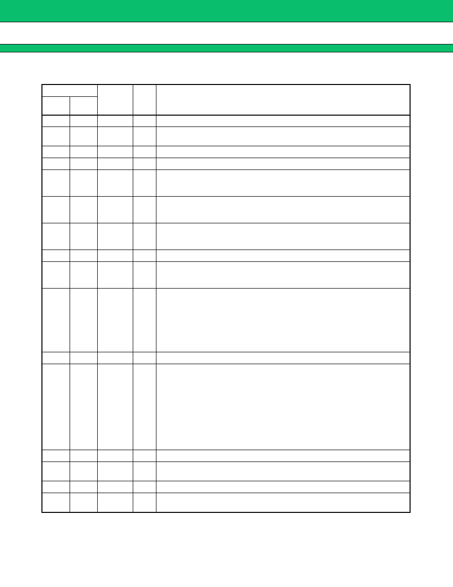
PIN DESCRIPTIONS
(Continued)
Pin no.
Pin
name
I/O
Descriptions
SSOP
16
SSOP
20
1
1
V
DD
Power supply voltage
2
2
Clock
I
Clock input for the shift register.(Schmitt trigger input)
Data is shifted into the shift register on the rising edge of the clock.
3
NC
No connection
3
4
Data
I
Serial data input using binary code.
(Schmitt trigger input)
4
5
LE
I
Load enable signal input
(Schmitt trigger input)
When LE is high, the data in the shift register is transferred to a latch,
according to the control bit in the serial data.
5
6
fin
I
Prescaler input.
A bias circuit and amplifier are at input port. Connection with an external
VCO should be done by AC coupling.
6
7
PS
I
Power saving mode control. This pin must be set at "L" at Power-ON.
PS = "H" ; Normal mode
PS = "L" ; Power saving mode
8
NC
No connection
7
9
LD
O
Lock detector signal output.
When a PLL is locking, LD outputs "H".
When a PLL is not locking, LD outputs "L".
8
10
Do
O
Charge pump output.
Phase of the charge pump can be reversed by FC input. The Do output
may be inverted by FC input. The relationships between the programmable
reference divider output (fr) and the programmable divider output (fp) are
shown below;
fr > fp :"H" level (FC = "L"), "L" level (FC = "H")
fr = fp : High impedance
fr < fp :"L" level (FC = "L"), "H" level (FC = "H")
9
11
Vp
Power supply for the charge pump.
10
12
R
O
Phase comparator output pin (for external charge pump). Relation between
the programmable reference divider output (fr) and the programmable divider
output (fp) are shown below;
When FC = "L"
fr > fp :
R = "L" level,
P = "L" level
fr = fp :
R = "L" level,
P = High impedance
fr < fp :
R = "H" level,
P = High impedance
When FC = "H"
fr > fp :
R = "H" level,
P = High impedance
fr = fp :
R = "L" level,
P = High impedance
fr < fp :
R = "L" level,
P = "L" level
13
NC
No connection
11
14
P
O
Phase comparator output pin (for external charge pump). Refer to Pin
description for
R.
P pin is a Nch open drain output.
12
15
FC
I
Phase comparator input select pin.
13
16
TEST
I
Test mode select pin.
(Pull down resistor)
Please set this pin to ground or open usually.
4
MB15C02
(Continued)
Pin no.
Pin
name
I/O
Descriptions
SSOP
16
SSOP
20
14
17
OSC
OUT
O
Oscillator output.
Connection for an external crystal.
18
NC
No connection
15
19
OSC
IN
I
Programmable reference divider input.
Oscillator input.
Clock can be input to OSC
IN
from outside. In the case, please leave OSC
OUT
pin open and make connection with OSC
IN
as AC coupling.
16
20
V
SS
Ground pin.