 | –≠–ª–µ–∫—Ç—Ä–æ–Ω–Ω—ã–π –∫–æ–º–ø–æ–Ω–µ–Ω—Ç: MB15C03 | –°–∫–∞—á–∞—Ç—å:  PDF PDF  ZIP ZIP |

DS04-21349-1E
FUJITSU SEMICONDUCTOR
DATA SHEET
ASSP
Single Serial Input
PLL Frequency Synthesizer
On-Chip prescaler
MB15C03
s
DESCRIPTION
The Fujitsu MB15C03 is a serial input Phase Locked Loop (PLL) frequency synthesizer with a prescaler. A 64/
65 division is available for the prescaler that enables pulse swallow operation.
This operates with a supply voltage of 1.0 V (min.).
MB15C03 is suitable for mobile communications, such as paging systems.
s
FEATURES
∑ Frequency operation
90 MHz @V
DD
= 1.0 to 1.5V
120 MHz @V
DD
= 1.2 to 1.5V
∑ Separate power supply : V
DD
= 1.0 to 1.5 V (for overall system)
V
P
= 2.0V to 3.5V (for a charge pump)
∑ Power saving function
∑ Pulse swallow function: 64/65
∑ Serial input 14-bit programmable reference divider: R = 5 to 16,383
∑ Serial input 18-bit programmable divider consisting of:
- Binary 6-bit swallow counter: 0 to 63
- Binary 12-bit programmable counter: 5 to 4,095
∑ Wide operating temperature: Ta = ≠20 to +60
∞
C
∑ Plastic 16-pin SSOP package (FPT-16P-M05)
s
PACKAGE
(FPT-16P-M05)
16-pin, plastic SSOP
This device contains circuitry to protect the inputs against damage due to high static voltages or electroc fields. However, it is advised that normal precautions
be taken to avoid application of any voltage higher than maximum rated voltages to this high impedance circuit.
2
MB15C03
s
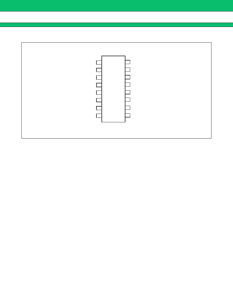
PIN ASSIGNMENT
TOP
1
2
3
4
5
6
16
15
14
13
12
11
7
8
10
9
VIEW
V
DD
V
SS
Data
LE
Clock
fin
OSC
IN
OSC
OUT
TEST
FC
LD
D
O
f
p
f
r
V
P
PS
3
MB15C03
s
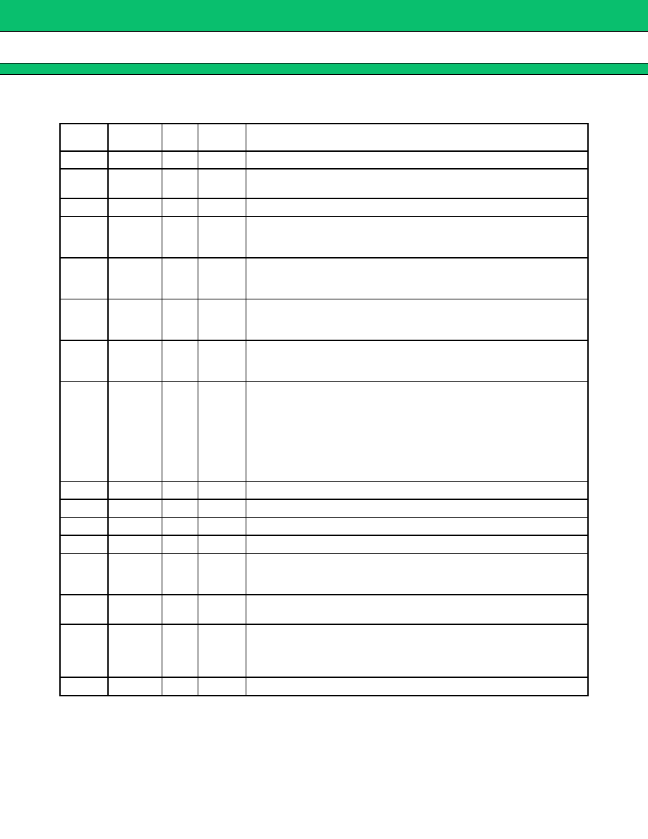
PIN DESCRIPTIONS
Pin no.
Pin
name
I/O
System
Descriptions
1
V
DD
--
1 V
Power supply voltage
2
Clock
I
1 V
Clock input for the shift register.
Data is shifted into the shift register on the rising edge of the clock.
3
Data
I
1 V
Serial data input using binary code.
4
LE
I
1 V
Load enable signal input
When LE is high, the data in the shift register is transferred to a latch,
according to the control bit in the serial data.
5
fin
I
1 V
Prescaler input.
A bias circuit and amplifier are at input port. Connection with an external
VCO should be done by AC coupling.
6
PS
I
1 V
Power saving mode control. This pin must be set at "L" at Power-ON.
PS = "H" ; Normal mode
PS = "L" ; Power saving mode
7
LD
O
1 V
Lock detector signal output.
When a PLL is locking, LD outputs "H".
When a PLL is not locking, LD outputs "L".
8
D
O
O
3 V
Charge pump output.
Phase of the charge pump can be reversed by FC input. The D
O
output
may be inverted by FC input. The relationships between the programm-
able reference divider output(fr) and the programmable divider output(f
p
)
are shown below;
f
r
> f
p
: "H" level (FC= "L"), "L" level (FC= "H")
f
r
= f
p
: High impedance
f
r
< f
p
: "L" level (FC= "L"), "H" level (FC= "H")
9
V
P
--
3 V
Power supply for the charge pump.
10
f
r
O
1 V
Programmable reference counter output (f
r
) monitoring pin.
11
f
p
O
1 V
Programmable counter output (f
p
) monitoring pin.
12
FC
I
1 V
Phase comparator input select pin.
13
TEST
I
1 V
Test mode select pin. (Pull down resistor)
Setting this pin to "H", test mode becomes available. Please set this pin
to ground or open usually.
14
OSC
OUT
O
1 V
Oscillator output.
Connection for an external crystal.
15
OSC
IN
I
1 V
Programmable reference divider input.
Oscillator input.
Clock can be input to OSC
IN
from outside. In the case, please leave
OSC
OUT
pin open and make connection with OSC
IN
as AC coupling.
16
V
SS
--
--
Ground.
4
MB15C03
s
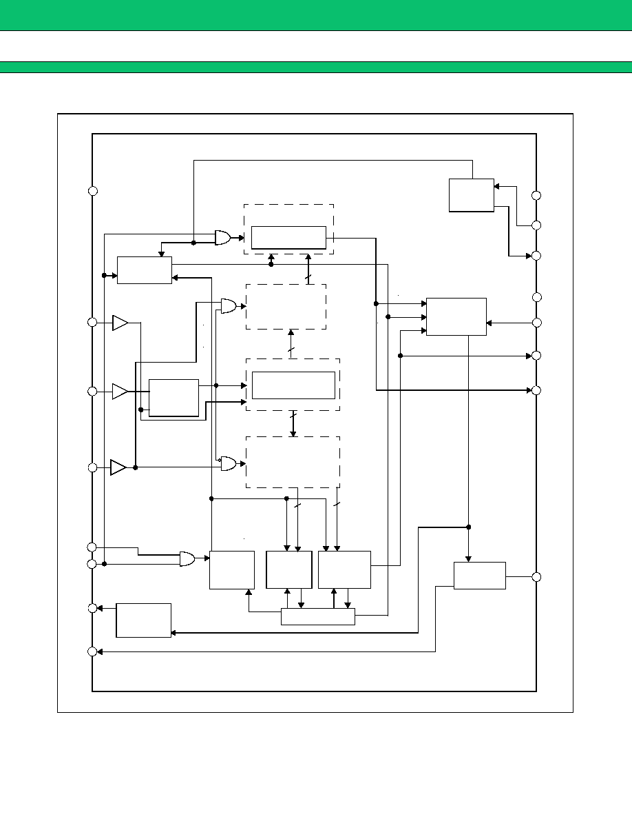
BLOCK DIAGRAM
OSC
IN
OSC
OUT
V
P
Do
Crystal
Oscillator
circuit
14-bit latch
Programmable
reference divider
Binary 14-bit
reference counter
Phase
comparator
Data
18-bit shift register
18-bit latch
Binary 6-bit
swallow
counter
Binary 12-bit
programma-
ble counter
15
14
9
8
LD
7
fin
5
Clock
4
3
LE
12
TEST
V
SS
16
Prescaler
Charge
pump
f
p
f
r
Intermittent
mode control
circuit
PS
6
FC
11
Control Circuit
13
Lock detector
f
p
f
r
10
Control
register
14
14
18
6
12
f
p
f
r
V
DD
1
2
5
MB15C03
s
ABSOLUTE MAXIMUM RATINGS
WARNING: Semiconductor devices can be permanently damaged by application of stress (voltage, current,
temperature, etc.) in excess of absolute maximum ratings. Do not exceed these ratings.
s
RECOMMENDED OPERATING CONDITIONS
WARNING: Recommended operating conditions are normal operating ranges for the semiconductor device. All
the device's electrical characteristics are warranted when operated within these ranges.
Always use semiconductor devices within the recommended operating conditions. Operation outside
these ranges may adversely affect reliability and could result in device failure.
No warranty is made with respect to uses, operating conditions, or combinations not represented on
the data sheet. Users considering application outside the listed conditions are advised to contact their
FUJITSU representative beforehand.
HandIing Precautions
∑ This device should be transported and stores in anti-static containers.
∑ This is a static-sensitive device; take proper anti-ESD precautions. Ensure that personnel and equipment are
properly grounded. Cover workbenches with grounded conductive mats.
∑ Always turn the power supply off before inserting or removing the device from its socket.
∑ Protect leads with a conductive sheet when handling or transporting PC boards with devices.
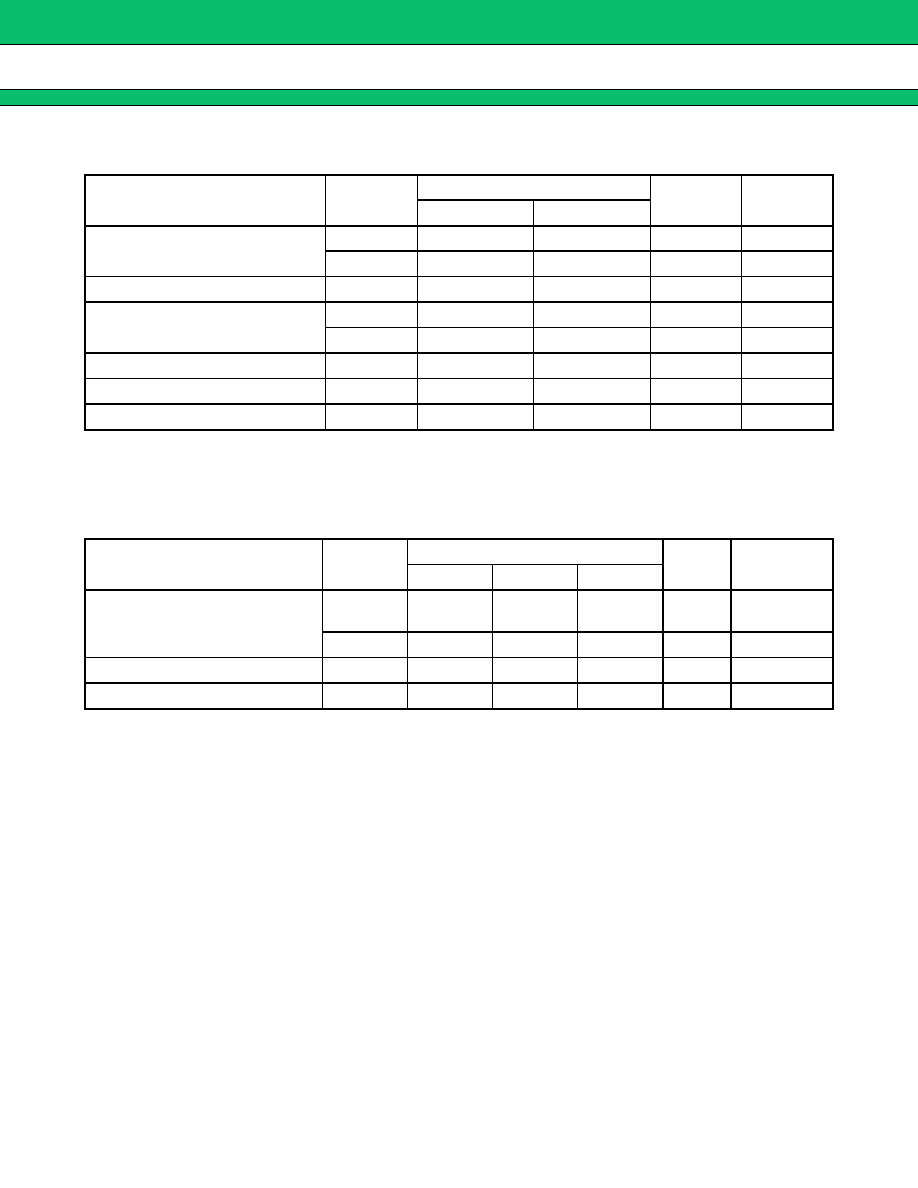
Parameter
Symbol
Rating
Unit
Remark
Min.
Max.
Power supply voltage
V
DD
GND ≠0.5
+2.0
V
V
P
GND ≠0.5
+5.0
V
Input voltage
V
IN
GND ≠0.5
V
DD
+0.5
V
Output voltage
V
OUT
GND ≠0.5
V
DD
+0.5
V
V
OUTP
GND ≠0.5
V
P
+0.5
V
Output current
I
OUT
≠10
+10
mA
Operating temperature
Ta
≠20
+60
∞
C
Storage temperature
T
stg
≠40
+125
∞
C
Parameter
Symbol
Value
Unit
Remark
Min.
Typ.
Max.
Power supply voltage
V
DD
1.0
1.2
--
--
1.5
1.5
V
For 90 MHz
For 120 MHz
V
P
2.0
--
3.5
V
Input voltage
V
IN
GND
--
V
DD
V
Operating temperature
Ta
≠20
--
+60
∞
C