 | –≠–ª–µ–∫—Ç—Ä–æ–Ω–Ω—ã–π –∫–æ–º–ø–æ–Ω–µ–Ω—Ç: MB15E03L | –°–∫–∞—á–∞—Ç—å:  PDF PDF  ZIP ZIP |
DS04-21352-1E
FUJITSU SEMICONDUCTOR
DATA SHEET
ASSP
Single Serial Input
PLL Frequency Synthesizer
On-Chip 1.2 GHz Prescaler
MB15E03L
s
DESCRIPTION
The Fujitsu MB15E03L is serial input Phase Locked Loop (PLL) frequency synthesizer with a 1.2 GHz prescaler.
A 64/65 or a 128/129 can be selected for the prescaler that enables pulse swallow operation.
The latest BiCMOS process technology is used, resuItantly a supply current is limited as low as 2.5 mA typ.
This operates with a supply voltage of 3.0 V (typ.)
Furthermore, a super charger circuit is included to get a fast tuning as well as low noise performance. As a result
of this, MB15E03L is ideally suitable for digital mobile communications, such as GSM(Global System for Mobile
Communications), PDC(800MHz)(Personal Digital Cellular).
s
FEATURES
∑ High frequency operation: 1.2 GHz max
∑ Low power supply voltage: V
CC
= 2.7 to 3.6 V
∑ Very Low power supply current : I
CC
= 2.5 mA typ. (V
CC
= 3 V)
∑ Power saving function : I
PS
= 0.1
µ
A typ.
∑ Pulse swallow function: 64/65 or 128/129
∑ Serial input 14-bit programmable reference divider: R = 5 to 16,383
∑ Serial input 18-bit programmable divider consisting of:
- Binary 7-bit swallow counter: 0 to 127
- Binary 11-bit programmable counter: 5 to 2,047
∑ Wide operating temperature: Ta = ≠40 to 85
∞
C
∑ Plastic 16-pin SSOP package (FPT-16P-M05) and 16-pin BCC package (LCC-16P-M02)
s
PACKAGES
This device contains circuitry to protect the inputs against damage due to high static voltages or electroc fields. However, it is advised that normal precautions
be taken to avoid application of any voltage higher than maximum rated voltages to this high impedance circuit.
16-pin, Plastic SSOP
(FPT-16P-M05)
(LCC-16P-M02)
16-pin, Plastic BCC

2
MB15E03L
s
PIN ASSIGNMENTS
TOP
1
2
3
4
5
6
16
15
14
13
12
11
7
8
10
9
VIEW
OSCin
R
Vp
Vcc
OSCout
Do
P
LD/fout
ZC
PS
Xfin
fin
LE
Data
Clock
GND
SSOP-16 pin
BCC-16 pin
14
13
12
11
10
9
P
LD/fout
ZC
PS
LE
Data
1
2
3
4
5
6
OSCout
V
CC
Do
GND
Xfin
V
P
7
8
16
15
fin
Clock
OSCin
R
TOP
VIEW
(FPT-16P-M05)
(LCC-16P-M02)
3
MB15E03L
s
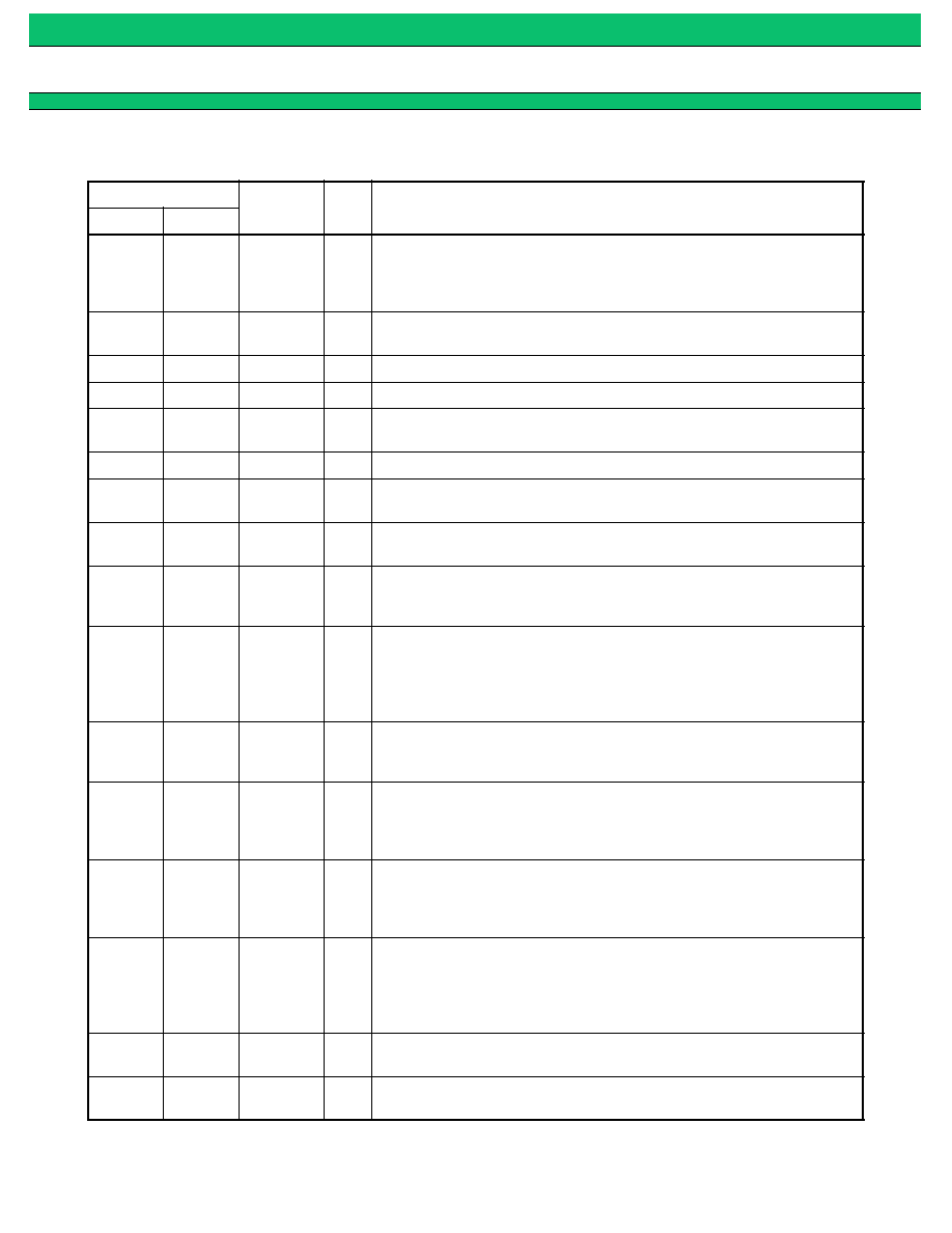
PIN DESCRIPTIONS
Pin no.
Pin
name
I/O
Descriptions
SSOP
BCC
1
16
OSC
IN
I
Programmable reference divider input.
Oscillator input.
Connection for an crystal or a TCXO.
TCXO should be connected with a coupling capacitor.
2
1
OSC
OUT
O
Oscillator output.
Connection for an external crystal.
3
2
V
P
≠
Power supply voltage input for the charge pump.
4
3
V
CC
≠
Power supply voltage input.
5
4
D
O
O
Charge pump output.
Phase of the charge pump can be reversed by FC bit.
6
5
GND
≠
Ground.
7
6
Xfin
I
Prescaler complementary input, and should be grounded via a
capacitor.
8
7
fin
I
Prescaler input.
Connection with an external VCO should be done with AC coupling.
9
8
Clock
I
Clock input for the 19-bit shift register.
Data is shifted into the shift register on the rising edge of the clock.
(Open is prohibited.)
10
9
Data
I
Serial data input using binary code.
The last bit of the data is a control bit.
(Open is prohibited.)
Control bit = "H" ; Data is transmitted to the programmable reference
counter.
Control bit = "L" ;
Data is transmitted to the programmable counter.
11
10
LE
I
Load enable signal input
(Open is prohibited.)
When LE is high, the data in the shift register is transferred to a latch,
according to the control bit in the serial data.
12
11
PS
I
Power saving mode control. This pin must be set at "L" at Power-ON.
(Open is prohibited.)
PS = "H" ; Normal mode
PS = "L" ; Power saving mode
13
12
ZC
I
Forced high-impedance control for the charge pump (with internal
pull up resistor.)
ZC = "H" ; Normal Do output.
ZC = "L" ; Do becomes high impedance.
14
13
LD/fout
O
Lock detect signal output(LD)/phase comparator monitoring
output (fout).
The output signal is selected by LDS bit in the serial data.
LDS = "H" ; outputs fout (fr/fp monitoring output)
LDS = "L" ; outputs LD ("H" at locking, "L" at unlocking.)
15
14
P
O
Phase comparator output for an external charge pump. Nch open
drain output.
16
15
R
O
Phase comparator output for an external charge pump. CMOS
output.
4
MB15E03L
s
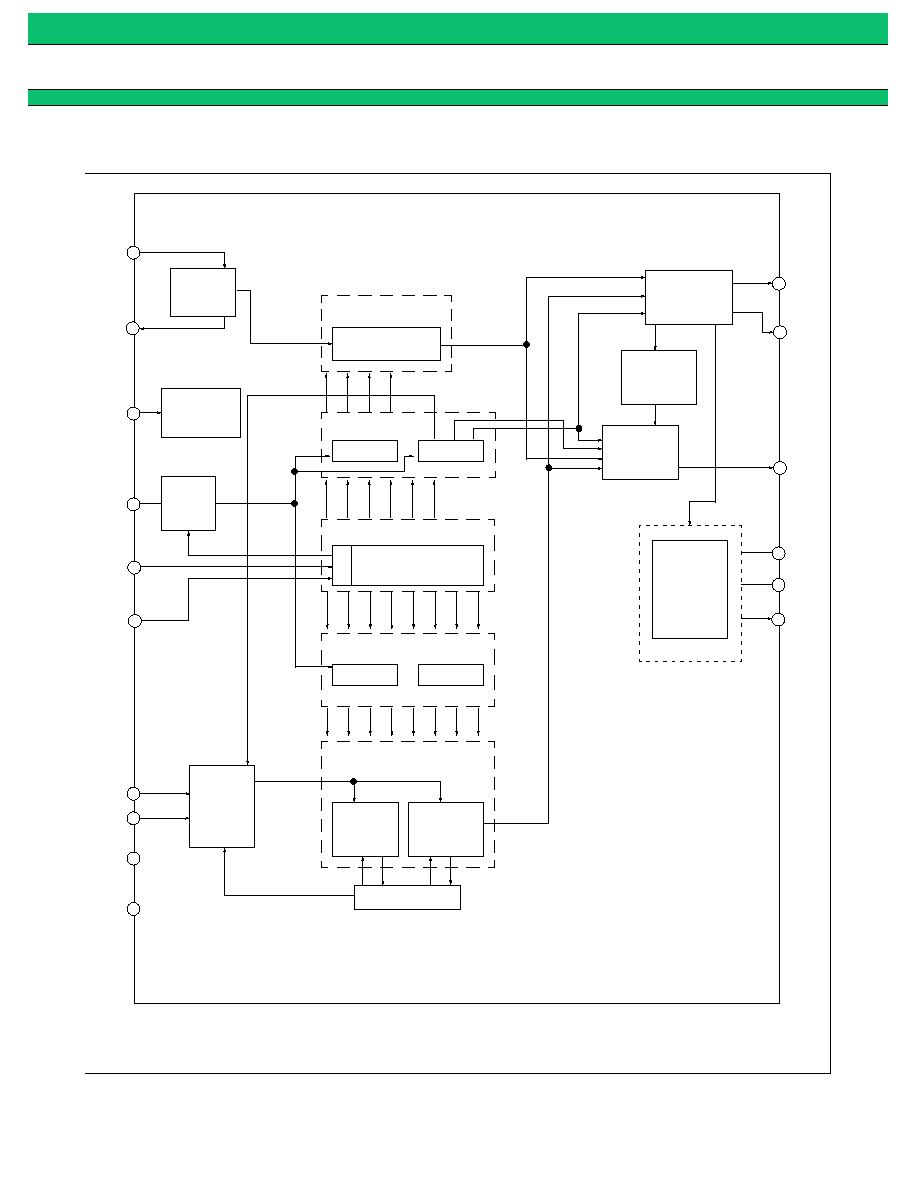
BLOCK DIAGRAM
OSC
IN
OSC
OUT
V
P
V
CC
Crystal
Oscillator
circuit
17-bit latch
Programmable
reference divider
Binary 14-bit
reference counter
Phase
comparator
LD/fout
Data
19-bit shift register
19-bit shift register
7-bit latch
18-bit latch
11-bit latch
Binary 7-bit
swallow
counter
Programmable divider
Binary 11-bit
programma-
ble counter
1
2
3
4
D
O
5
GND
6
Xf
IN
7
Clock
9
10
LE
11
PS
12
14
P
R
16
Prescaler
64/65,
128/129
Super
charger
LE
SW
MD
fp
fp
fp
fr
fr
LD/fr/fp
selector
Intermittent
mode control
(power save)
LE
f
IN
8
LD
Lock
detector
SW
C
N
T
1-bit
control
latch
14-bit latch
3-bit latch
LDS
FC
ZC
13
Control Circuit
15
Note: SSOP-16 pin
5
MB15E03L
s
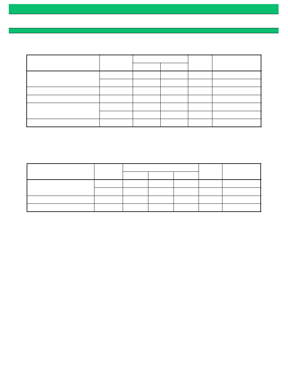
ABSOLUTE MAXIMUM RATINGS
WARNING: Semiconductor devices can be permanently damaged by application of stress (voltage, current,
temperature, etc.) in excess of absolute maximum ratings. Do not exceed these ratings.
s
RECOMMENDED OPERATING CONDITIONS
WARNING: Recommended operating conditions are normal operating ranges for the semiconductor device. All
the device's electrical characteristics are warranted when operated within these ranges.
Always yse semiconductor devices within the recommended operating conditions. Operation outside
these ranges may adversely affect reliability and could result in device failure.
No warranty is made with repect to uses, operating conditions, or combinations not represented on
the data sheet. Users considering application outside the listed conditions are advised to contact their
FUJITSU representative beforehand.
Handling Precautions
∑ This device should be transported and stored in anti-static containers.
∑ This is a static-sensitive device; take proper anti-ESD precautions. Ensure that personnel and equipment are
properly grounded. Cover workerbenches with grounded conductive mats.
∑ Always turn the power supply off before inserting or removing the device from its socket.
∑ Protect leads with a conductive sheet when handling or transporting PC boards with devices.
Parameter
Symbol
Rating
Unit
Remark
Min.
Max.
Power supply voltage
V
CC
≠0.5
+4.0
V
V
P
V
CC
+6.0
V
Input voltage
V
I
≠0.5
V
CC
+0.5
V
Output voltage
V
O
≠0.5
V
CC
+0.5
V
Output current
I
O
≠10
+10
mA
Except D
O
output
I
Od
≠25
+25
mA
D
O
output
Storage temperature
T
stg
≠55
+125
∞
C
Parameter
Symbol
Value
Unit
Remark
Min.
Typ.
Max.
Power supply voltage
V
CC
2.7
3.0
3.6
V
V
P
V
CC
≠
6.0
V
Input voltage
V
I
GND
≠
V
CC
V
Operating temperature
Ta
≠40
≠
+85
∞
C