DS04-21343-1E
FUJITSU SEMICONDUCTOR
DATA SHEET
ASSP
Single Serial Input
PLL Frequency Synthesizer
On-Chip 2.5 GHz Prescaler
MB15E07
s
DESCRIPTION
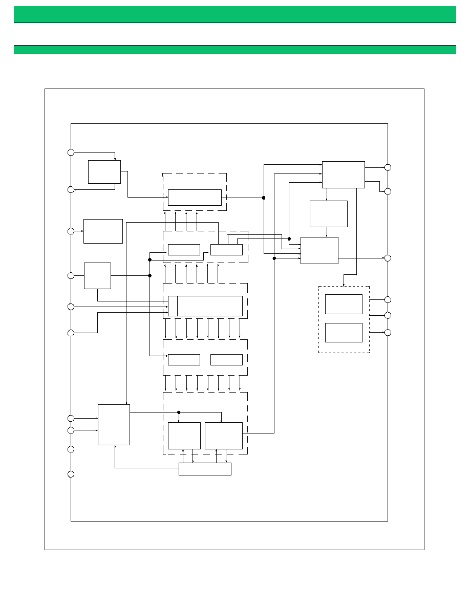
The Fujitsu MB15E07 is serial input Phase Locked Loop (PLL) frequency synthesizer with a 2.5 GHz prescaler.
A 32/33 or a 64/65 can be selected for the prescaler that enables pulse swallow operation.
The latest BiCMOS process technology is used, resuItantly a supply current is limited as low as 8 mA typ. This
operates with a supply voltage of 3.0 V (typ.)
Furthermore, a super charger circuit is included to get a fast tuning as well as low noise performance. As a result
of this, MB15E07 is ideally suitable for digital mobile communications, such as GSM (Global System for Mobile
Communications).
s
FEATURES
∑ High frequency operation: 2.5 GHz max (@ P= 64/65)
1.8 GHz max (@P = 32/33)
∑ Low power supply voltage: V
CC
= 2.7 to 3.6 V
∑ Very Low power supply current : I
CC
= 8.0 mA typ. (V
CC
= 3 V)
∑ Power saving function : I
PS
= 0.1
µ
A typ.
∑ Pulse swallow function: 32/33 or 64/65
∑ Serial input 14-bit programmable reference divider: R = 5 to 16,383
∑ Serial input 18-bit programmable divider consisting of:
- Binary 7-bit swallow counter: 0 to 127
- Binary 11-bit programmable counter: 5 to 2,047
∑ Wide operating temperature: Ta = ≠40 to 85
∞
C
∑ Plastic 16-pin SSOP package (FPT-16P-M05)
s
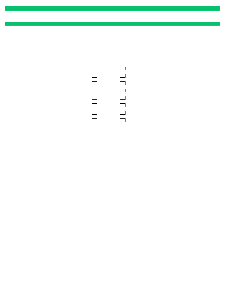
PACKAGE
16-pin, Plastic SSOP
(FPT-16P-M05)
3
MB15E07
s
PIN DESCRIPTIONS
Pin no.
Pin name
I/O
Descriptions
1
OSC
IN
I
Programmable reference divider input.
Oscillator input.
Connection for an crystal or a TCXO.
TCXO should be connected with a coupling capacitor.
2
OSC
OUT
O
Oscillator output.
Connection for an external crystal.
3
V
P
≠
Power supply voltage input for the charge pump.
4
V
CC
≠
Power supply voltage input.
5
D
O
O
Charge pump output.
Phase of the charge pump can be reversed by FC bit.
6
GND
≠
Ground.
7
Xfin
I
Prescaler complementary input, and should be grounded via a capacitor.
8
fin
I
Prescaler input.
Connection with an external VCO should be done with AC coupling.
9
Clock
I
Clock input for the 19-bit shift register.
Data is shifted into the shift register on the rising edge of the clock.
(Open
is prohibited.)
10
Data
I
Serial data input using binary code.
The last bit of the data is a control bit.
(Open is prohibited.)
Control bit = "H" ;Data is transmitted to the programmable reference
counter.
Control bit = "L" ;Data is transmitted to the programmable counter.
11
LE
I
Load enable signal input
(Open is prohibited.)
When LE is high, the data in the shift register is transferred to a latch,
according to the control bit in the serial data.
12
PS
I
Power saving mode control. This pin must be set at "L" at Power-ON.
(Open is prohibited.)
PS = "H" ; Normal mode
PS = "L" ; Power saving mode
13
ZC
I
Forced high-impedance control for the charge pump (with internal pull up
resistor.)
ZC = "H" ; Normal Do output.
ZC = "L" ; Do becomes high impedance.
14
LD/fout
O
Lock detect signal output(LD)/phase comparator monitoring
output (fout).
The output signal is selected by LDS bit in the serial data.
LDS = "H" ; outputs fout (fr/fp monitoring output)
LDS = "L" ; outputs LD ("H" at locking, "L" at unlocking.)
15
P
O
Phase comparator output for an external charge pump. Nch open drain
output.
16
R
O
Phase comparator output for an external charge pump. CMOS output.

5
MB15E07
s
ABSOLUTE MAXIMUM RATINGS
Note: Permanent device damage may occur if the above
Absolute Maximum Ratings
are exceeded. Functional
operation should be restricted to the conditions as detailed in the operational sections of this data sheet.
Exposure to absolute maximum rating conditions for extended periods may affect device reliability.
s
RECOMMENDED OPERATING CONDITIONS
Handling Precautions
∑ This device should be transported and stores in anti-static containers.
∑ This is a static-sensitive device; take proper anti-ESD precautions. Ensure that personnel and equipment are
properly grounded. Cover workbenches with grounded conductive mats.
∑ Always turn the power supply off before inserting or removing the device from its socket.
∑ Protect leads with a conductive sheet when handling or transporting PC boards with devices.
Parameter
Symbol
Rating
Unit
Remark
Power supply voltage
V
CC
≠0.5 to +4.0
V
V
P
V
CC
to +6.0
V
Input voltage
V
I
≠0.5 to V
CC
+0.5
V
Output voltage
V
O
≠0.5 to V
CC
+0.5
V
Storage temperature
T
stg
≠55 to +125
∞
C
Parameter
Symbol
Value
Unit
Remark
Min.
Typ.
Max.
Power supply voltage
V
CC
2.7
3.0
3.6
V
V
P
V
CC
≠
6.0
V
Input voltage
V
I
GND
≠
V
CC
V
Operating temperature
Ta
≠40
≠
+85
∞
C