DS04-21371-1E
FUJITSU SEMICONDUCTOR
DATA SHEET
ASSP
Fractional-N
PLL Frequency
Synthesizer
MB15F83UL
s
s
s
s
DESCRIPTION
The Fujitsu MB15F83UL is Fractional-N Phase Locked Loop (PLL) frequency synthesizer with fast lock up function.
The Fractional-N PLL operating up to 2000 MHz and the integer PLL operating up to 600 MHz are integrated on
one chip.
The MB15F83UL is used, as charge pump which is well-balanced output current with 1.5 mA and 6 mA selectable
by serial data, direct power save control and digital lock detector. In addition, the MB15F83UL adopts a new
architecture to achieve fast lock.
The new package (Thin Bump Chip Carrier20) decreases a mount area of MB15F83UL more than 30
%
comparing
with the former B.C.C.16 (for dual PLL, MB15F03SL) .
The MB15F83UL is ideally suited for wireless mobile communications, such as GSM.
s
s
s
s
FEATURES
∑ High frequency operation
: RF synthesizer : 2000 MHz Max.
: IF synthesizer : 600 MHz Max.
∑ Low power supply voltage
: V
CC
=
2.7 V to 3.6 V
∑ Ultra Low power supply current
: I
CC
=
5.8 mA Typ. (V
CC
=
Vp
=
3.0 V, Ta
=
+
25
∞
C, SW
=
0 in IF and RF locking
state)
(Continued)
s
s
s
s
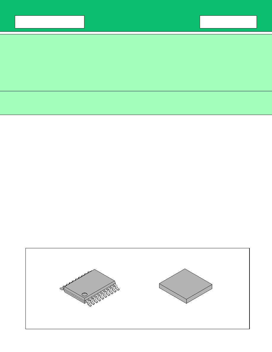
PACKAGES
20-pin, Plastic TSSOP
20-pad, Plastic BCC
(FPT-20P-M06)
(LCC-20P-M05)
MB15F83UL
2
(Continued)
∑ Direct power saving function : Power supply current in power saving mode
Typ. 0.1
µ
A (V
CC
=
Vp
=
3.0 V, Ta
=
+
25
∞
C) , Max. 10
µ
A (V
CC
=
Vp
=
3.0 V)
∑ Fractional function : modulo 13 fixed (implemented in RF-PLL)
∑ Dual modulus prescaler : 2000 MHz prescaler (16/17 fixed) /600 MHz prescaler (8/9 or 16/17)
∑ Serial input programmable reference divider : RF : 7 bit (3 to 127) /IF : 14 bit (3 to 16383)
∑ Serial input programmable divider consisting of :
RF section - Binary 4-bit swallow counter : 0 to 15
- Binary 10-bit programmable counter : 18 to 1,023
- Binary 4-bit fractional counter numerator : 0 to 15
IF section - Binary 4-bit swallow counter : 0 to 15
- Binary 11-bit programmable counter : 3 to 2,047
∑ On-chip phase comparator for fast lock and low noise
∑ Operating temperature : Ta
=
-
40
∞
C to
+
85
∞
C
∑ Small package Bump Chip Carrier.0 (3.4 mm
◊
3.6 mm
◊
0.6 mm)
s
s
s
s
PIN ASSIGNMENTS
(BCC-20)
TOP VIEW
(LCC-20P-M05)
GND
Clock
D
OIF
1
2
3
4
5
6
7
8
9 10 11
12
13
14
15
16
19 18 17
20
GND
IF
GND
RF
V
CCIF
Vp
IF
LE
fin
RF
fin
IF
V
CCRF
PS
RF
PS
IF
Xfin
RF
Xfin
IF
OSC
IN
Data
LD/fout
D
ORF
Vp
RF
(TSSOP-20)
TOP VIEW
(FPT-20P-M06)
OSC
IN
GND
fin
IF
Xfin
IF
GND
IF
V
CCIF
PS
IF
Vp
IF
D
OIF
LD/fout
Clock
Data
LE
fin
RF
Xfin
RF
GND
RF
V
CCRF
PS
RF
Vp
RF
D
ORF
1
2
3
4
5
6
7
8
9
10
20
19
18
17
16
15
14
13
12
11
MB15F83UL
3
s
s
s
s
PIN DESCRIPTION
Pin no.
Pin
name
I/O
Descriptions
TSSOP
BCC
1
19
OSC
IN
I
The programmable reference divider input pin. TCXO should be connected with
an AC coupling capacitor.
2
20
GND
Ground pin for OSC input buffer and the shift register circuit.
3
1
fin
IF
I
Prescaler input pin for the IF-PLL.
Connection to an external VCO should be AC coupling.
4
2
Xfin
IF
I
Prescaler complimentary input pin for the IF-PLL section.
This pin should be grounded via a capacitor.
5
3
GND
IF
Ground pin for the IF-PLL section.
6
4
V
CCIF
Power supply voltage input pin for the IF-PLL section (except for the charge
pump circuit) , the shift register and the oscillator input buffer.
When power is OFF, latched data of IF-PLL is lost.
7
5
PS
IF
I
Power saving mode control signal pin for the IF-PLL section. This pin must be set
at "L" when the power supply is started up. (Open is prohibited.)
PS
IF
=
"H"; Normal mode / PS
IF
=
"L"; Power saving mode
8
6
Vp
IF
Power supply voltage input pin for the IF-PLL charge pump.
9
7
Do
IF
O
Charge pump output pin for the IF-PLL section.
Phase characteristics of the phase detector can be reversed by FC-bit.
10
8
LD/fout O
Look detect signal output (LD) /phase comparator monitoring output (fout) pins.
The output signal is selected by an LDS bit in a serial data.
LDS bit
=
"H"; outputs fout signal / LDS bit
=
"L"; outputs LD signal
11
9
Do
RF
O
Charge pump output pin for the RF-PLL section.
Phase characteristics of the phase detector can be reversed by FC-bit.
12
10
Vp
RF
Power supply voltage input pin for the RF-PLL charge pump.
13
11
PS
RF
I
Power saving mode control pin for the RF-PLL section. This pin must be set at
"L" when the power supply is started up. (Open is prohibited. )
PS
RF
=
"H"; Normal mode / PS
RF
=
"L"; Power saving mode
14
12
V
CCRF
Power supply voltage input pin for the RF-PLL section (except for the charge
pump circuit) .
15
13
GND
RF
Ground pin for the RF-PLL section.
16
14
Xfin
RF
I
Prescaler complimentary input pin for the RF-PLL section.
This pin should be grounded via a capacitor.
17
15
fin
RF
I
Prescaler input pin for the RF-PLL.
Connection to an external VCO should be AC coupling.
18
16
LE
I
Load enable signal input pin (with the schmitt trigger circuit.)
On a rising edge of load enable, data in the shift register is transferred to the cor-
responding latch according to the control bit in a serial data.
19
17
Data
I
Serial data input pin (with the schmitt trigger circuit.)
A data is transferred to the corresponding latch (IF-ref counter, IF-prog. counter,
RF-ref. counter, RF-prog. counter) according to the control bit in a serial data.
20
18
Clock
I
Clock input pin for the 23-bit shift register (with the schmitt trigger circuit.)
One bit data is shifted into the shift register on a rising edge of the clock.
MB15F83UL
4
s
s
s
s
BLOCK DIAGRAM
7
3
4
1
17
11
10
16
13
18
19
20
12
15
14
2
9
8
5
6
PS
IF
fin
IF
Xfin
IF
OSC
IN
(5)
(7)
(8)
(9)
(18)
(17)
(16)
(11)
(14)
(15)
(1)
(2)
(19)
Power
saving
IF-PLL
Prescaler
(IF-PLL)
8/9, 16/17
4-bit latch
11-bit latch
Binary 14-bit pro-
grammable ref.
counter (IF-PLL)
Binary 11-bit
programmable
counter
(IF-PLL)
VCC
IF
GND
IF
Vp
IF
(4)
(3)
(6)
(10)
(13)
(12)
(20)
fp
IF
Phase
comp.
(IF-PLL)
Charge
pump
(IF-PLL)
Do
IF
LD/fout
14-bit latch
Binary 4-bit
swallow counter
(IF-PLL)
LDS
T1
T2
SWC
FCC
CSC
6-bit latch
Lock
Det.
(IF-PLL)
LD
IF
Slector
LD
IF
LD
RF
fr
IF
fr
RF
fp
IF
fp
RF
OR
Lock
Det.
(RF-PLL)
Phase
comp.
(RF-PLL)
Charge
pump
(RF-PLL)
Do
RF
SC
(RF-PLL)
SC1
SC2
Vp
RF
GND
RF
GND
Vcc
RF
Clock
Data
LE
PS
RF
Xfin
RF
fin
RF
Schmitt
circuit
Schmitt
circuit
Schmitt
circuit
C
N
1
C
N
2
C
N
3
23-bit shift
register
Latch selector
Power
saving
RF-PLL
Prescaler
(RF-PLL)
16/17
MD2
Binary 4-bit
swallow counter
(RF-PLL)
Binary 10-bit
programmable
counter
(RF-PLL)
4-bit latch
10-bit latch
MD1
F
1
F
2
F
3
F
4
4-bit latch
Fractional
Counter
13
fr
RF
fp
RF
fr
RF
fp
RF
Selector
SC1
SC2
SFW
FCF
CSF
5-bit latch
7-bit latch
Binary 7-bit pro-
grammable ref.
counter
(RF-PLL)
OR
O : TSSOP 20
( ) : BCC 20
MB15F83UL
5
s
s
s
s
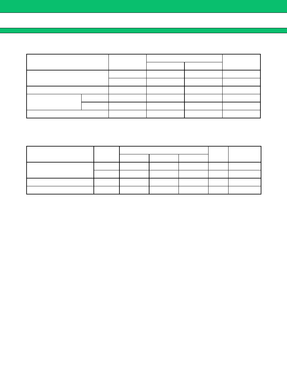
ABSOLUTE MAXIMUM RATINGS
WARNING: Semiconductor devices can be permanently damaged by application of stress (voltage, current,
temperature, etc.) in excess of absolute maximum ratings. Do not exceed these ratings.
s
s
s
s
RECOMMENDED OPERATING CONDITIONS
WARNING: The recommended operating conditions are required in order to ensure the normal operation of the
semiconductor device. All of the device's electrical characteristics are warranted when the device is
operated within these ranges.
Always use semiconductor devices within their recommended operating condition ranges. Operation
outside these ranges may adversely affect reliability and could result in device failure.
No warranty is made with respect to uses, operating conditions, or combinations not represented on
the data sheet. Users considering application outside the listed conditions are advised to contact their
FUJITSU representatives beforehand.
Parameter
Symbol
Rating
Unit
Min.
Max.
Power supply voltage
V
CC
-
0.5
+
4.0
V
Vp
V
CC
+
4.0
V
Input voltage
V
I
-
0.5
V
CC
+
0.5
V
Output voltage
LD / fout
V
O
GND
V
CC
V
Do
V
DO
GND
Vp
V
Storage temperature
Tstg
-
55
+
125
∞
C
Parameter
Symbol
Value
Unit
Remark
Min.
Typ.
Max.
Power supply voltage
V
CC
2.7
3.0
3.6
V
V
CCRF
=
V
CCIF
Vp
V
CC
3.0
3.6
V
Input voltage
V
I
GND
V
CC
V
Operating temperature
Ta
-
40
+
85
∞
C