 | –≠–ª–µ–∫—Ç—Ä–æ–Ω–Ω—ã–π –∫–æ–º–ø–æ–Ω–µ–Ω—Ç: MB3759C | –°–∫–∞—á–∞—Ç—å:  PDF PDF  ZIP ZIP |

DS04-27200-6E
FUJITSU SEMICONDUCTOR
DATA SHEET
ASSP For Power Management Applications
BIPOLAR
Switching Regulator Controller
(Switchable between push-pull and single-end functions)
MB3759
s
s
s
s
DESCRIPTION
The MB3759 is a control IC for constant-frequency pulse width modulated switching regulators.
The IC contains most of the functions required for switching regulator control circuits. This reduces both the
component count and assembly work.
s
s
s
s
FEATURES
∑ Drives a 200 mA load
∑ Can be set to push-pull or single-end operation
∑ Prevents double pulses
∑ Adjustable dead-time
∑ Error amplifier has wide common phase input range
∑ Built in a circuit to prevent misoperation due to low power supply voltage.
∑ Built in an internal 5 V reference voltage with superior voltage reduction characteristics
s
s
s
s
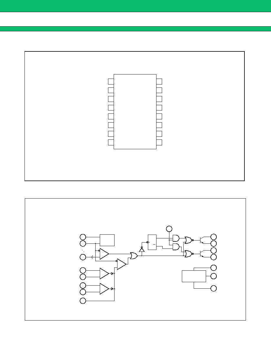
PACKAGES
16-pin plastic DIP
16-pin ceramic DIP
16-pin plastic SOP
(DIP-16P-M04)
(DIP-16C-C01)
(FPT-16P-M06)
MB3759
2
s
s
s
s
PIN ASSIGNMENT
s
s
s
s
BLOCK DIAGRAM
(TOP VIEW)
(
DIP-16P-M04
)
(
DIP-16C-C01
)
(
FPT-16P-M06
)
+
IN1
-
IN1
FB
DT
C
T
R
T
GND
C
1
1
2
3
4
5
6
7
8
16
15
14
13
12
11
10
9
+
IN2
-
IN2
V
REF
OC
V
CC
C
2
E
2
E
1
0.2 V
+
+
-
-
A
1
A
2
T
OSC
R
T
+
IN1
6
+
IN2
-
IN1
-
IN2
C
T
5
4
2
16
15
3
Q
Q
8
9
11
12
14
7
10
C
1
E
1
C
2
E
2
V
CC
V
REF
GND
13
1
DT
FB
=
Dead time
control
Reference
regurator
PMW comparator
Error amp.1
Error amp.2
Feed back
Output
control
OC
MB3759
3
s
s
s
s
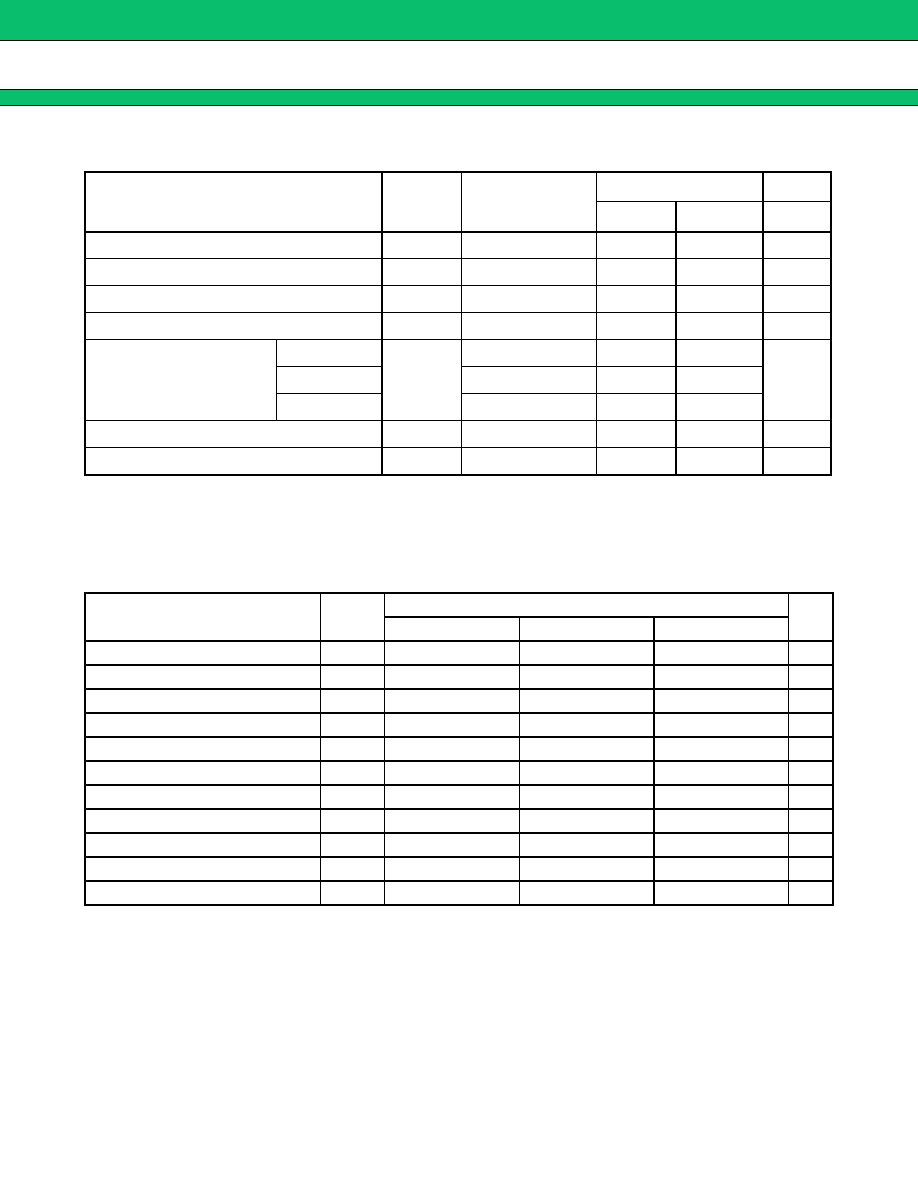
ABSOLUTE MAXIMUM RATINGS
*: When mounted on a 4 cm square double-sided epoxy circuit board (1.5 mm thickness)
The ceramic circuit board is 3 cm x 4 cm (0.5 mm thickness)
WARNING: Semiconductor devices can be permanently damaged by application of stress (voltage, current,
temperature, etc.) in excess of absolute maximum ratings. Do not exceed these ratings.
s
s
s
s
RECOMMENDED OPERATING CONDITIONS
Note: Values are for standard derating conditions. Give consideration to the ambient temperature and power con-
sumption if using a high supply voltage.
WARNING: The recommended operating conditions are required in order to ensure the normal operation of the
semiconductor device. All of the device's electrical characteristics are warranted when the device is
operated within these ranges.
Always use semiconductor devices within their recommended operating condition ranges. Operation
outside these ranges may adversely affect reliability and could result in device failure.
No warranty is made with respect to uses, operating conditions, or combinations not represented on
the data sheet. Users considering application outside the listed conditions are advised to contact their
FUJITSU representatives beforehand.
Parameter
Symbol
Condition
Rating
Unit
Min
Max
Power supply voltage
V
CC
--
--
41
V
Collector output voltage
V
CE
--
--
41
V
Collector output current
I
CE
--
--
250
mA
Amplifier input voltage
V
I
--
--
V
CC
+
0.3
V
Power dissipation
Plastic DIP
P
D
Ta
+
25
∞
C
--
1000
mW
Ceramic DIP
Ta
+
60
∞
C
--
800
SOP *
Ta
+
25
∞
C
--
620
Operating temperature
Top
--
-
30
+
85
∞
C
Storage temperature
Tstg
--
-
55
+
125
∞
C
Parameter
Symbol
Value
Unit
Min
Typ
Max
Power supply voltage
V
CC
7
15
32
V
Collector output voltage
V
CE
--
--
40
V
Collector output current
I
CE
5
--
200
mA
Amplifier input voltage
V
IN
-
0.3
0 to V
R
V
CC
-
2
V
FB sink current
I
SINK
--
--
0.3
mA
FB source current
I
SOURCE
--
--
2
mA
Reference section output current
I
REF
--
5
10
mA
Timing resistor
R
T
1.8
30
500
k
Timing capacitor
C
T
470
1000
10
6
pF
Oscillator frequency
fosc
1
40
300
kHz
Operating temperature
Top
-
30
+
25
+
85
∞
C

MB3759
4
s
s
s
s
ELECTRICAL CHARACTERISTICS
(Continued)
(V
CC
= 15 V, Ta = +25
∞
C)
Parameter
Symbol
Condition
Value
Unit
Min
Typ
Max
Reference
section
Output voltage
V
REF
I
O
=
1 mA
4.75
5.0
5.25
V
Input regulation
V
R(IN)
7 V
V
CC
40 V,
Ta
=
+
25
∞
C
--
2
25
mV
Load regulation
V
R(LD)
1 mA
I
O
10 mA,
Ta
=
+
25
∞
C
--
-
1
-
15
mV
Temperature stability
V
R
/
T
-
20
∞
C
Ta
+
85
∞
C
--
±
200
±
750
µ
V/
∞
C
Short circuit output
current
I
SC
--
15
40
--
mA
Reference lockout
voltage
--
--
--
4.3
--
V
Reference hysteresis
voltage
--
--
--
0.3
--
V
Oscillator
section
Oscillator frequency
fosc
R
T
=
30 k
,
C
T
=
1000 pF
36
40
44
kHz
Standard deviation
of frequency
--
R
T
=
30 k
,
C
T
=
1000 pF
--
±
3
--
%
Frequency change
with voltage
--
7 V
V
CC
40 V,
Ta
=
+
25
∞
C
--
±
0.1
--
%
Frequency change with
temperature
fosc/
T
-
20
∞
C
Ta
+
85
∞
C
--
±
0.01
±
0.03
%/
∞
C
Dead-time
control section
Input bias current
I
D
0
V
I
5.25 V
--
-
2
-
10
µ
A
Maximum duty cycle (Each
output)
--
V
I
=
0
40
45
--
%
Input
threshold
voltage
0% duty
cycle
V
DO
--
--
3.0
3.3
V
Max. duty
cycle
V
DM
--
0
--
--
V
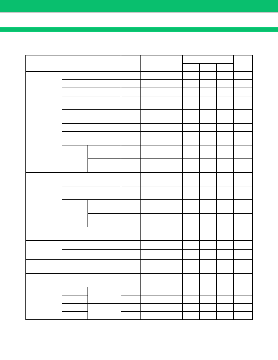
MB3759
5
(Continued)
(V
CC
= 15 V, Ta = +25
∞
C)
Parameter
Symbol
Condition
Value
Unit
Min
Typ
Max
Error
amplifier
section
Input offset voltage
V
IO
V
O (pin3)
= 2.5 V
--
±
2
±
10
mV
Input offset current
I
IO
V
O (pin3)
= 2.5 V
--
±
25
±
250
nA
Input bias current
I
I
V
O (pin3)
= 2.5 V
--
-
0.2
-
1.0
µ
A
Common-mode input
voltage
V
CM
7 V
V
CC
40 V
-
0.3
--
V
CC
-
2
V
Open-loop voltage
amplification
A
V
0.5 V
V
O
3.5 V
70
95
--
dB
Unity-gain bandwidth
BW
A
V
= 1
--
800
--
kHz
Common-mode
rejection ratio
CMR
V
CC
= 40 V
65
80
--
dB
Output sink
current
(pin 3)
ISINK
I
SINK
-5 V
V
ID
-15 mV,
V
O
= 0.7 V
0.3
0.7
--
mA
ISOURCE
I
SOURCE
15 mV
V
ID
5V,
V
O
= 3.5 V
-
2
-
10
--
mA
Output
section
Collector leakage current
I
CO
V
CE
= 40 V,
V
CC
= 40 V
--
--
100
µ
A
Emitter leakage current
I
EO
V
CC
= V
C
= 40 V,
V
E
= 0
--
--
-
100
µ
A
Collector
emitter
saturation
voltage
Emitter
grounded
V
SAT(C)
V
E
= 0, I
C
= 200 mA
--
1.1
1.3
V
Emitter
follower
V
SAT(E)
V
C
= 15 V,
I
E
=
-
200 mA
--
1.5
2.5
V
Output control input
current
I
OPC
V
I
= V
REF
--
1.3
3.5
mA
PWM
comparator
section
Input threshold voltage
V
TH
0% Duty
--
4
4.5
V
Input sink current (pin 3)
I
SINK
V
O (pin3)
= 0.7 V
0.3
0.7
--
mA
Power supply current
I
CC
V
(pin4
) = 2 V,
See Fig-2
--
8
--
mA
Standby current
I
CCQ
V
(pin6
) = V
REF
,
I/O open
--
7
12
mA
Switching
characteristics
Rise time
Emitter
grounded
t
R
R
L
= 68
--
100
200
ns
Fall time
t
F
R
L
= 68
--
25
100
ns
Rise time
Emitter
follower
t
R
R
L
= 68
--
100
200
ns
Fall time
t
F
R
L
= 68
--
40
100
ns
MB3759
6
s
s
s
s
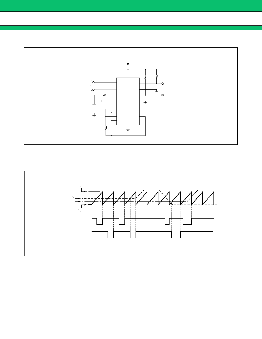
TEST CIRCUIT
s
s
s
s
OPERATING TIMING
V
CC
V
CC
=
15V
OUTPUT
1
OUTPUT
2
C
1
E
1
C
2
E
2
V
REF
GND
V
D
V
C
DT
FB
R
T
C
T
30 k
1000 pF
TEST
INPUT
50 k
-
IN1
-
IN2
+
IN1
+
IN2
OC
150
/2 W
150
/2 W
3.0 V
0 V
V
C
V
D
OUTPUT 1
OUTPUT 2
ON
ON
ON
ON
ON
ON
ON
=
=
Voltage at
C
T

MB3759
7
s
s
s
s
OSCILLATION FREQUENCY
s
s
s
s
OUTPUT LOGIC TABLE
Input (Output Control)
Output State
GND
Single-ended or parallel output
V
REF
Push-pull
f
OSC
R
T
∑
C
T
1.2
C
T
: µF
R
T
: k
fosc : kH
Z
=
MB3759
8
s
s
s
s
TYPICAL CHARACTERISTICS
(Continued)
5
6
3
4
1
2
0
V
REF
V
REF
I
O
= 1 mA
0
10
20
30
40
5
0
-
5
10
0
-
10
-
20
-
25
-
30
50
0
25
75
100
V
CC
= 15 V
I
O
= 1 mA
Reference voltage V
REF
(V)
Temperature Ta (∞C)
Oscillator vs. R
T
, C
T
Duty ratio vs. dead time control voltage
Oscillator frequency f
OS
C
(H
Z
)
Reference voltage change
V
REF
(mV)
Power supply voltage V
CC
(V)
Reference voltage vs.
power supply voltage
Reference voltages. temperature
V
CC
=15 V
C
T
= 470 pF
1000 pF
0.01
µ
F
0.1
µ
F
V
CC
= 15 V
C
T
=
1000 pF
R
T
= 30 k
Ta = 0
∞
C
Ta = +70
∞
C
1 M
500 k
200 k
100 k
50 k
20 k
10 k
5 k
2 k
1 k
2 k
5 k 10 k 20 k
100 k 200 k 500 k
R
T
(
)
0
10
20
30
40
50
1
2
3
0
Ta = +25
∞
C
Duty radio T
ON
/ T (%)
Dead time control voltage V
D
(V)
Reference voltage change
V
REF
(mV)
MB3759
9
(Continued)
V
CC
= 15 V
V
O
= 3 V
I
OL
I
OH
0
0
0.5
5
1.0
10
1.5
15
1
2
3
4
5
0
0.2
0.4
0.6
0.8
V
CC
= 15 V
Ta = 0
∞
C
V
OL
Ta = +25
∞
C
V
OH
Ta = +70∞C
Ta = +70
∞
C
Ta = +25
∞
C
100
90
80
70
60
20
10
0
50
40
30
10
100
1 k
10 k
100 k
1 M
Ta = 0
∞
C
Open loop voltage amplification vs. frequency
Frequency f (H
z
)
Output voltage vs. output current
(feed back terminal)
Low - level output voltage V
OL
(V
)
High - level output voltage V
OH
(V)
Output current I
OL
, I
OH
(mA)
Open loop voltage amplification A
V
(dB)
0.4
0.6
0.8
1.0
1.2
V
CC
= 15 V
Ta = 0
∞
C
Ta = +25
∞
C
1.0
1.2
1.4
1.6
1.8
0
50
100
150
200
0
50
100
150
200
V
CC
= 15 V
Ta = +70
∞
C
Ta = 0
∞
C
Ta = +25
∞
C
Ta = +70
∞
C
Collector saturation voltage vs.
collector output current
Collector output current I
C
(mA)
Emitter saturation voltage vs.
emitter output current
Emitter saturation v
o
ltage V
SAT
(E
)
(V)
Emitter output current I
E
(mA)
Collector saturation voltage V
SAT
(
C
)
(V)
MB3759
10
(Continued)
V
OUT
400
0
2.5
5
7.5
10
0
1
2
3
6
0
10
20
30
40
I
CC
I
CCQ
5 V
4
5
6
4
5
3
1
2
0
8
Output voltage vs. reference voltage
Output voltage V
OUT
(V)
Reference voltage V
REF
(V)
Power supply current vs. power supply voltage
Power supply current I
CC
,I
CCQ
(mA)
Power supply voltage V
CC
(V)
0
200
1000
0
20
40
60
80
100
800
400
600
SOP
0
200
1000
800
400
600
0
10
20
30
40
Ta = +25
∞
C
(200, 10)
(100, 10)
(200, 5)
(100, 5)
(100, 0)
(0, 0)
(I
O
, I
R
)
(mA)
Power dissipation vs. power supply voltage
Power dissipation P
D
(mW)
Power supply voltage V
CC
(V)
Power dissipation vs. ambient temperature
Power dissipation P
D
(mW)
Temperature T
a
(
∞
C)
plastic DIP
ceramic DIP
MB3759
11
s
s
s
s
BASIC OPERATION
Switching regulators can achieve a high level of efficiency. This section describes the basic principles of operation
using a chopper regulator as an example.
As shown in the diagram, diode D provides a current path for the current through inductance L when Q is off.
Transistor Q performs switching and is operated at a frequency that provides a stable output. As the switching
element is saturated when Q is on and cutoff when Q is off, the losses in the switching element are much less
than for a series regulator in which the pass transistor is always in the active state.
While Q is conducting, the input voltage V
IN
is supplied to the LC circuit and when Q is off, the energy stored in
L is supplied to the load via diode D. The LC circuit smooths the input to supply the output voltage.
The output voltage V
O
is given by the following equation.
As indicated by the equation, variation in the input voltage is compensated for by controlling the duty cycle (Ton/
T). If V
IN
drops, the control circuit operates to increase the duty cycle so as to keep the output voltage constant.
The current through L flows from the input to the output when Q is on and through D when Q is off. Accordingly,
the average input current I
IN
is the product of the output current and the duty cycle for Q.
The theoretical conversion efficiency if the switching loss in Q and loss in D are ignored is as follows.
The theoretical conversion efficiency is 100%. In practice, losses occur in the switching element and elsewhere,
and design decisions to minimize these losses include making the switching frequency as low as practical and
setting an optimum ratio of input to output voltage.
V
O
=
Ton + Toff
Ton
V
IN
=
T
Ton
V
IN
Q : ON
L
Q : OFF
Q
D
V
IN
C
V
O
R
L
Q: Switching element
D: Flywheel diode
I
IN
=
T
Ton
I
O
=
P
IN
P
O
◊
100 (%)
=
V
IN
∑
I
IN
V
O
∑
I
O
◊
100
=
V
IN
∑
I
O
∑
Ton / T
V
IN
∑
I
O
∑
Ton / T
◊
100
=
100 (%)
MB3759
12
s
s
s
s
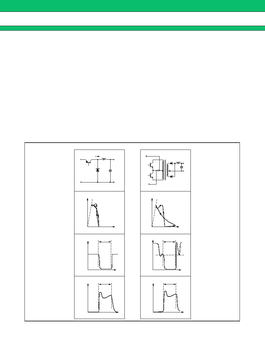
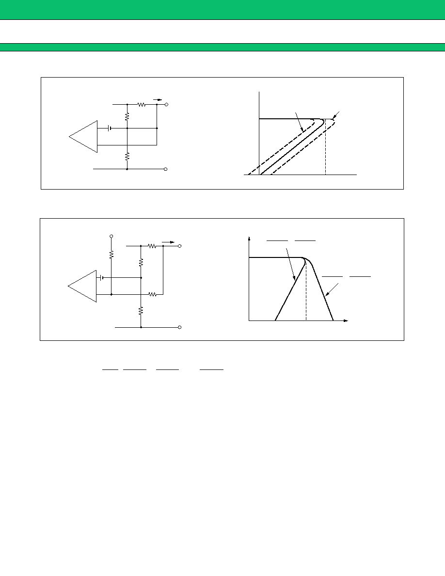
SWITCHING ELEMENT
1.
Selection of the Switching Transistor
It can be said that the success or otherwise of a switching regulator is determined by the choice of switching
transistor. Typically, the following parameters are considered in selecting a transistor.
∑ Withstand voltage
∑ Current
∑ Power
∑ Speed
For the withstand voltage, current, and power, it is necessary to determine that the area of safe operation (ASO)
of the intended transistor covers the intended range for these parameters.
The speed (switching speed: rise time tr, storage time tstg, and fall time tf) is related to the efficiency and also
influences the power.
The figures show the transistor load curve and V
CE
- I
C
waveforms for chopper and inverter-type regulators.
The chopper regulator is a relatively easy circuit to deal with as the diode clamps the collector. A peak can be
seen immediately after turn-on. However, this is due to the diode and is explained later.
In an inverter regulator, the diodes on the secondary side act as a clamp. Viewed from the primary side, however,
a leakage inductance is present. This results in an inductive spike which must be taken account of as it is added
to double the V
IN
voltage.
IN
Q
D
C
V
O
L
I
C
V
CE
on
IN
D1
D2
L
V
O
I
C
on
off
V
IN
2 V
IN
V
CE
Ton
V
CE
2 V
IN
V
IN
t
Ton
I
C
t
Ton
I
C
V
CE
Ton
I
C
off
V
IN
V
CE
t
C
t
chopper regulator
inverter regulator
MB3759
13
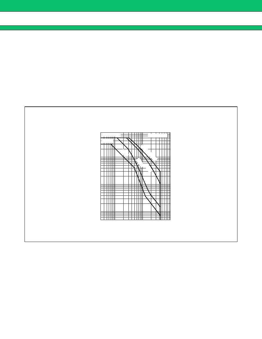
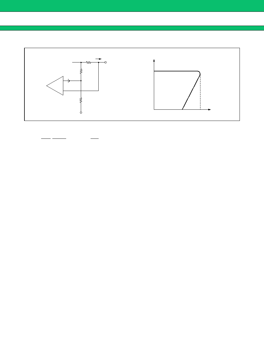
The figure below shows an example of the ASO characteristics for a forward-biased power transistor (2SC3058A)
suitable for switching.
Check that the ASO characteristics for the transistor you intend to use fully covers the load curve. Next, check
whether the following conditions are satisfied. If so, the transistor can be expected to perform the switching
operation safely.
∑ The intended ON time does not exceed the ON-time specified for the ASO characteristic.
∑ The OFF-time ASO characteristic satisfies the intended operation conditions.
∑ Derating for the junction temperature has been taken into account.
For a switching transistor, the junction temperature is closely related to the switching speed. This is because the
switching speed becomes slower as the temperature increases and this affects the switching losses.
2.
Selecting the Diode
Consideration must be given to the switching speed when selecting the diode. For chopper regulators in particular,
the diode affects the efficiency and noise characteristics and has a big influence on the performance of the
switching regulator.
If the reverse recovery time of the diode is slower than the turn-on time of the transistor, an in-rush current of
more than twice the load current occurs resulting in noise (spikes) and reduced efficiency.
As a rule for diode selection, use a diode with a reverse recovery time t
rr
that is sufficiently faster than the transistor
t
r
.
2SC3058A (450 V, 30 A)
T
C
= +25∞C
I
C
(Pulse)
max.
I
C
max.
D.C.
Pw = 500
µs
1 ms
10 ms
5
10
20
50
100 200
500 1000
20
50
10
5
2
1
0.5
0.2
0.1
0.05
Forward-biased area of safe operation single pulse
Single pulse
Collector current I
C
(A)
Collector - emitter voltage V
CE
(V)
MB3759
14
s
s
s
s
APPLICATION IN PRACTICAL CIRCUITS
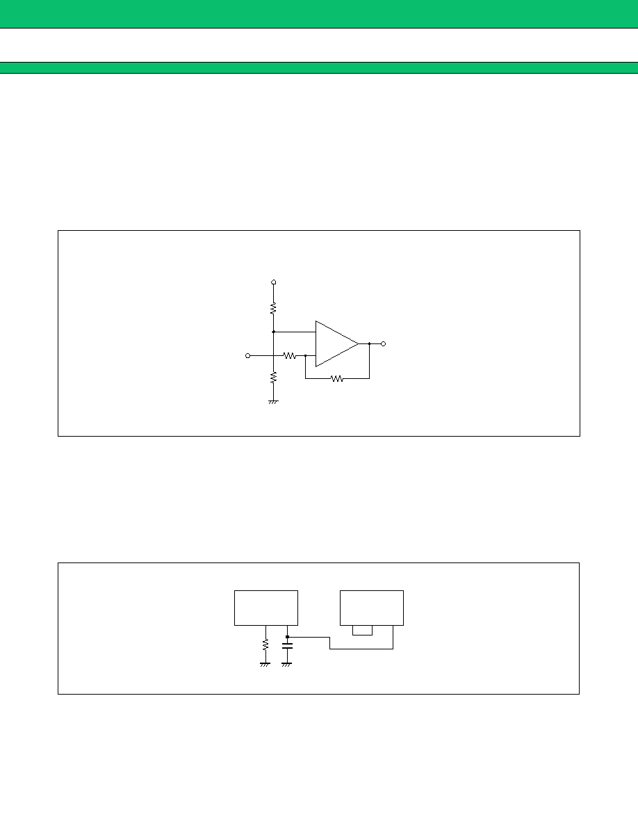
1. Error Amplifier Gain Adjustment
Take care that the bias current does not become large when connecting an external circuit to the FB pin (pin 3)
for adjusting the amplifier gain. As the FB pin is biased to the low level by a sink current, the duty cycle of the
output signal will be affected if the current from the external circuit is greater than the amplifier can sink.
The figure below shows a suitable circuit for adjusting the gain.
It is very important that you avoid having a capacitive load connected to the output stage as this will affect the
response time.
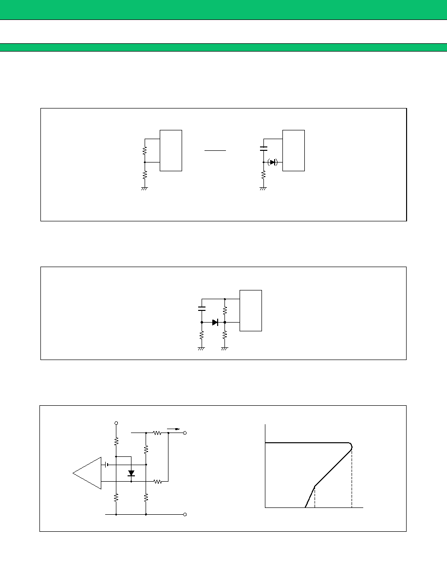
2. Synchronized Oscillator Operation
The oscillator can be halted by connecting the C
T
pin to the GND pin. If supplying the signal externally, halt the
internal oscillator and input to the C
T
pin.
Using this method, multiple ICs can be used together in synchronized operation. For synchronized operation,
set one IC as the master and connect the other ICs as shown in the diagram.
OUT
R
F
V
o
R
IN
R2
R1
V
REF
+
-
R
T
C
T
V
REF
R
T
C
T
Master
Slave
MB3759
15
3. Soft Start
A soft start function can be incorporated by using the dead-time control element.
When the power is turned on, Cd is not yet charged and the DT input is pulled to the V
REF
pin causing the output
transistor to turn off. Next, the input voltage to the DT pin drops in accordance with the Cd, Rd constant causing
the output pulse width to increase steadily, providing stable control circuit operation.
If you wish to use both dead-time and softstart, combine these in an OR configuration.
4. Output Current Limiting (Fallback system using a detection resistor inserted on the output side)
(1) Typical example
V
REF
V
REF
DT
DT
Cd
Rd
R1
R2
V
D
=
R2
R1+R2
V
R
Setting the dead-time
Incorporating soft start
Cd
Rd
R2
R1
DT
V
REF
V
REF
R3
R
S
V
O
R1
R5
R2
R4
V
IO
I
O
GND
V
O
V
O1
0
0
I
L3
I
L2
I
O
I
L1
+
-
D

MB3759
16
∑ Initial limit current I
L1
As the diode is reverse biased
V
IO
is the input offset voltage to the op-amp (-10 mV
V
IO
+10 mV) and this causes the variation in I
L
. Accordingly,
if for example the variation in I
L
is to be limited to
±
10 %, using equation (1) and only considering the variation
in the offset voltage gives the following:
This indicates a setting of 100 mV or more is required.
∑ Polarity change point I
L2
As this is the point where the diode becomes forward biased, it can be calculated by substituting [R4/(R3+R4)
V
REF
- V
D
] for V
O
in equation (where V
D
is the forward voltage of the diode).
∑ Final limit current I
L3
The limit current for V
O
= 0 when R2 >> R1 is the point where the voltages on either side of R
S
and on either
side of R5 are biased.
R3//R4 is the resistance formed by R3 and R4 in parallel (R3R4/(R3 + R4)). When R3//R4 << R5, equation (2)
becomes:
In addition to determining the limit current I
L3
for V
O
= 0, R3, R4, R5, and diode D also operate as a starter when
the power is turned on.
∑ Starter circuit
The figure below shows the case when the starter circuit formed by R3, R4, R5, and D is not present. The output
current I
O
after the operation of the current limiting circuit is:
When V
O
= 0 such as when the power is turned on, the output current I
O
= -V
I O
/ R
S
and, if the offset voltage V
IO
is positive, the output current is limited to being negative and therefore the output voltage does not rise.
Accordingly, if using a fallback system with a detection resistor inserted in the output, always include a starter
circuit, expect in the cases described later.
V
O
>
R3
+
R4
R4
V
REF
The condition for V
O
is:
R
S
I
L1
=
R1 + R2
R1
V
O
≠ V
IO
I
L1
=
R1 + R2
R1
R
S
V
O
R
S
V
IO
≠
Eq. (1) (where R2 >> R1)
R1
+
R2
R1
( V
O
+
V
EE
)
-
( R2
>>
R1
)
I
O
=
R
S
1
R
S
V
IO
R
S
V
IO
I
L2
=
R1
+
R2
R1
R
S
R4
/
(R3
+
R4)
∑
V
REF
≠
V
D
≠
R
S
I
L3
=
R3R4
+
R3R5
+
R4R5
R4R5 V
REF
-
R3R5
V
D
-
R4R5
V
D
-
V
IO
(2)
R
S
V
IO
I
L3
=
R
S
1
(
R3
+
R4
R4
V
REF
-
V
D
)
-
1
+
(R
3
//
R
4
)
/
R
5
1
Eq.
R
S
V
IO
I
L3 C
=
R
S
1
(
R3
+
R4
R4
V
REF
≠
V
D
) ≠
I
O
=
R1
+
R2
R1
R
S
V
O
R
S
V
IO
-
MB3759
17
(2) Example that does not use a diode
The output current I
O
after current limiting is:
In this case, a current flows into the reference voltage source via R3 and R4 if V
O
> V
REF
. To maintain the stability
of the reference voltage, design the circuit such that this does not exceed 200 µA.
R
S
V
O
R1
R2
V
IO
I
O
GND
V
O
V
O
0
I
O
I
L1
V
IO
> 0
V
IO
< 0
+
-
V
O
R1
R1
+
R2
>
I
O
R
S
V
O
R1
R4
R2
GND
0
0
R3
V
IO
V
REF
+
-
V
O
R4
R3
+
R4
R1
R1
+
R2
<
R4
R3
+
R4
I
O
I
L1
I
O
=
R
S
1
[(
R1
+
R2
R1
≠
V
REF
≠ V
IO
] (R2
>>
R1)
R3
+
R4
R4
) V
O
+
R3
+
R4
R4
MB3759
18
(3) When an external stabilized negative power supply is presen
t
The output current I
O
after current limiting is:
If the output is momentarily shorted, V
O
* goes briefly negative. In this case, set the voltage across R1 to
300 mV or less to ensure that a voltage of less than -0.3 V is not applied to the op-amp input.
R1
R2
V
IO
-
V
EE
R
S
V
O
*
V
O
V
O
V
O
0
0
I
L5
I
L1
I
O
I
O
+
-
I
O
=
R
S
1
R1
+
R2
R1
≠
(V
O
+
V
EE
)
R
S
V
IO
(R2
>>
R1)
MB3759
19
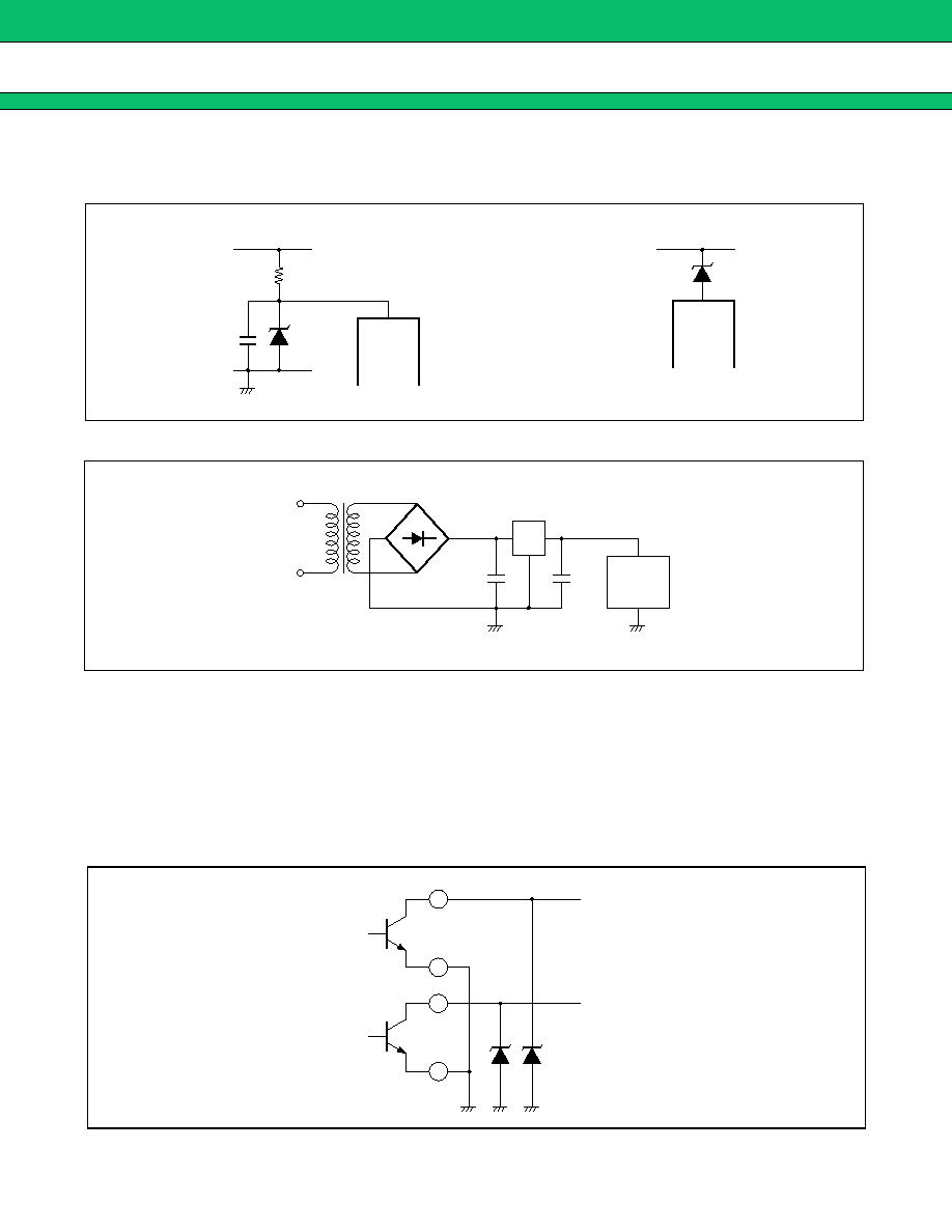
5. Example Power Supply Voltage Supply Circuit
(1) Supplied via a Zener diode
(2) Supplied via a three-terminal regulator
6. Example Protection Circuit for Output Transistor
Due to its monolithic IC characteristics, applying a negative voltage greater than the diode voltage ( := 0.5 V) to
the substrate (pin 7) of the MB3759 causes a parasitic effect in the IC which can result in misoperation.
Accordingly, the following measures are required if driving a transformer or similar directly from the output
transistor of the IC.
(1) Protect the output transistor from the parasitic effect by using a Schottky barrier diode.
V
CC
= V
Z
R
C
MB3759
V
CC
MB3759
V
CC
= V
IN
-
V
Z
V
IN
V
Z
V
IN
V
Z
V
CC
AC
V
CC
MB3759
Three-terminal
regulator
8
9
11
SBD
10
MB3759
20
(2) Provide a bias at the anode-side of the diode to clamp the low level side of the transistor.
(3) Drive the transformer via a buffer transistor.
8
11
14
7.5 k
0.1 µF
1.2 k
=
0.7 V
V
CC
8
9
MB3759
21
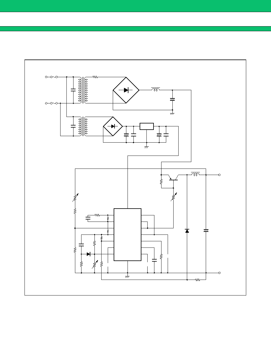
7. Typical Application
(1)Chopper regulator
AC 100 V
1
15 V
50
2 k
1 mH
24 V
2.5 A
2200
µ
F
10 k
100 k
10 k
16 k
5.1 k
0.22
µ
F
10
µ
F
47 k
2.2 k
5.6 k
5 k
300
5.1 k
2200 pF
0.1
FB
-
IN1
V
REF
-
IN2
+
IN1
+
IN2
DT
E
1
C
1
E
2
R
T
C
2
C
T
OC
GND
V
CC
+
20 k
+
+
+
+
MB3759
22
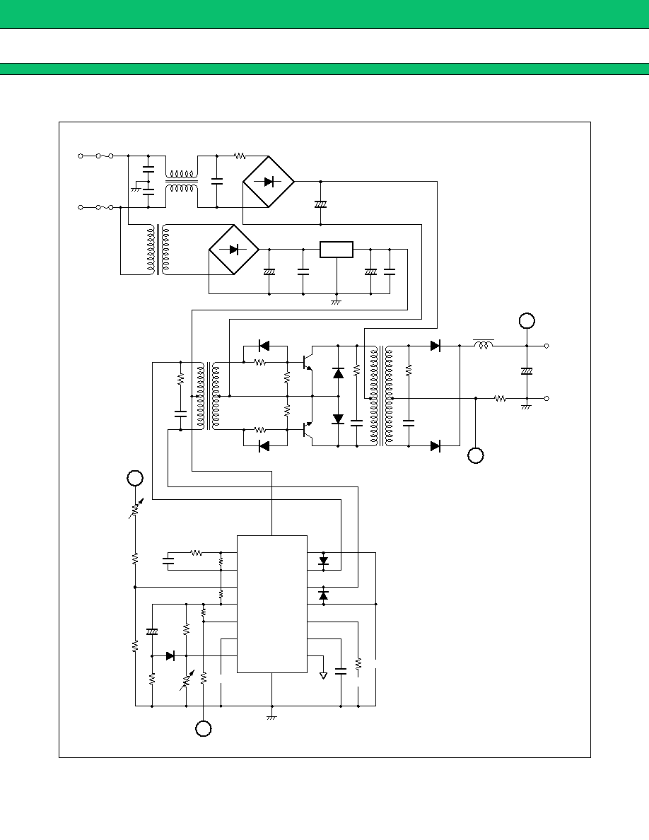
(2) Inverter regulator
AC 100 V
15 V
33
100
100
33
A
B
A
B
300
20 k
10 k
100 k
2.2 k
5.6 k
0.1
5.1 k
16 k
10 k
5.1 k
REF
5 k
10 µF
47 k
V
REF
E
1
C
1
C
2
E
2
R
T
OC
C
T
FB
GND
0.22 µF
2200
µ
F
+
IN1
-
IN2
+
IN2
-
IN1
24 V
2.5 A
DT
V
CC
+
+
+
+
2200 pF
+

MB3759
23
s
s
s
s
ORDERING INFORMATION
Part number
Package
Remarks
MB3759P
16-pin plastic DIP
(DIP-16P-M04)
MB3759C
16-pin ceramic DIP
(DIP-16C-C01)
MB3759PF
16-pin plastic SOP
(FPT-16P-M06)
MB3759
24
s
s
s
s
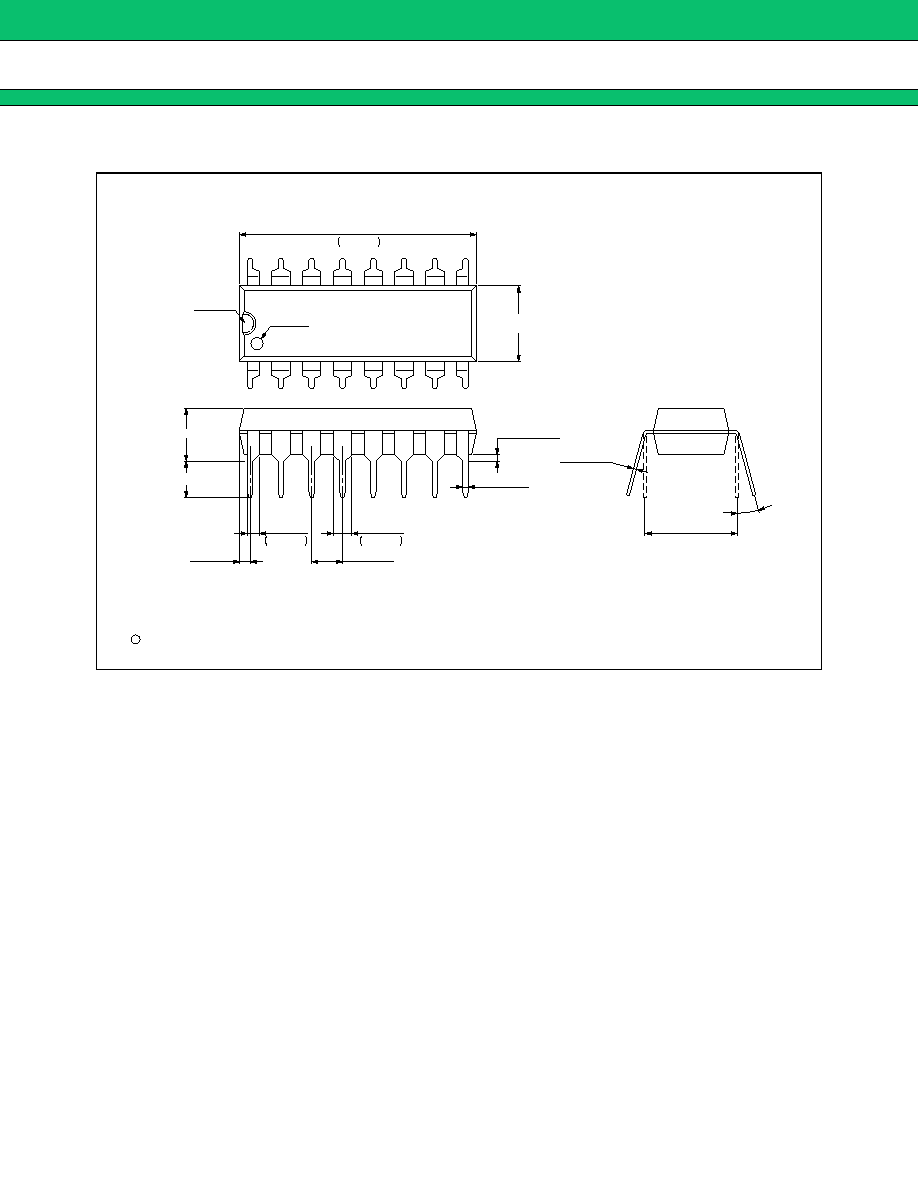
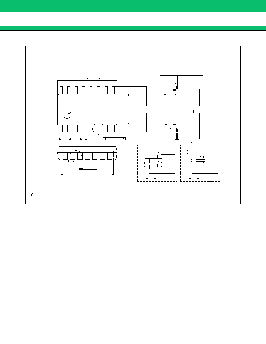
PACKAGE DIMENSIONS
(Continued)
16-pin plastic DIP
(DIP-16P-M04)
Dimensions in mm (inches)
C
1994 FUJITSU LIMITED D16033S-2C-3
0.46±0.08
(.018±.003)
INDEX-2
2.54(.100)
TYP
≠0.30
+0.20
19.55
15∞MAX
0.51(.020)MIN
(.010±.002)
0.25±0.05
1.52
+0.30
≠0
1.27(.050)
MAX
INDEX-1
≠0
+0.30
+.012
≠0
.039
.770
≠.012
+.008
.060
≠0
+.012
7.62(.300)
TYP
6.20±0.25
(.244±.010)
4.36(.172)MAX
3.00(.118)MIN
0.99
MB3759
25
(Continued)
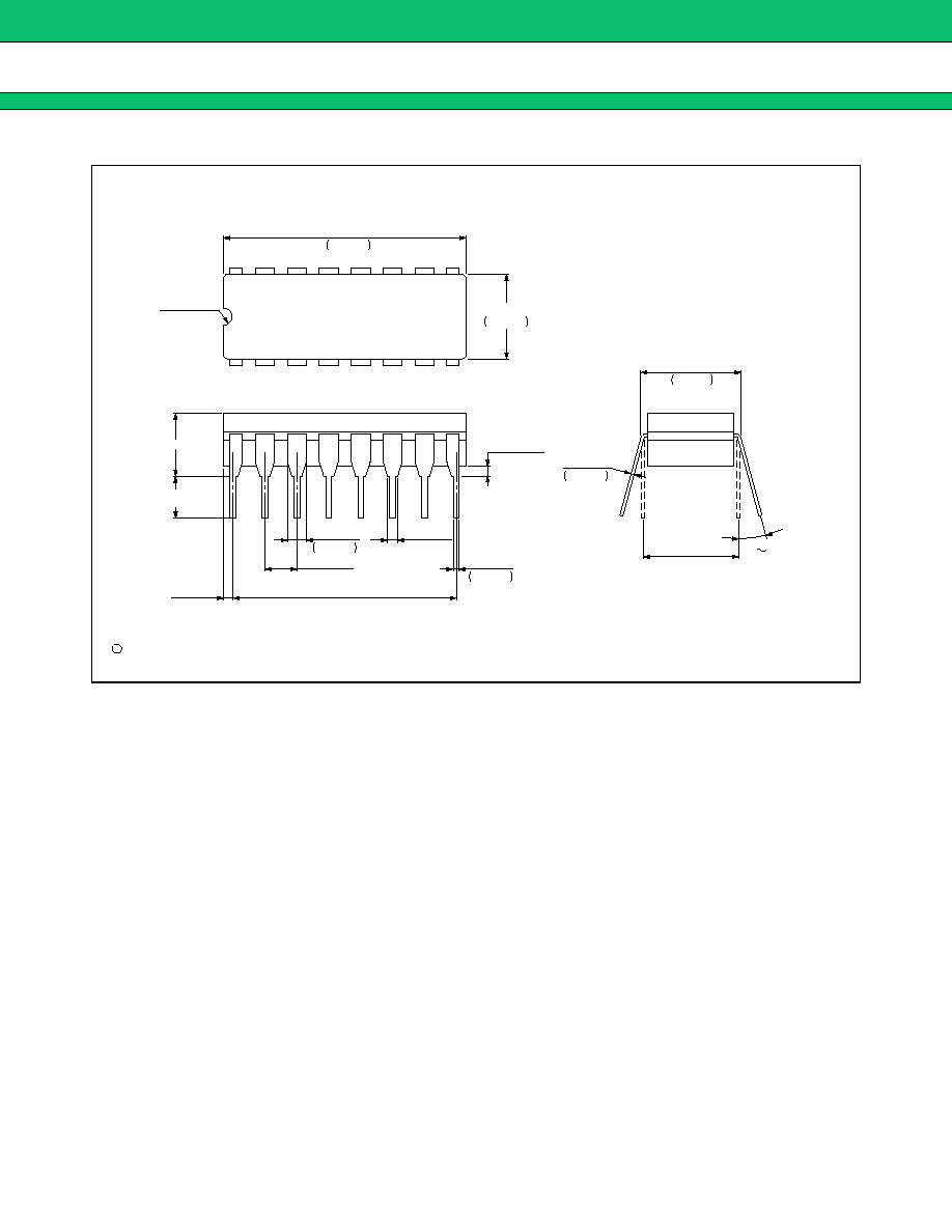
(Continued)
16-pin ceramic DIP
(DIP-16C-C01)
Dimensions in mm (inches)
C
1994 FUJITSU LIMITED D16011SC-2-3
2.54±0.25
(.100±.010)
≠0.15
+0.71
19.30
0∞
1.52
+0.05
≠0.10
1.27(.050)
MAX
R0.64(.025)
≠0.08
+0.13
0.46
15∞
0.25
+0.10
≠0.05
≠0.15
+0.36
7.90
TYP
0.81(.032)
17.78(.700)REF
(.032±.012)
0.81±0.30
6.30
+0.30
≠0.10
REF
+.005
≠.003
.018
.248
≠.004
+.012
+.014
≠.006
.311
.010
≠.002
+.004
7.62(.300)
TYP
+.028
≠.006
.760
.060
≠.004
+.002
5.08(.200)MAX
3.40±0.36
(.134±.014)
MB3759
26
(Continued)
16-pin plastic SOP
(FPT-16P-M06)
Dimensions in mm (inches)
C
2000 FUJITSU LIMITED F16015S-2C-5
ÿ0.13(.005)
M
"A"
0.68(.027)MAX
0.18(.007)MAX
0.40(.016)
0.20(.008)
Details of "A" part
0.45±0.10
0.05(.002)MIN
7.80±0.40
5.30±0.30
0.50±0.20
(.020±.008)
(STAND OFF)
(.018±.004)
(.209±.012)
(.307±.016)
.400
≠.008
+.010
≠0.20
+0.25
10.15
.006
≠.001
+.002
≠0.02
+0.05
0.15
.268
≠.008
+.016
≠0.20
+0.40
6.80
INDEX
TYP
1.27(.050)
8.89(.350)REF
"B"
Details of "B" part
0.20(.008)
0.15(.006)
0.18(.007)MAX
0.68(.027)MAX
2.25(.089)MAX
(Mounting height)
0.10(.004)

MB3759
FUJITSU LIMITED
For further information please contact:
Japan
FUJITSU LIMITED
Corporate Global Business Support Division
Electronic Devices
KAWASAKI PLANT, 4-1-1, Kamikodanaka,
Nakahara-ku, Kawasaki-shi,
Kanagawa 211-8588, Japan
Tel: +81-44-754-3763
Fax: +81-44-754-3329
http://www.fujitsu.co.jp/
North and South America
FUJITSU MICROELECTRONICS, INC.
3545 North First Street,
San Jose, CA 95134-1804, U.S.A.
Tel: +1-408-922-9000
Fax: +1-408-922-9179
Customer Response Center
Mon. - Fri.: 7 am - 5 pm (PST)
Tel: +1-800-866-8608
Fax: +1-408-922-9179
http://www.fujitsumicro.com/
Europe
FUJITSU MICROELECTRONICS EUROPE GmbH
Am Siebenstein 6-10,
D-63303 Dreieich-Buchschlag,
Germany
Tel: +49-6103-690-0
Fax: +49-6103-690-122
http://www.fujitsu-fme.com/
Asia Pacific
FUJITSU MICROELECTRONICS ASIA PTE. LTD.
#05-08, 151 Lorong Chuan,
New Tech Park,
Singapore 556741
Tel: +65-281-0770
Fax: +65-281-0220
http://www.fmap.com.sg/
Korea
FUJITSU MICROELECTRONICS KOREA LTD.
1702 KOSMO TOWER, 1002 Daechi-Dong,
Kangnam-Gu,Seoul 135-280
Korea
Tel: +82-2-3484-7100
Fax: +82-2-3484-7111
F0006
©
FUJITSU LIMITED Printed in Japan
All Rights Reserved.
The contents of this document are subject to change without notice.
Customers are advised to consult with FUJITSU sales
representatives before ordering.
The information and circuit diagrams in this document are
presented as examples of semiconductor device applications, and
are not intended to be incorporated in devices for actual use. Also,
FUJITSU is unable to assume responsibility for infringement of
any patent rights or other rights of third parties arising from the use
of this information or circuit diagrams.
The contents of this document may not be reproduced or copied
without the permission of FUJITSU LIMITED.
FUJITSU semiconductor devices are intended for use in standard
applications (computers, office automation and other office
equipments, industrial, communications, and measurement
equipments, personal or household devices, etc.).
CAUTION:
Customers considering the use of our products in special
applications where failure or abnormal operation may directly
affect human lives or cause physical injury or property damage, or
where extremely high levels of reliability are demanded (such as
aerospace systems, atomic energy controls, sea floor repeaters,
vehicle operating controls, medical devices for life support, etc.)
are requested to consult with FUJITSU sales representatives before
such use. The company will not be responsible for damages arising
from such use without prior approval.
Any semiconductor devices have inherently a certain rate of failure.
You must protect against injury, damage or loss from such failures
by incorporating safety design measures into your facility and
equipment such as redundancy, fire protection, and prevention of
over-current levels and other abnormal operating conditions.
If any products described in this document represent goods or
technologies subject to certain restrictions on export under the
Foreign Exchange and Foreign Trade Control Law of Japan, the
prior authorization by Japanese government should be required for
export of those products from Japan.