 | –≠–ª–µ–∫—Ç—Ä–æ–Ω–Ω—ã–π –∫–æ–º–ø–æ–Ω–µ–Ω—Ç: MB3763PF | –°–∫–∞—á–∞—Ç—å:  PDF PDF  ZIP ZIP |
DS04-29101-5E
FUJITSU SEMICONDUCTOR
DATA SHEET
ASSP
Bidirectional Motor Driver
MB3763
s
s
s
s
DESCRIPTION
Fujitsu's MB3763 Motor Driver with forward/reverse control capability, is used in applications such as the front-
loading mechanism in video tape, or the auto-reverse tape deck, driven by a TTL signal. The MB3763 has 150
mA drive units and braking capability with TTL control.
s
s
s
s
FEATURES
∑ Motor Drive Current: 150 mA maximum (DC)
300 mA maximum (t
ON
=
1 s, Duty
=
50
%
)
∑ Wide Power Supply Voltage Range: 4V to 18V
∑ TTL-control capability
∑ Standby capability when input is off.
∑ Brake capability at motor stop mode.
∑ Built-in diode for surge absorption
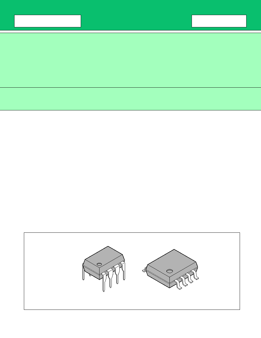
∑ Package:
8-pin plastic DIP package (Suffix: ≠P)
8-pin plastic SOP package (Suffix: ≠PF)
s
s
s
s
PACKAGE
8-pin plastic DIP
8-pin plastic SOP
(DIP-8P-M01)
(FPT-8P-M01)
MB3763
2
s
s
s
s
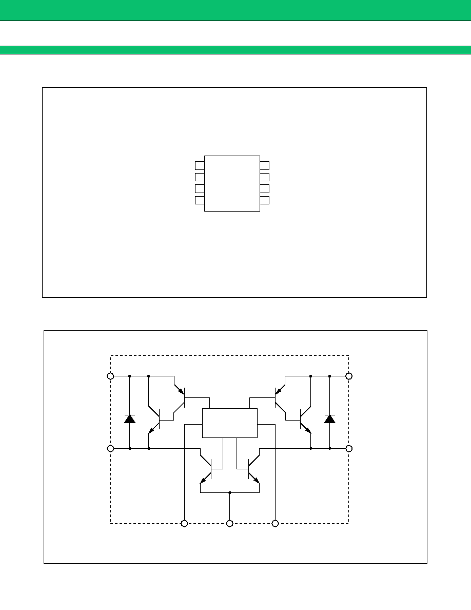
PIN ASSIGNMENT
s
s
s
s
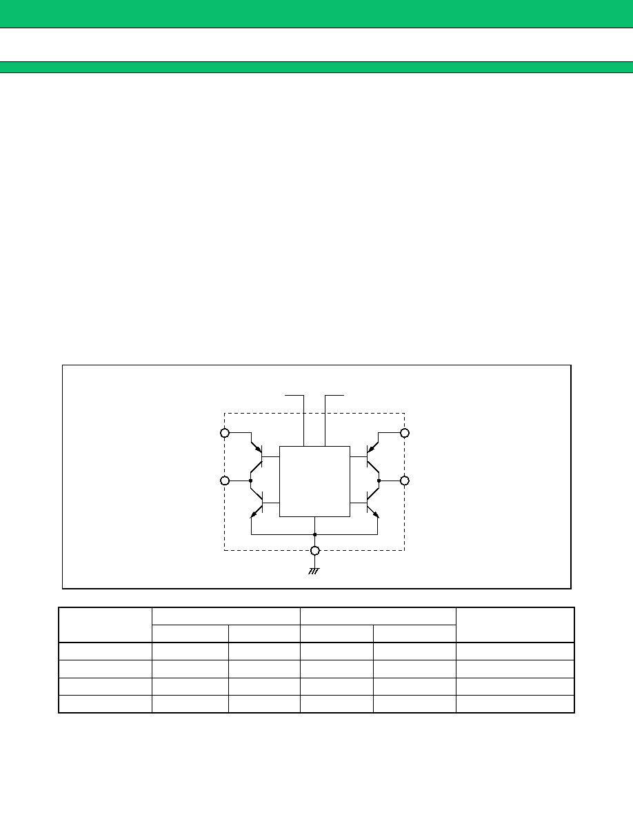
BLOCK DIAGRAM
8
7
6
5
1
2
3
4
A-OUT
A-V
CC
B-V
CC
B-OUT
A-IN
GND
GND
B-IN
(TOP VIEW)
(DIP-8P-M01)
(FPT-8P-M01)
A-V
CC
A-OUT
B-V
CC
B-OUT
A-IN
B-IN
GND
Input
Logic
MB3763
3
s
s
s
s
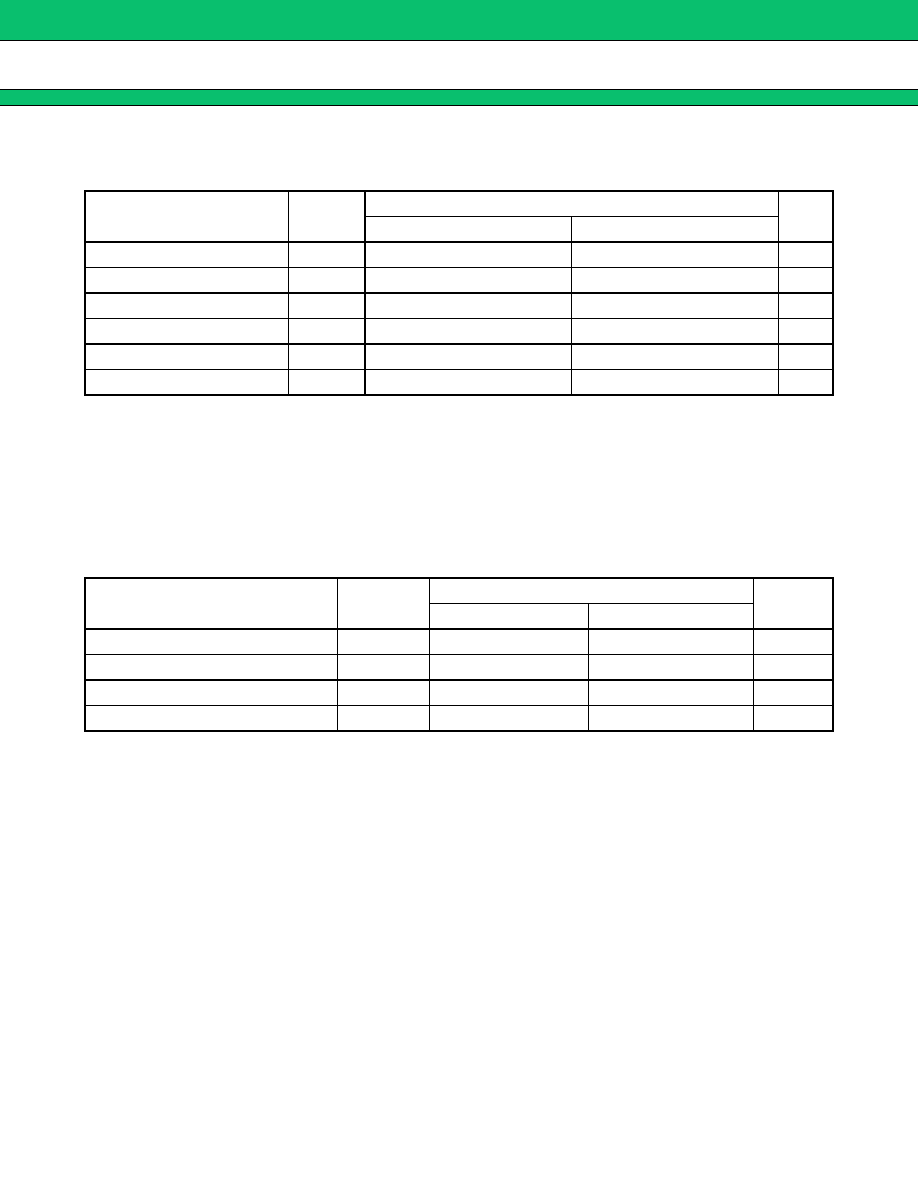
ABSOLUTE MAXIMUM RATINGS
(Ta = +25
∞
C)
*1: t
ON
1 s, Duty = 50%
*2: Ta
60
∞
C
*3: t
5 ms
WARNING: Semiconductor devices can be permanently damaged by application of stress (voltage, current,
temperature, etc.) in excess of absolute maximum ratings. Do not exceed these ratings.
s
s
s
s
RECOMMENDED OPERATING CONDITIONS
*1: t
ON
1 s, Duty = 50%
*2: When V
IH
V
CC
, I
IH
V
CC
◊
0.2 mA
WARNING: The recommended operating conditions are required in order to ensure the normal operation of the
semiconductor device. All of the device's electrical characteristics are warranted when the device is
operated within these ranges.
Always use semiconductor devices within their recommended operating condition ranges. Operation
outside these ranges may adversely affect reliability and could result in device failure.
No warranty is made with respect to uses, operating conditions, or combinations not represented on
the data sheet. Users considering application outside the listed conditions are advised to contact their
FUJITSU representatives beforehand.
Parameter
Symbol
Rating
Unit
Min.
Max.
Power supply voltage
V
CC
20
V
Output current
I
O
180 (330*
1
)
mA
Maximum output current
I
OMAX
*
3
1.2
A
Power Dissipation
P
D
560*
2
mW
Operating temperature
T
C
≠20
+75
∞
C
Storage temperature
Tstg
≠55
+125
∞
C
Parameter
Symbol
Value
Unit
Min.
Max.
Power supply voltage
V
CC
4
18
V
Output current
I
O
0
150 (300*
1
)
mA
Input high voltage
V
IH
*
2
2.4
V
CC
+ 0.3
V
Input low voltage
V
IL
0
0.4
V
MB3763
4
s
s
s
s
ELECTRICAL CHARACTERISTICS
(V
CC
= 12 V, Ta = +25
∞
C)
Parameter
Symbol
Condition
Value
Unit
Min.
Typ.
Max.
Standby supply current
I
CC0
V
CC
= 18 V, V
IA
= V
IB
= 0 V
--
--
1.0
mA
Power supply current
I
CC1
I
O
= 0 mA
--
10
20
mA
I
CC2
I
O
= 150 mA
--
10
--
mA
I
O
= 300 mA
--
15
--
mA
I
CC3
I
O
= 0 mA, V
IA
= V
IB
= 2.4 V
--
15
--
mA
Output high voltage
V
OH
I
O
= 150 mA
11.0
11.2
--
V
I
O
= 300 mA
10.8
11.1
--
V
Output low voltage
V
OL
I
O
= 150 mA
--
0.1
0.2
V
I
O
= 300 mA
--
0.2
0.5
V
Output saturation voltage
V
SAT
I
O
= 150 mA
--
0.9
1.2
V
I
O
= 300 mA
--
1.1
1.7
V
Input current
I
IH
V
IN
= 2.4 V
--
250
400
µ
A
Input switching
prohibition time
T
OFF
--
10
--
--
µ
s
MB3763
5
s
s
s
s
FUNCTIONAL DESCRIPTIONS
FORWARD/REVERSE MODE (MODE B& C)
In this mode, the transistor pairs Q2-Q3 and Q1-Q4 work alternatively, changing the output current direction.
When the mode B is selected, Q2 and Q3 are active and Q1 and Q4 are inactive. Therefore A-OUT is at low
level and B-OUT is at high level, with the current flowing from B-OUT to A-OUT through the motor. On the other
hand, when the mode C is selected, the current flows in the reverse direction.
BRAKE/STOP MODE (MODE A)
When the mode A is selected, Q1 and Q3 are inactive and Q2 and Q4 are active. A-OUT and B-OUT are stuck
at low-level; terminals of motor are shorted and the motor is forced to stop.
STANDBY MODE (MODE D)
In this mode, all transistors are inactive and the current through the motor does not flow. When the power supply
voltage is applied to A-V
CC
and B-V
CC
, the supply current is still less than or equal to 1 mA.
s
s
s
s
CONTROL MODE
Notes: 1:
2.4V
0:
0.4V
Mode
Input mode
Output mode
Operation
A-IN
B-IN
A-OUT
B-OUT
A
1
1
L
L
short (Brake)
B
1
0
L
H
Forward
C
0
1
H
L
Reverse
D
0
0
--
--
Open (Standby)
A-V
CC
A-OUT
B-IN
A-IN
B-V
CC
B-OUT
Q1
Q2
Q3
Q4
GND
Control
Logic
Control Block Diagram