DS04-27400-7E
FUJITSU SEMICONDUCTOR
DATA SHEET
ASSP For power supply applications
BIPOLAR
Power Supply Monitor
MB3771
s
s
s
s
DESCRIPTION
The Fujitsu MB3771 is designed to monitor the voltage level of one or two power supplies (+5 V and an arbitrary
voltage) in a microprocessor circuit, memory board in large-size computer, for example.
If the circuit's power supply deviates more than a specified amount, then the MB3771 generates a reset signal to
the microprocessor. Thus, the computer data is protected from accidental erasure.
Using the MB3771 requires few external components. To monitor only a +5 V supply, the MB3771 requires the
connection of one external capacitor. The level of an arbitrary detection voltage is determined by two external
resistors. The MB3771 is available in an 8-pin Dual In-Line, Single In-Line Package or space saving Flat Package.
s
s
s
s
FEATURES
∑ Precision voltage detection
(
V
SA
=
4.2 V
±
2.5
%
)
∑ User selectable threshold level with hysterisis (V
SB
= 1.23 V
±
1.5
%
)
∑ Monitors the voltage of one or two power supplies (5 V and an arbitrary voltage,
>
1.23 V)
∑ Usable as over voltage detector
∑ Low voltage output for reset signal (V
CC
= 0.8 V typ.)
∑ Minimal number of external components (one capacitor min.)
∑ Low power dissipation (I
CC
= 0.35 mA typ., V
CC
= 5 V)
∑ Detection threshold voltage has hysteresis function
∑ Reference voltage is connectable.
s
s
s
s
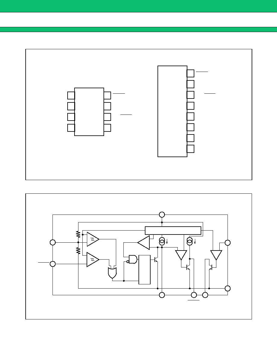
PACKAGES
8-pin plastic DIP
8-pin plastic SIP
8-pin plastic SOIP
(DIP-8P-M01)
(SIP-8P-M03)
(FPT-8P-M01)
MB3771
3
s
s
s
s
FUNCTIONAL DESCRIPTIONS
Comparators Comp.A and Comp.B apply a hysteresis to the detected voltage, so that when the voltage at either
the V
SA
or V
SB
pin falls below 1.23 V the RESET output signal goes to "low" level.
Comp. B may be used to detect any given voltage(Sample Application 3), and can also be used as a forced
reset pin (with reset hold time) with TTL input (Sample Application 6).
Note that if Comp.B is not used, the V
SB
pin should be connected to the V
CC
pin (Sample Application 1).
Instantaneous breaks or drops in the power supply can be detected as abnormal conditions by the MB3771
within a 2
µ
s interval. However because momentary breaks or drops of this duration do not cause problems in
actual systems in some cases, a delayed trigger function can be created by connecting capacitors to the V
SA
or
V
SB
pin (Sample Application 8).
Because the RESET output has built-in pull-up resistance, there is no need to connect to external pull-up
resistance when connected to a high impedance load such as a CMOS logic IC.
Comparator Comp. C is an open-collector output comparator without hysteresis, in which the polarity of input/
output characteristics is reversed. Thus Comp. C is useful for over-voltage detection (Sample Application 11)
and positive logic RESET signal output (Sample Application 7), as well as for creating a reference voltage
(Sample Application 10).
Note that if Comp. C is not used, the V
SC
pin should be connected to the GND pin (Sample Application 1).
s
s
s
s
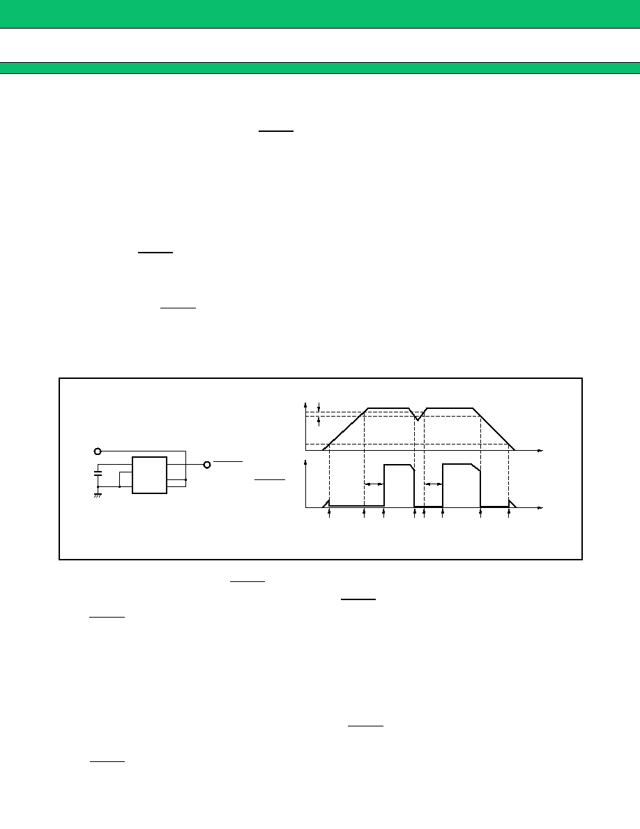
FUNCTION EXPLANATION
(
1
)
When V
CC
rises to about 0.8V, RESET goes low.
(
2
)
When V
CC
reaches V
S
+
V
HYS
, C
T
then begins charging. RESET remains low during this time
(
3
)
RESET goes high when CT begins charging.
T
PO
:= C
T
◊
10
5
(Refer to C
T
pin capacitance vs. hold time )
(4) When V
CC
level dropps lower then V
S
, then RESET goes low and C
T
starts discharging.
(5) When V
CC
level reaches V
S
+ V
HYS
, then C
T
starts charging.
In the case of voltage sagging, if the period from the time V
CC
goes lower than or equal to V
S
to the time V
CC
reaches V
S
+V
HYS
again, is longer than t
PI
, (as specified in the AC Characteristics), C
T
is discharged and charged
successively.
(6) After T
PO
passes, and V
CC
level exceeds V
S
+ V
HYS
, then RESET goes high.
(7) Same as Point 4.
(8) RESET remains low until V
CC
drops below 0.8V.
V
CC
C
T
RESET
1
2
3
4
8
7
6
5
RESET
V
CC
V
S
0.8 V
V
HYS
(1)
(2)
(3)
(4) (5) (6)
(7)
(8)
T
PO
T
PO
t
t
MB3771
4
s
s
s
s
ABSOLUTE MAXIMUM RATINGS
WARNING: Semiconductor devices can be permanently damaged by application of stress (voltage, current,
temperature, etc.) in excess of absolute maximum ratings. Do not exceed these ratings.
s
s
s
s
RECOMMENDED OPERATING CONDITIONS
WARNING: The recommended operating conditions are required in order to ensure the normal operation of the
semiconductor device. All of the device's electrical characteristics are warranted when the device is
operated within these ranges.
Always use semiconductor devices within their recommended operating condition ranges. Operation
outside these ranges may adversely affect reliability and could result in device failure.
No warranty is made with respect to uses, operating conditions, or combinations not represented on
the data sheet. Users considering application outside the listed conditions are advised to contact their
FUJITSU representatives beforehand.
Parameter
Symbol
Rating
Unit
Min.
Max.
Power supply voltage
V
CC
-
0.3
+
20
V
Input voltage
V
SA
-
0.3
V
CC
+
0.3
( < +
20
)
V
V
SB
-
0.3
+
20
V
V
SC
-
0.3
+
20
V
Power dissipation
P
D
200
(
Ta
85
∞
C
)
mW
Storage temperature
Tstg
-
55
+
125
∞
C
Parameter
Symbol
Value
Unit
Min.
Max.
Power supply voltage
V
CC
3.5
18
V
Output current
I
RESET
0
20
mA
I
OUTC
0
6
mA
Operating ambient temperature
Top
-
40
+
85
∞
C
MB3771
5
s
s
s
s
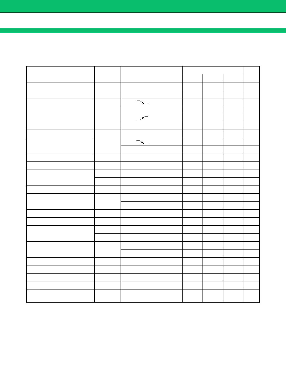
ELECTRICAL CHARACTERISTICS
1.
DC Characteristics
(
V
CC
= 5 V, Ta = + 25
∞
C
)
Parameter
Symbol
Conditions
Value
Unit
Min.
Typ.
Max.
Power supply current
I
CC1
V
SB
= 5 V, V
SC
= 0 V
350
500
µ
A
I
CC2
V
SB
= 0 V, V
SC =
0 V
400
600
µ
A
Detection voltage
V
SAL
(DOWN)
V
CC
4.10
4.20
4.30
V
Ta
=
-
40
∞
C to
+
85
∞
C
4.05
4.20
4.35
V
V
SAH
(UP)
V
CC
4.20
4.30
4.40
V
Ta
=
-
40
∞
C to
+
85
∞
C
4.15
4.30
4.45
V
Hysterisis width
V
HYSA
50
100
150
mV
Detection voltage
V
SB
V
SB
1.212
1.230
1.248
V
Ta
=
-
40
∞
C to
+
85
∞
C
1.200
1.230
1.260
V
Deviation of detection voltage
V
SB
V
CC
= 3.5 V to 18 V
3
10
mV
Hysterisis width
V
HYSB
14
28
42
mV
Input current
I
IHB
V
SB
= 5 V
0
250
nA
I
ILB
V
SB
= 0 V
20
250
nA
"H" level output voltage
V
OHR
I
RESET
=
-
5
µ
A, V
SB
= 5 V
4.5
4.9
V
Output saturation voltage
V
OLR
I
RESET
= 3mA, V
SB
= 0 V
0.28
0.4
V
I
RESET
= 10mA, V
SB
= 0 V
0.38
0.5
V
Output sink current
I
RESET
V
OLR
= 1.0 V, V
SB
= 0 V
20
40
mA
CT charge current
I
CT
V
SB
= 5 V, V
CT
= 0.5 V
9
12
16
µ
A
Input current
I
IHC
V
SC
= 5 V
0
500
nA
I
ILC
V
SC
= 0 V
50
500
nA
Detection voltage
V
SC
1.225
1.245
1.265
V
Ta
=
-
40
∞
C to
+
85
∞
C
1.205
1.245
1.285
V
Deviation of detection voltage
V
SC
V
CC
= 3.5 V to 18 V
3
10
mV
Output leakage current
I
OHC
V
OHC
= 18 V
0
1
µ
A
Output saturation voltage
V
OLC
I
OUTC
= 4 mA, V
SC
= 5 V
0.15
0.4
V
Output sink current
I
OUTC
V
OLC
= 1.0 V, V
SC
= 5 V
6
15
mA
Reset operation minimum
supply voltage
V
CCL
V
OLR
= 0.4 V, I
RESET
= 200
µ
A
0.8
1.2
V