DS04-27211-3E
FUJITSU SEMICONDUCTOR
DATA SHEET
ASSP For Power Supply Applications
BIPOLAR
Switching Regulator Controller
(Supporting External Synchronization)
MB3789
s
DESCRIPTION
The MB3789 is a PWM (pulse width modulation) switching regulator controller supporting an external sync signal.
The MB3789 incorporates two error amplifiers which can be used respectively for voltage control and current
control, allowing the IC to serve as a DC/DC converter with current regulating functions.
The MB3789 is the ideal IC for supplying power to the back-lighting fluorescent tube for a liquid crystal display
(LCD) device such as a camera-integrated VTR.
s
FEATURES
∑ Wide range of operating power supply voltages: 3 V to 18 V
∑ Low current consumption: 1.5 mA (Typ.)
∑ Wide input voltage range of error amplifier: ≠0.2 V to V
CC
≠ 1.8 V
∑ Built-in two error amplifier
∑ Oscillator capable of operating with an external sync signal
∑ Built-in timer latch short protection circuit
∑ Variable dead time provides control over total operating range
∑ Output supporting a power MOSFET
∑ 16-pin SSOP package mountable at high density
s
PACKAGE
16-pin Plastic SSOP
(FPT-16P-M05)

3
MB3789
s
PIN DESCRIPTION
Pin no.
Pin symbol
I/O
Function
7
≠IN1
I
Error amplifier 1 inverting input pin
8
+IN1
I
Error amplifier 1 noninverting input pin
6
FB1
O
Error amplifier 1 output pin
10
≠IN2
I
Error amplifier 2 inverting input pin
9
+IN2
I
Error amplifier 2 noninverting input pin
11
FB2
O
Error amplifier 2 output pin
13
CB
--
Output bootstrap pin.
Connect a capacitor between the CB and OUT pins to bootstrap the
output transistor.
5
SCP
--
Capacitor connection pin for short-circuit protection circuit
12
DTC
I
Dead time control pin
15
OUT
O
Totem-pole output pin
3
C
T
--
Sawtooth waveform frequency setting capacitor/resistor connection
pin
4
SYNC
I
External sync signal input pin
1
V
CC
1
--
Reference power supply, control circuit power-supply pin
14
V
CC
2
--
Output circuit power-supply pin
2
V
REF
O
Reference voltage output pin
16
GND
--
Ground pin
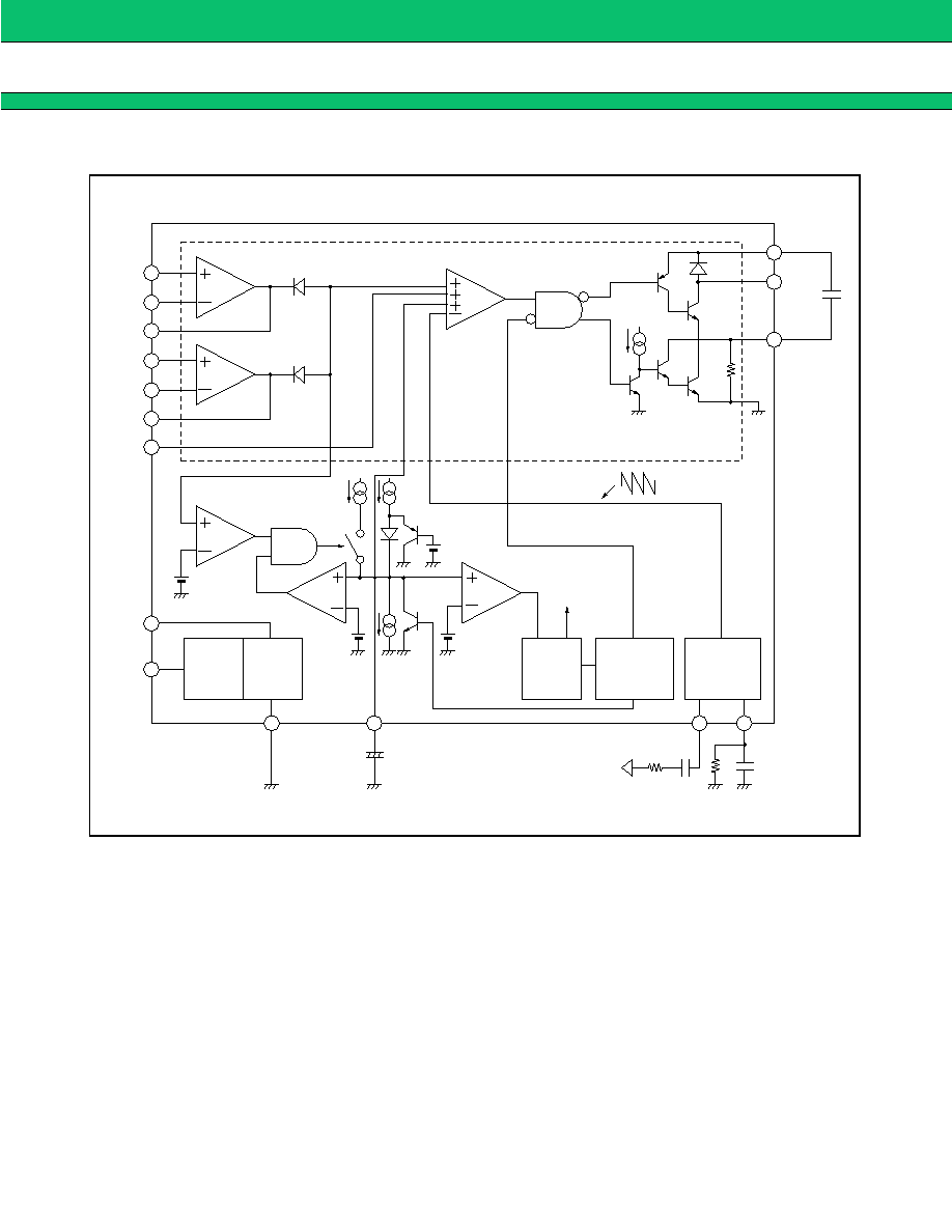
I/O control unit
Sawtooth waveform
oscillator
Power-supply
circuit

5
MB3789
s
FUNCTIONAL DESCRIPTION
1.
Switching Regulator Functions
(1) Reference voltage generator
The reference voltage generator uses the voltage supplied from the power supply pin (pin 1) to generate a
temperature-compensated, reference voltage (about 2.50 V) as the reference supply voltage for the IC's internal
circuitry.
The reference voltage can be output, up to 50
µ
A, to an external device through the V
REF
pin (pin 2).
This regulated reference voltage can be used as the reference voltage for the switching regulator and also
used for setting the dead time.
(2) Sawtooth waveform oscillator
With a timing capacitor and a timing resistor connected to the C
T
pin (pin 3), the sawtooth waveform oscillator
generates a sawtooth wave which remains stable even with supply voltage variations or temperature changes.
The sawtooth wave is input to the PWM comparator. The amplitude of oscillating waveform is 0.3 V to 0.9 V.
In addition, the oscillator can be used for external synchronization, where it generates a sawtooth waveform
synchronous to the input signal from the SYNC pin (pin 4).
(3) Error amplifiers
The error amplifiers detect the output voltage from the switching regulator and outputs the PWM control signal.
Since they support a wide range of in-phase input voltages from ≠0.2 V to "V
CC
≠ 1.8 V", they can be set easily
from an external power supply.
An arbitrary loop gain can be set by connecting a feedback resistor and capacitor from the error amplifier output
pin to the inverting input pin, enabling stable phase compensation to the system.
The MB3789 can make a current-regulated DC/DC converter using the two internal error amplifiers respectively
for voltage control and current control.
(4) PWM comparator
The PWM comparator is a voltage comparator with one inverting input and three noninverting inputs, serving
as a voltage-pulse width converter for controlling the output duty depending on the input voltage.
The PWM comparator turns on the output transistor during the interval in which the sawtooth wave voltage
level is lower than the voltage levels at all of the error amplifier output pins, the SCP pin (pin 5), and at the
DTC pin (pin 12).
(5) Output circuit
The output circuit is a power MOSFET driven, output circuit in a totem-pole configuration. It can drive the gate
voltage up to near the supply voltage with a bootstrap capacitor connected between the OUT pin (pin 15) and
CB pin (pin 13). (See "
s
SETTING THE BOOTSTRAP CAPACITOR (C
BS
).")
2.
Protection Functions
(1) Timer-latch short-circuit protection circuit
SCP comparator 1 detects the output voltage levels of error amplifiers 1 and 2. When the output voltage level
of either (or both) of the two error amplifiers reaches 1.25 V, the timer circuit is actuated to start charging the
external protection-enable capacitor connected to the SCP pin (pin 5).
If the error amplifier output is not restored to the normal voltage level before the capacitor voltage reaches
1.8 V, the latch circuit is actuated to turn off the output transistor while making the dead time 100%.
To reset the actuated protection circuit, turn the power supply on back. (See "
s
SETTING THE SOFT START/
SHORT-CIRCUIT DETECTION TIME.")