DS04-27502-3E
FUJITSU SEMICONDUCTOR
DATA SHEET
ASSP For Power Supply Applications
Bi-CMOS
Battery Backup IC
MB3790
s
DESCRIPTION
The MB3790 is designed to control power supplies to SRAM, logic IC, or other circuit devices and protects them
against momentary power failures by using backup batteries. In addition to its function to supply the power to
these devices, it has a function to switch the source of power to the primary or secondary backup battery when
the power supply voltage drops below a predetermined level. Also, it outputs a reset signal when the power supply
turns on or off or when a fault occurs in the power supply.
Ideally designed as a single-chip IC for power supply control, the MB3790 consumes only a minimal current and
comes in a thin-type package. Therefore, it is best suited for power supply control in memory cards and similar
other devices.
s
FEATURES
∑ Input circuit current consumption when non-loaded: 50
µ
A [typ]
∑ Output drive current: 200 mA [max]
∑ Resistance between input and output: 0.5 ohms [typ]
∑ Input power-down detection level: 4.2 V ± 2.5 %
∑ On-chip power-on reset circuit
∑ Primary battery voltage-down detection levels: 2.65 V, 2.37 V
(Continued)
s
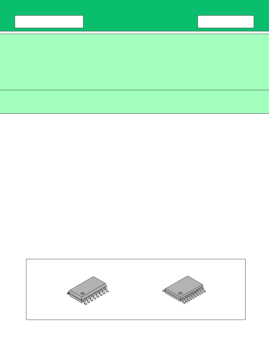
PACKAGES
* : Since the SSOP is an extremely thin package, use a partial heating method when mounting the device.
Plastic SOP, 16 pin
(FPT-16P-M06)
Plastic SSOP*, 20 pin
(FPT-20P-M04)

4
MB3790
s
PIN DESCRIPTION
Pin number
Symbol
I/O
Name and function
16P
20P
1
1
N.C.
--
Non connection
2
2
V
BATI
I
This pin connects to the primary battery.
3, 4
3, 4
V
OUT
O
These pins supply the output voltage. (Range of output current value
I
OUT
200 mA)
5
5
V
BAT2
I/O
This pin connects to the secondary battery. When the power supply
voltage is greater than or equal to the detection level (i.e., V
INH
), the
secondary battery is recharged using the constant-voltage method of
charging.
--
6, 7
N.C.
--
Non connection
6
8
ALARM1
O
This is an open-collector output pin for a primary battery alarm
signal. When the power supply voltage is greater than or equal to
V
INH
, it monitors the primary battery voltage. If the power supply
voltage is less than V
INL
, it does not monitor the primary battery
voltage. If V
BAT1
is less than or equal to 2.65 V, its output voltage is
forced to a Low level.
7
9
ALARM2
O
This is an open-collector output pin for a primary battery alarm
signal. When the power supply voltage is greater than or equal to
V
INH
, it monitors the primary battery voltage. If the power supply
voltage is less than V
INL
, it does not monitor the primary battery
voltage. If V
BAT1
is less than or equal to 2.37 V, its output voltage is
forced to a Low level.
8
10
GND
--
This pin connects to the ground (0 V).
9
11
RESET
O
This pin outputs a reset signal. When the power supply voltage is
less than or equal to V
INL
, it outputs a High level.
If the power supply voltage of SRAM is less than the designated
range, it directly controls the CE or CS of SRAM to disable writes and
thereby protect the data in memory.
10
12
RESET
O
This pin outputs an inverted signal of RESET.
11
13
C
T
--
This pin is used to set the reset pulse width.
Insert a capacitor between this pin and GND to set the pulse width.
--
14, 15
N.C.
--
Non connection
12
16
V
SENSE
I
This pin accepts comparator input for detecting the power supply
voltage level. For details, refer to APPLICATION in this data sheet.
13, 14
17, 18
V
IN
I
These pins accept the input voltage for the device.
15
19
N.C.
--
Non connection
16
20
CONTROL
I
This pin is used for output control. For details, refer to APPLICATION
in this data sheet.

5
MB3790
s
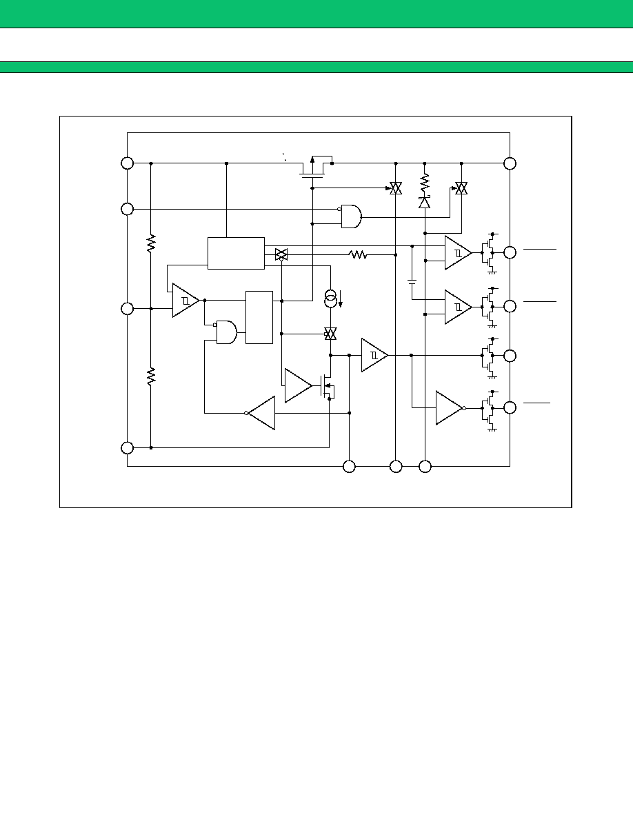
FUNCTIONAL DESCRIPTION
1.
Battery Backup Function
∑ When the power supply voltage exceeds the voltage detection level (i.e., V
INH
), the device outputs a current of
up to 200 mA from the V
IN
power supply to the load circuit via the V
OUT
pin.
∑ When the power supply voltage is less than or equal to V
INL
, the device switches the source of power for V
OUT
from V
IN
to the primary or secondary battery for backup purposes.
2.
Power Supply Voltage Level Detect Function
When the power supply voltage drops below V
INL
, the voltage level detection comparator is actuated to perform the
following (note that the detection voltage level has the hysteresis characteristics listed in ELECTRICAL CHARAC-
TERISTICS in this data sheet):
∑ The comparator first outputs the RESET signal (High level).
∑ It switches the source of power for the load circuit to the primary or secondary battery.
The power supply voltage detection level can be adjusted by fitting an external resistor to the V
SENSE
pin. When
adjusting the detection level, be sure to set it to 4.0 V or higher by considering the power supply voltage for the
internal circuit operation.
In addition, the detection set time can be extended by connecting a capacitator. For this method of adjustment, refer
to APPLICATION in this data sheet.
3.
Reference Voltage Circuit
This is a temperature-compensated reference voltage circuit of a band gap type so that it outputs a trimming-
adjusted exact reference voltage.
The reference voltage power supply is used to set the reference voltage/constant current values of the detection
circuit, as well as the secondary battery recharging voltage.
4.
Power-on Reset Function
By charging the capacitator connected to the C
T
pin with constant current (approx. 3
µ
A), this function determines
the reset pulse width. The calculation formula for this is given below:
Reset pulse width t
PO
(sec)
C
T
(F)
◊
10
6
(When C
T
= 1000 pF, t
PO
1 ms [typ])
5.
Primary Battery Voltage Detection Function
If the primary battery voltage drops below the detection level when the power supply voltage is greater than or equal
to V
INL
, the device outputs an alarm signal (Low level) from the CMOS output pin, ALARM1 or ALARM2.
Note that the voltage level detection comparator has the hysteresis characteristics listed in ELECTRICAL CHAR-
ACTERISTICS in this data sheet.
∑ When the primary battery voltage is 2.65 V [typ] or less:
The ALARM1 output pin is forced to a Low level to issue an alarm indicating that it's time to replace the primary
battery.
∑ When the primary battery voltage is 2.37 V [typ] or less:
The ALARM2 output pin is forced to a low level to issue an alarm indicating that the primary battery voltage
is less than the voltage necessary to retain the SRAM data (approx. 2.0 V)
6.
Secondary Battery Recharging Function
When the power supply voltage is greater than or equal to V
INL
, the device recharges the secondary battery using
the constant-voltage method of charging. Note that the typical value of the device's internal recharging resistor is
500 ohms.