 | –≠–ª–µ–∫—Ç—Ä–æ–Ω–Ω—ã–π –∫–æ–º–ø–æ–Ω–µ–Ω—Ç: MB3800 | –°–∫–∞—á–∞—Ç—å:  PDF PDF  ZIP ZIP |
DS04-27212-2E
FUJITSU SEMICONDUCTOR
DATA SHEET
ASSP For Power Supply Applications
BIPOLAR
Switching Regulator Controller
(Low Voltage)
MB3800
s
DESCRIPTION
The MB3800 is a single-channel switching regulator control IC for low voltage applications incorporating a soft
start function and short circuit detection function. The device has a low minimum operating voltage of 1.8 V and
is ideal for the power supply of battery-operated electronic equipment.
s
FEATURES
∑ Wide supply voltage operating range: 1.8 to 15 V
∑ Low current consumption: Typically 5.5 mA in operation, 1
µ
A or less in stand-by
∑ High speed operation is possible: Maximum 1 MHz
∑ The error amplifier gain is set inside the IC, so peripheral components are minimized.
∑ Incorporates a soft start circuit.
∑ Incorporates a timer-latch type short circuit detection circuit (SCP).
∑ Totem-pole type output with adjustable on/off current (for NPN transistors)
∑ Incorporates a stand-by function.
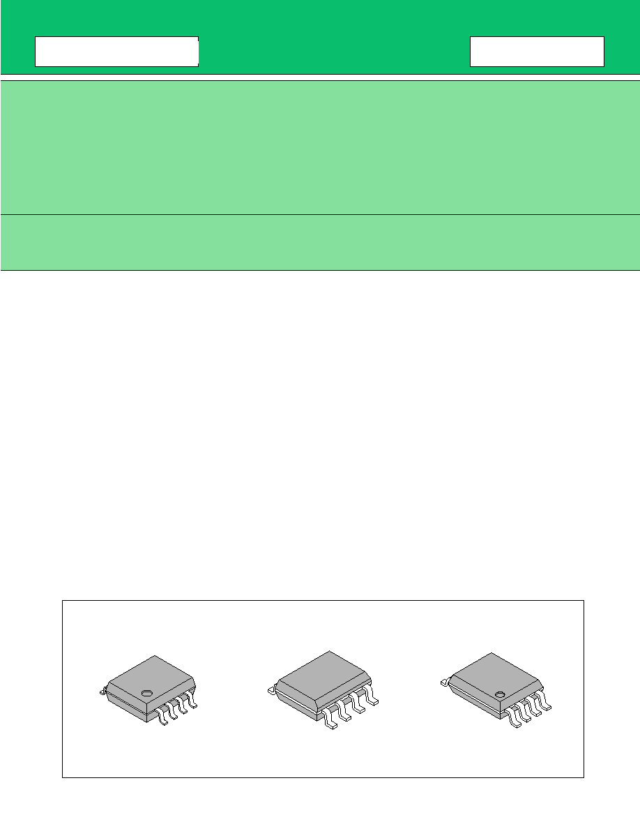
∑ Three types of packages (SOP-8 or SOL-8, SSOP-8)
s
PACKAGES
8-pin Plastic SOP
(FPT-8P-M01
8-pin Plastic SOL
(FPT-8P-M02)
8-pin Plastic SSOP
(FPT-8P-M03)
2
MB3800
s
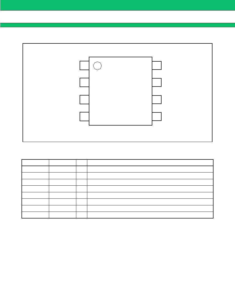
PIN ASSIGNMENT
s
PIN DESCRIPTION
Pin No.
Symbol
I/O
Description
1
≠IN
I
Error amplifier inverting input pin
2
SCP
--
Soft start and SCP setting capacitor connection pin
3
VCC
--
Power supply pin
4
BR/CTL
I
Output current setting and control pin
5
OUT
O
Totem-pole type output pin
6
GND
--
Ground pin
7
OSC
--
Capacitor and resistor connection pin for setting the oscillation frequency
8
FB
O
Error amplifier output pin
2
1
4
3
≠IN
SCP
V
CC
BR/CTL
OSC
FB
OUT
GND
8
7
6
5
(TOP VIEW)
(FPT-8P-M01)
(FPT-8P-M02)
(FPT-8P-M03)
3
MB3800
s
BLOCK DIAGRAM
3
7
6
2
4
5
1
8
0.6 V≠
0.1 V≠
0.1 V
36 k
0.5 V
PWM
Comp.
OUT
≠
+
+
1.25 V
Error Amp.
500
≠
+
≠IN
FB
GND
SCP
BR/CTL
(8 pin)
DTC 0.6 V
0.3 V
30 k
V
CC
OSC
+
Output drive
control circuit
Soft start SCP
Sawtooth wave
oscillator
Reference
voltage supply
4
MB3800
s
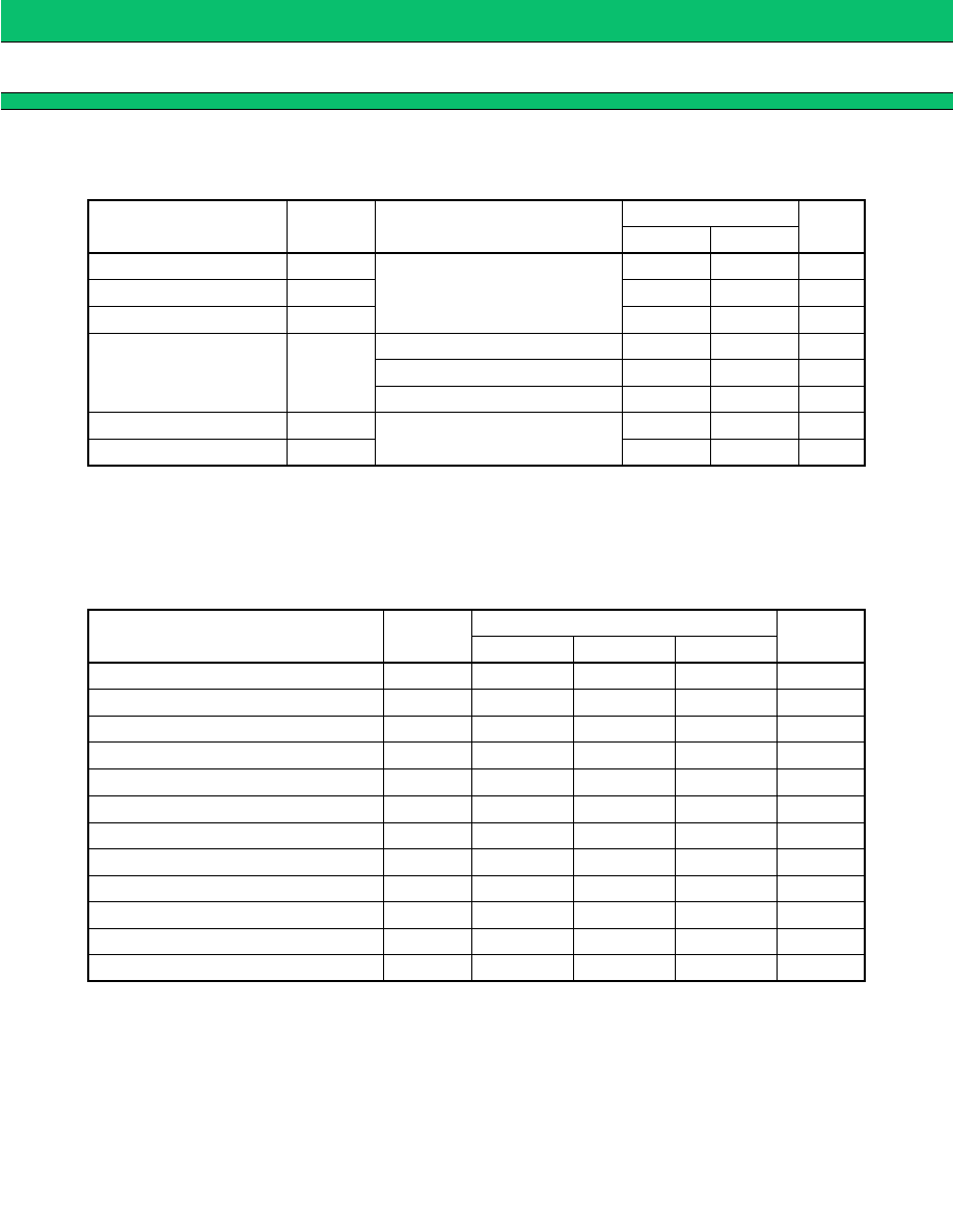
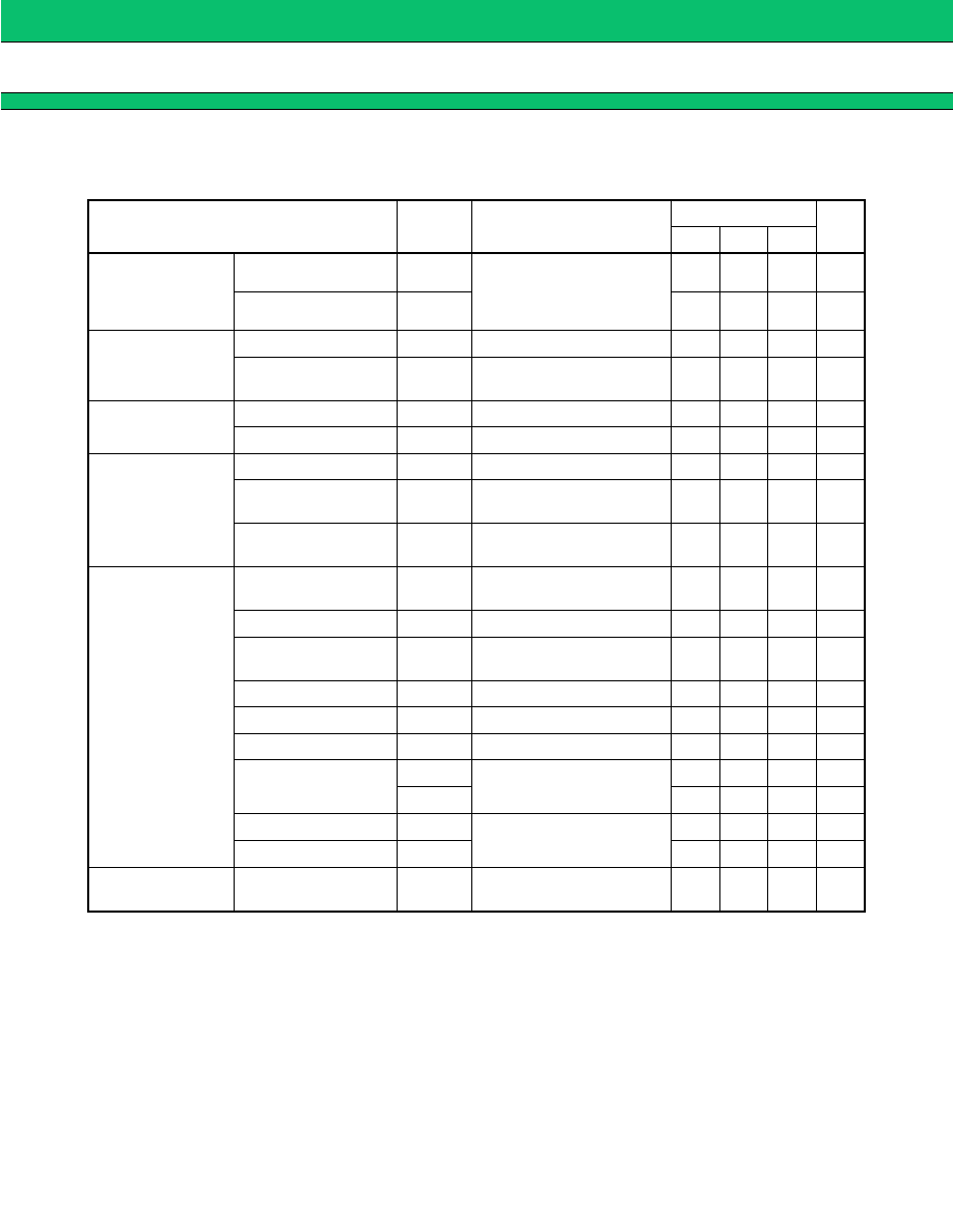
ABSOLUTE MAXIMUM RATINGS
(Ta = +25
∞
C)
* : When mounted on a 10 cm square double-sided epoxy board
WARNING: Semiconductor devices can be permanently damaged by application of stress (voltage, current,
temperature, etc.) in excess of absolute maximum ratings. Do not exceed these ratings.
s
RECOMMENDED OPERATING CONDITIONS
(Ta = +25
∞
C)
WARNING: Recommended operating conditions are normal operating ranges for the semiconductor device. All
the device's electrical characteristics are warranted when operated within these ranges.
Always use semiconductor devices within the recommended operating conditions. Operation outside
these ranges may adversely affect reliability and could result in device failure.
No warranty is made with respect to uses, operating conditions, or combinations not represented on
the data sheet. Users considering application outside the listed conditions are advised to contact their
FUJITSU representative beforehand.
Parameter
Symbol
Condition
Rated Value
Unit
Min.
Max.
Power supply voltage
V
CC
--
--
16
V
Output source current
I
O
+
--
≠50
mA
Output sink current
I
O
≠
--
50
mA
Allowable dissipation
P
D
SOP-8, Ta
+25
∞
C
--
570*
mW
SOP-8, Ta
+25
∞
C
--
430*
mW
SSOP-8, Ta
+25
∞
C
--
580*
mW
Operating temperature
T
op
--
≠30
+85
∞
C
Storage temperature
T
stg
≠55
+125
∞
C
Parameter
Symbol
Values
Unit
Min.
Typ.
Max.
Power supply voltage
V
CC
1.8
--
15
V
Error amplifier input voltage
V
I
≠0.2
--
1.0
V
BR/CTL pin input voltage
V
BR
≠0.2
--
V
CC
V
Output source current
I
O
+
≠40
--
--
mA
Output sink current
I
O
≠
--
--
40
mA
SCP pin capacitance
C
PE
--
0.1
--
µ
F
Phase compensation capacitance
C
P
--
0.1
--
µ
F
Output current setting resistance
R
B
150
390
5000
Timing resistance
R
T
1.0
3.0
10.0
k
Timing capacitance
C
T
100
270
10000
pF
Oscillation frequency
f
OSC
10
500
1000
kHz
Operating temperature
T
OP
≠30
+25
+85
∞
C
5
MB3800
s
ELECTRICAL CHARACTERISTICS
(V
CC
= +2 V, Ta = +25
∞
C)
(Continued)
Parameter
Symbol
Condition
Value
Unit
Min.
Typ.
Max.
Circuit to prevent
malfunction at low
input voltage
(U.V.L.O.)
Reset
voltage V
R
--
--
0.9
V
Threshold voltage
V
TH
1.1
1.3
1.5
V
Soft start
Charging current
I
CS
V
SCP
= 0 V
≠1.5
≠1.0
≠0.7
µ
A
Voltage at soft start
completion
V
tS
--
0.7
0.8
0.9
V
Short circuit
detection (S.C.P.)
Charging current
I
CPC
V
SCP
= 0 V
≠1.5
≠1.0
≠0.7
µ
A
Threshold voltage
V
tPC
--
0.7
0.8
0.9
V
Sawtooth wave
oscillator (OSC)
Oscillation frequency
f
OCS
R
T
= 3.0 k
, C
T
= 270 pF
400
500
600
kHz
Frequency input
stability
f
dV
V
CC
= 2 V to 15 V
--
2
10
%
Frequency variation
with temperature
f
dT
Ta = ≠30∞C to +85∞C
--
5
--
%
Error amplifier
Input threshold
voltage
V
T
V
FB
= 450 mV
480
500
520
mV
V
T
input stability
V
TdV
V
CC
= 2 V to 15 V
--
5
20
mV
V
T
variation with
temperature
V
TdT
Ta = ≠30∞C to +85∞C
--
1
--
%
Input bias current
I
B
V
IN
= 0 V
≠1.0
≠0.2
1.0
µ
A
Voltage gain
A
V
--
70
100
145
V/V
Frequency bandwidth
BW
A
V
= 0 dB
--
6
--
MHz
Maximum output
voltage range
V
OM
+
--
0.78
0.87
--
V
V
OM
≠
--
0.05
0.2
V
Output source current
I
OM
+
V
FB
= 0.45 V
--
≠40
≠24
µ
A
Output sink current
I
OM
≠
24
40
--
µ
A
Idle period
adjustment section
Maximum duty cycle
t
DUTY
R
T
= 3.0 k
, C
T
= 270 pF
V
FB
= 0.8 V
65
75
85
%
--
6
MB3800
(Continued)
s
DIAGRAM
Parameter
Symbol
Condition
Value
Unit
Min.
Typ.
Max.
Output section
Output voltage
V
OH1
R
B
= 390
, I
O
= ≠15 mA
1.0
1.2
--
V
V
OH2
R
B
= 750
, V
CC
= 1.8 V
I
O
= ≠10 mA
0.8
1.0
--
V
V
OL1
R
B
= 390
, I
O
= 15 mA
--
0.1
0.2
V
V
OL2
R
B
= 750
, V
CC
= 1.8 V
I
O
= 10 mA
--
0.1
0.2
V
Output source current
I
O
+
R
B
= 390
, V
O
= 0.9 V
--
≠30
≠20
mA
Output sink current
I
O
≠
R
B
= 390
, V
O
= 0.3 V
30
60
--
mA
Pull down resistance
R
O
--
20
30
40
k
Output current
setting section/
Control section
Pin voltage
V
BR
R
B
= 390
0.2
0.3
0.4
V
Input off condition
I
OFF
--
≠20
--
0
µ
A
Input on condition
I
ON
--
--
≠45
µ
A
Pin current range
I
BR
≠1.8
--
≠0.1
mA
Entire device
Stand-by current
I
CCS
BR/CTL pin open or V
CC
--
--
1
µ
A
Average supply
current
I
CC
R
B
= 390
--
5.5
9.3
mA
t
S
t
PE
ON
OFF
FB pin voltage
Reference input for short circuit
detection comparator
Idle period setting voltage
Sawtooth wave output
Soft start setting voltage
OUT pin waveforms
SCP pin waveforms
Power supply control SW
Soft start
Output
short
circuit
Output short circuit
Short circuit
detection

7
MB3800
s
HOW TO SET THE TIME CONSTANT FOR SOFT START AND SHORT CIRCUIT
DETECTION
1.
Soft Start
At power on, the capacitor C
PE
connected to the SCP pin starts charging. The PWM comparator compares the soft
start setting voltage as a proportion of the voltage at the SCP pin with the sawtooth waveform. The comparison
controls the ON duty of the OUT pin, causing the soft start operation. On completion of soft start operation, the
voltage at the SCP pin stays low, the soft start setting voltage stays high, and the circuit enters the output short
circuit detection wait state.
Soft start time (The time until the output ON duty reaches approximately 50%)
t
S
[s]
0.35
◊
C
PE
[
µ
F]
2.
Short Circuit Protection
If the switching regulator output suddenly drops due to load effect, the error amplifier output (FB pin) is fixed at
VOM
+
and capacitor C
PE
starts charging. When the voltage at the SCP pin reaches approximately 0.8V, the output
pin is set low and the SCP pin stays low.
Once the protection circuit operates, the circuit can be restored by resetting the power supply.
∑ Short circuit detection time
t
PE
[s]
0.8
◊
C
PE
[
µ
F]
8
MB3800
s
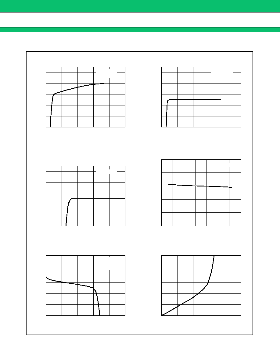
TYPICAL CHARACTERISTICS
(Continued)
10
8
6
4
2
0
4
8
12
16
20
Supply voltage V
CC
(V)
Supply current I
CC
(mA)
1.0
0.8
0.6
0.4
0.2
0
4
8
12
16
20
Supply voltage V
CC
(V)
Input threshold voltage V
T
(V)
Supply voltage vs. Input threshold voltage
T
a
= +25
∞
C
10
5
0
≠10
80
100
Ambient temperature T
a
(
∞
C)
Input threshold voltage variation ratio
V
T
/V
T
(%)
Ambient temperature vs. Input threshold
voltage variation ratio
V
CC
= 2 V
1.0
0.8
0.6
0.4
0.2
0
0
2.0
3.0
4.0
5.0
Supply voltage V
CC
(V)
Input threshold voltage V
T
(V)
Supply voltage vs. Input threshold voltage
T
a
= +25
∞
C
40
60
0
20
≠40
≠20
≠5
2.0
1.6
1.2
0.8
0.4
≠10
≠20
≠30
≠40
≠50
High level output current I
OUT
(mA)
High level output voltage V
OUT
(V)
High level output
V
CC
= 2 V
R
B
= 390
T
a
= +25
∞
C
500
400
300
200
100
20
40
60
80
100
High level output current I
OUT
(mA)
Low level output voltage V
OUT
(mV)
Low level output
V
CC
= 2 V
R
B
= 390
T
a
= +25
∞
C
0
0
0
0
T
a
= +25
∞
C
R
B
= 390
0
0
1.0
≠15
Supply voltage vs. Supply current
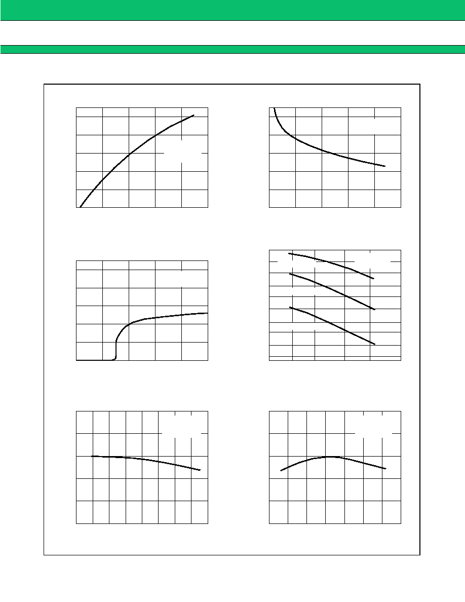
9
MB3800
(Continued)
(Continued)
≠10
≠0.4
BR/CTL pin current I
BR
(mA)
Output source current I
OUT
(mA)
BR/CTL pin current vs. Output source current
0
0
≠0.8
≠1.2
≠1.6
≠2.0
≠20
≠30
≠40
≠50
V
CC
= 2 V
V
OUT
= 0.9 V
T
a
= +25
∞
C
100
≠0.4
BR/CTL pin current I
BR
(mA)
BR/CTL pin voltage V
BR
(mV)
BR/CTL pin current vs. BR/CTL pin voltage
0
0
≠0.8
≠1.2
≠1.6
≠2.0
200
300
400
500
V
CC
= 2 V
T
a
= +25
∞
C
1.0
≠20
BR/CTL pin current I
BR
(
µ
A)
Supply current I
CC
(mA)
BR/CTL pin current vs. Supply current
0
0
≠40
≠60
≠80
≠100
2.0
3.0
4.0
5.0
V
CC
= 2 V
T
a
= +25
∞
C
1 k
Timing resistor R
T
(
)
Oscillation frequency f
OSC
(Hz)
Timing resistor vs. Oscillation frequency
10 k
2 k
50 k
500 k
2
Supply voltage V
CC
(V)
Frequency variation ratio
f/f (%)
Supply voltage vs. Frequency variation ratio
≠15
0
5
10
≠5
0
≠10
4
6
8
10
12
14
16
C
T
= 270 pF
R
T
= 3.0 k
T
a
= +25
∞
C
≠20
Ambient temperature T
a
(
∞
C)
Frequency variation ratio
f/f (%)
Ambient temperature vs. Frequency variation ratio
≠15
≠40
5
10
≠5
0
≠10
0
20
40
60
80
100
V
CC
= 2 V
C
T
= 270 pF
R
T
= 3.0 k
5 k
20 k
200 k
5 k
2 k
10 k
100 k
1 M
20 k
C
T
= 100 pF
C
T
= 1000 pF
C
T
= 10000 pF
V
CC
= 2 V
T
a
= +25
∞
C
10
MB3800
(Continued)
Oscillation frequency f
OSC
(Hz)
Maximum duty cycle t
DUTY
(%)
Oscillation frequency vs. Maximum duty cycle
0
10 K
100
40
60
20
100 K
1 M
80
0
0.4
0.8
1.2
1.6
2.0
t
(
µ
s)
≠50
0
50
0
2
4
6
(V)
(mA)
V
OUT
I
OUT
2 V
10 mV
200 ns
V
CC
= 2 V
C
T
= 270 pF
R
T
= 1.0 k
18 k
2 k
10
µ
F
I
OUT
(5 V)
390
V
OUT
22
µ
H
V
CC
MB3800
5
4
≠IN
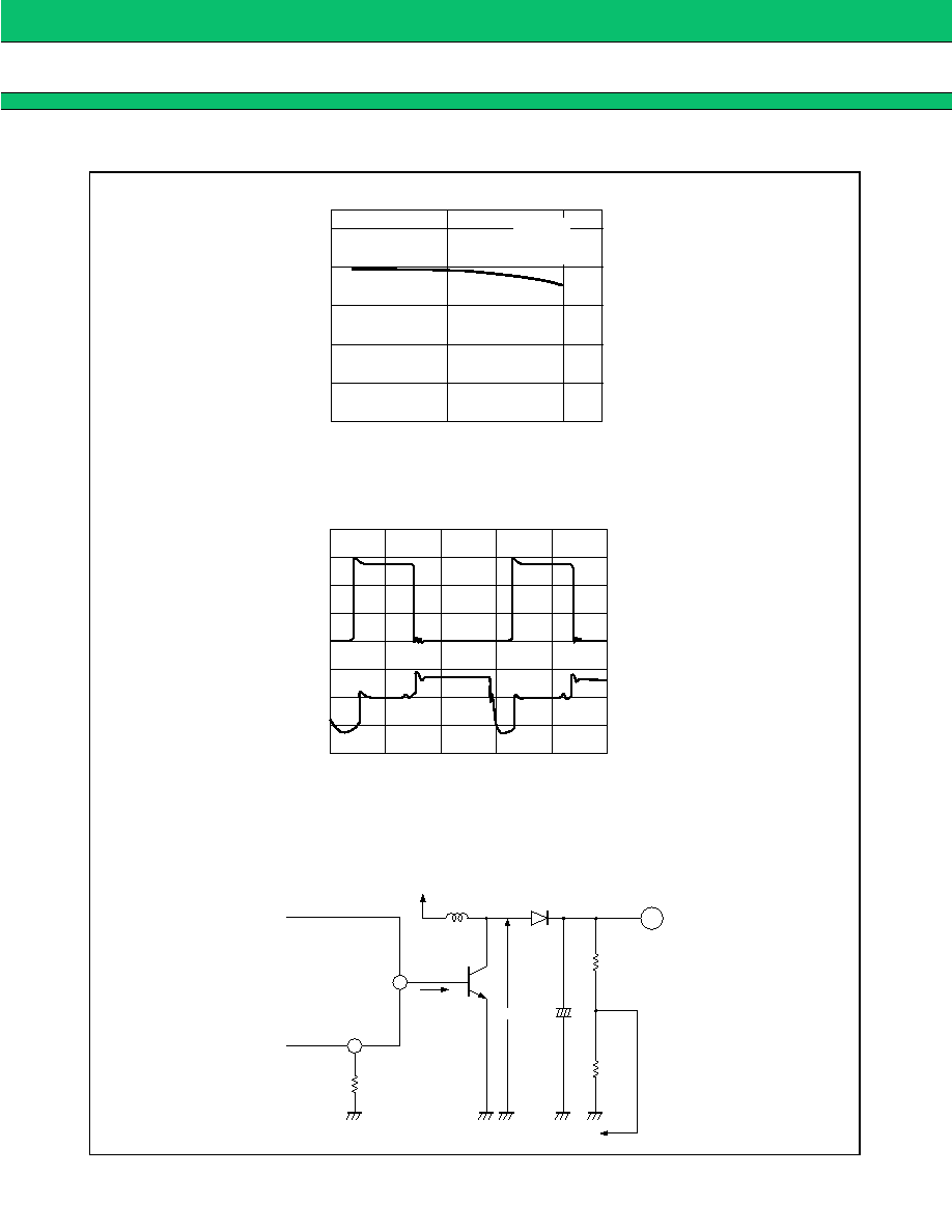
Output pin voltage and current waveforms
(reference data)
Note: The OFF delay time of V
OUT
depends on the
characteristics of the external transistor.
Measurement circuit diagram
V
CC
= 2 V
C
T
= 270 pF
T
a
= +25
∞
C
11
MB3800
s
FUNCTIONAL DESCRIPTION
1.
Switching Regulator Function
(1) Reference voltage circuit
The reference voltage circuit generates a temperature-compensated reference voltage (
1.25V) from voltage
supplied from the power supply pin (pin 3). In addition to providing the reference voltage for the switching regulator,
the circuit also sets the idle period.
(2) Sawtooth wave oscillator
The sawtooth oscillator generates a sawtooth wave (up to 1 MHz) that is stable with respect to the supply voltage
and temperature. The capacitor and resistor that set the oscillation frequency are connected to the OSC pin (pin 7).
(3) Error amplifier (Error Amp.)
The error amplifier detects the output voltage of the switching regulator and outputs the PWM control signal. The
voltage gain is fixed, and connecting a phase compensation capacitor to the FB pin (pin 8) provides stable phase
compensation for the system.
(4) PWM comparator (PWM Comp.)
The voltage comparator has one inverting and three non-inverting inputs. The comparator is a voltage/pulse width
converter that controls the ON time of the output pulse depending on the input voltage. The output level is high (H)
when the sawtooth wave is lower than the error amplifier output voltage, soft start setting voltage, and idle period
setting voltage.
(5) Output circuit
The output circuit has a totem pole type configuration and can drive an external NPN transistor directly. The value
of the ON/OFF current can be set by a resistor connected to the BR/CTL pin (pin 4).
2.
Power Supply Control Function
Stand-by mode (supply current 1
µ
A or less) can be set by connecting the BR/CTL pin (pin 4) to V
CC
or by making
the pin open circuit.
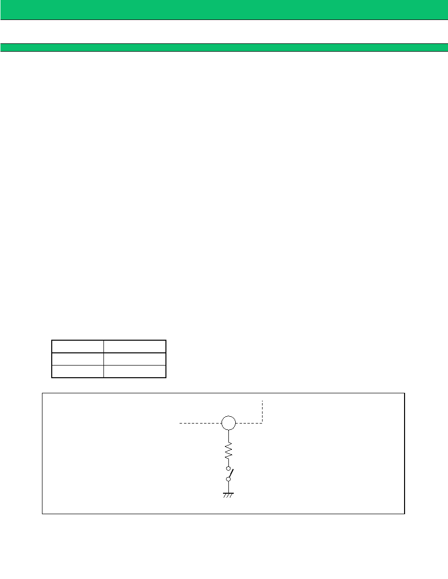
SW
Mode
OFF
Stand-by mode
ON
Operating mode
RB
SW
4
BR/CTL
MB3800
12
MB3800
3.
Other Functions
(1) Soft start and short circuit detection
Soft start operation is set by connecting capacitor C
PE
to the SCP pin (pin 2). Soft start prevents a current spike on
start-up.
On completion of soft start operation, the SCP pin (pin 2) stays low and enters the short circuit detection wait state.
When an output short circuit occurs, the error amplifier output is fixed at V
OM
+ and capacitor C
PE
starts charging.
After charging to approximately 0.8 V, the output pin (pin 5) is set low and the SCP pin (pin 2) stays low.
Once the protection circuit operates, the circuit can be restored by resetting the power supply. (See "
s
HOW TO
SET THE TIME CONSTANT FOR SOFT START AND SHORT CIRCUIT DETECTION".)
(2) Circuit to prevent malfunction at low input voltage
Transients when powering on or instantaneous glitches in the supply voltage can lead to malfunction of the control
IC and cause system damage or failure. The circuit to prevent malfunction at low input voltage detects a low input
voltage by comparing the supply voltage to the internal reference voltage. On detection, the circuit fixes the output
pin to low.
The system recovers when the supply voltage rises back above the threshold voltage of the malfunction prevention
circuit.
s
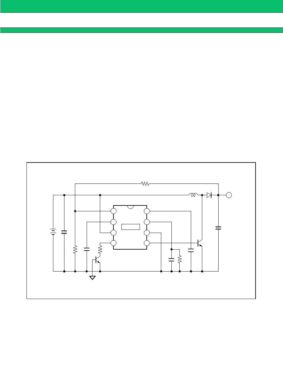
APPLICATION EXAMPLE
1
2
4
3
8
7
6
5
MB3800
3 k
22
µ
H
10
µ
F
270 pF
0.1
µ
F
18 k
V o
(5 V)
2 k
0.1
µ
F
390
CTL
33
µ
F
V in
(3 V)
FB
OSC
GND
OUT
≠IN
SCP
V
CC
BR/CTL

13
MB3800
s
USAGE PRECAUTIONS
1.
Do not apply an input voltage greater than the maximum rating.
Do not input voltages greater than the maximum rating as this can cause damage to the LSI.
2.
Use in accordance with the recommended operating conditions.
The electrical characteristics of the LSI are not guaranteed if the input voltage is greater than the maximum. Also,
LSI operation is unstable if the input voltage is less than the minimum. Therefore, always use in accordance with
the recommended operating conditions.
3.
Use a wide ground line on the printed circuit board.
As the LSI uses a high frequency and therefore can generate high frequency noise, make the ground line as wide
as possible.
4.
Take anti-static precautions.
∑ Use a holder for inserting the semiconductor which is anti-static or conductive.
∑ After mounting the device on a printed circuit board, store or transport the board in a conductive bag or
container.
∑ Earth work benches, tools, and measuring equipment.
∑ Ensure that maintenance personnel have a resistance of 250 k
to 1 M
in series between their body and earth.

14
MB3800
s
ORDERING INFORMATION
Part number
Package
Remarks
MB3800PF
8-pin Plastic SOP
(FPT-8P-M01)
MB3800PNF
8-pin Plastic SOL
(FPT-8P-M02)
MB3800PFV
8-pin Plastic SSOP
(FPT-8P-M03)
15
MB3800
s
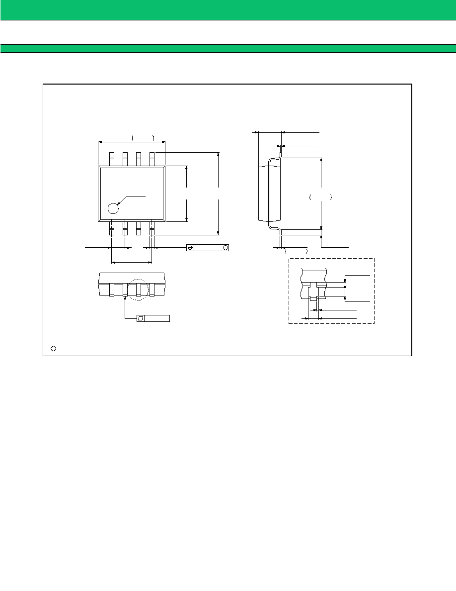
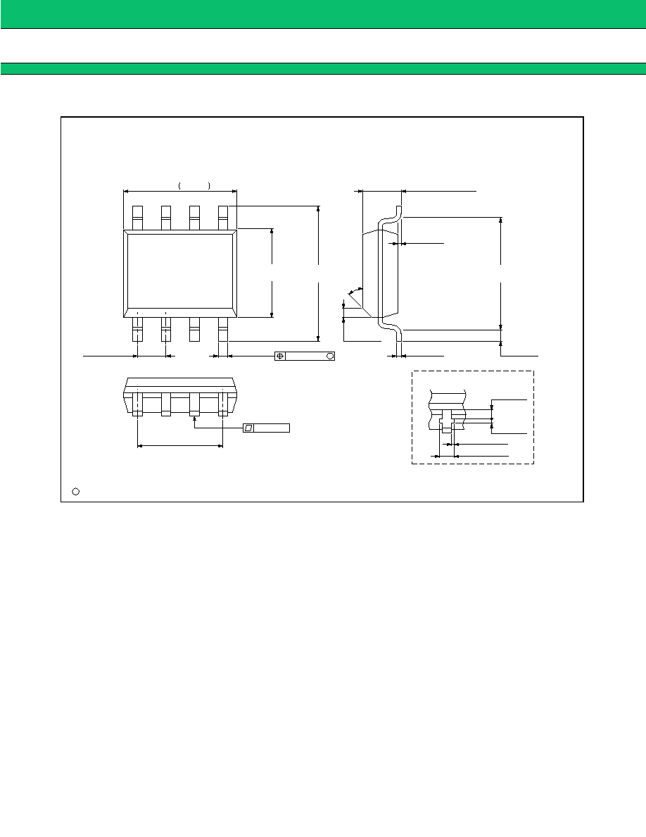
PACKAGE DIMENSIONS
(Continued)
8-pin Plastic SOP
(FPT-8P-M01)
+0.40
≠0.20
+.016
≠.008
+0.05
≠0.02
+.002
≠.001
+0.25
≠0.20
+.010
≠.008
3.81(.150)REF
1.27(.050)
TYP
INDEX
6.80
.268
0.15
.006
6.35
.250
(.307±.016)
(.209±.012)
(.018±.004)
(STAND OFF)
(.020±.008)
0.50±0.20
5.30±0.30
7.80±0.40
0.05(.002)MIN
2.25(.089)MAX
0.45±0.10
Details of "A" part
0.50(.020)
0.20(.008)
0.18(.007)MAX
0.68(.027)MAX
"A"
M
ÿ0.13(.005)
0.10(.004)
1994 FUJITSU LIMITED F08002S-4C-4
C
Dimensions in mm (inches).
16
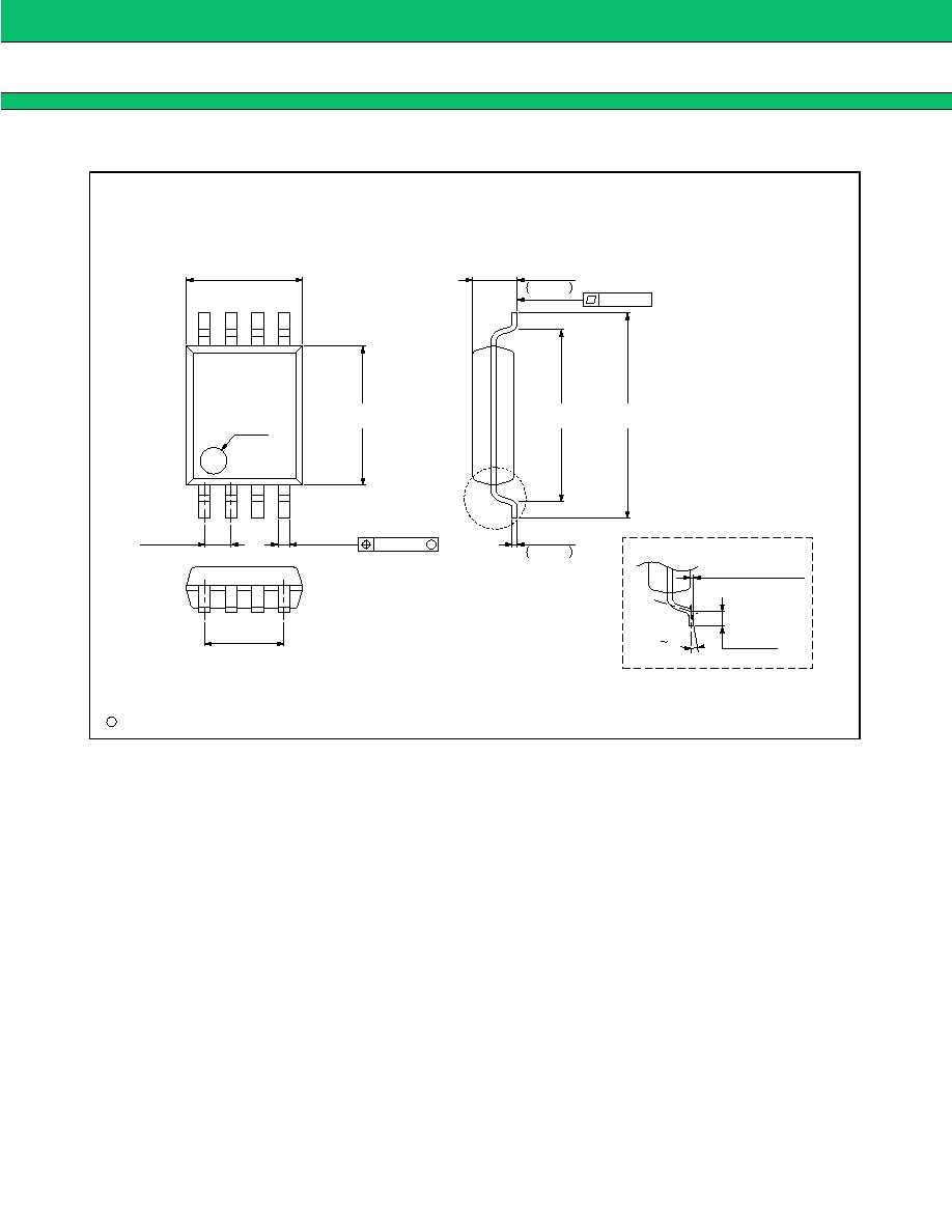
MB3800
(Continued)
8-pin Plastic SOL
(FPT-8P-M02)
+0.25
≠0.20
+.010
≠.008
45∞
(STAND OFF)
(.020±.008)
Details of "A" part
0.20(.008)
0.40(.016)
0.18(.007)MAX
0.65(.026)MAX
"A"
(.006±.004)
(.197±.012)
(.236±.016)
(.154±.012)
(.008±.002)
(.017±.004)
M
ÿ0.13(.005)
0.10(.004)
5.05
.199
3.81(.150)REF
0.40(.016)
5.00±0.30
0.50±.020
6.00±0.40
3.90±0.30
0.15±0.10
1.55±0.20(.061±.008)
0.20±0.05
0.42±0.10
1.27(.050)TYP
1994 FUJITSU LIMITED F08004S-2C-4
C
Dimensions in mm (inches).
17
MB3800
(Continued)
8-pin Plastic SSOP
(FPT-8P-M03)
+0.05
≠0.02
+.002
≠.001
+0.20
≠0.10
+.008
≠.004
Details of "A" part
0 10∞
(STAND OFF)
0.10±0.10(.004±.004)
(.020±.008)
0.50±0.20
0.80(.0315)
TYP
*
INDEX
"A"
0.10(.004)
0.15
.006
1.25
.049
M
0.10(.004)
(.165±.004)
(.244±.008)
NOM
(.014±.004)
(.138±.004)
6.20±0.20
5.20(.205)
4.20±0.10
2.40(.094)REF
0.35±0.10
3.50±0.10
1994 FUJITSU LIMITED F08005S-1C-2
C
Dimensions in mm (inches).

18
MB3800
FUJITSU LIMITED
For further information please contact:
Japan
FUJITSU LIMITED
Corporate Global Business Support Division
Electronic Devices
KAWASAKI PLANT, 4-1-1, Kamikodanaka
Nakahara-ku, Kawasaki-shi
Kanagawa 211-8588, Japan
Tel: (044) 754-3763
Fax: (044) 754-3329
http://www.fujitsu.co.jp/
North and South America
FUJITSU MICROELECTRONICS, INC.
Semiconductor Division
3545 North First Street
San Jose, CA 95134-1804, USA
Tel: (408) 922-9000
Fax: (408) 922-9179
Customer Response Center
Mon. - Fri.: 7 am - 5 pm (PST)
Tel: (800) 866-8608
Fax: (408) 922-9179
http://www.fujitsumicro.com/
Europe
FUJITSU MIKROELEKTRONIK GmbH
Am Siebenstein 6-10
D-63303 Dreieich-Buchschlag
Germany
Tel: (06103) 690-0
Fax: (06103) 690-122
http://www.fujitsu-ede.com/
Asia Pacific
FUJITSU MICROELECTRONICS ASIA PTE LTD
#05-08, 151 Lorong Chuan
New Tech Park
Singapore 556741
Tel: (65) 281-0770
Fax: (65) 281-0220
http://www.fmap.com.sg/
F9802
©
FUJITSU LIMITED Printed in Japan
All Rights Reserved.
The contents of this document are subject to change without
notice. Customers are advised to consult with FUJITSU sales
representatives before ordering.
The information and circuit diagrams in this document presented
as examples of semiconductor device applications, and are not
intended to be incorporated in devices for actual use. Also,
FUJITSU is unable to assume responsibility for infringement of
any patent rights or other rights of third parties arising from the
use of this information or circuit diagrams.
FUJITSU semiconductor devices are intended for use in
standard applications (computers, office automation and other
office equipment, industrial, communications, and measurement
equipment, personal or household devices, etc.).
CAUTION:
Customers considering the use of our products in special
applications where failure or abnormal operation may directly
affect human lives or cause physical injury or property damage,
or where extremely high levels of reliability are demanded (such
as aerospace systems, atomic energy controls, sea floor
repeaters, vehicle operating controls, medical devices for life
support, etc.) are requested to consult with FUJITSU sales
representatives before such use. The company will not be
responsible for damages arising from such use without prior
approval.
Any semiconductor devices have inherently a certain rate of
failure. You must protect against injury, damage or loss from
such failures by incorporating safety design measures into your
facility and equipment such as redundancy, fire protection, and
prevention of over-current levels and other abnormal operating
conditions.
If any products described in this document represent goods or
technologies subject to certain restrictions on export under the
Foreign Exchange and Foreign Trade Control Law of Japan, the
prior authorization by Japanese government should be required
for export of those products from Japan.