 | –≠–ª–µ–∫—Ç—Ä–æ–Ω–Ω—ã–π –∫–æ–º–ø–æ–Ω–µ–Ω—Ç: MB3825 | –°–∫–∞—á–∞—Ç—å:  PDF PDF  ZIP ZIP |
DS04-27220-2E
FUJITSU SEMICONDUCTOR
DATA SHEET
ASSP For Power Supply Applications
6-ch DC/DC Converter IC With Synchronous Rectifier
MB3825A
s
DESCRIPTION
The MB3825A is a pulse width modulation (PWM) type 6-channel DC/DC converter IC with synchronous rectification
(2-channels) designed for low voltage, high efficiency operation in high precision and high frequency applications,
ideal for down conversion.
The MB3825A is an ideal device offering low power consumption, compact size and light weight for products such
as self-contained camcorders and digital still cameras.
s
FEATURES
∑ Synchronous rectification (channels 1 and 4)
∑ High efficiency drive with power-on output enhanced by built-in speed-up circuit
∑ Wide range of operating power supply voltage : 2.5 V to 12 V
∑ Built-in high-precision reference voltage generator : 1.5 V±1%
∑ Wide operating oscillator frequency range, high frequency capability : 50 kHz to 800 kHz
∑ Wide input voltage range (all channels) : 0 V to Vcc - 0.9 V
∑ Error amplifier output for soft start (channels 1, 2, 4) (All channels may be set for same soft start time regardless
of duty factor setting.)
s
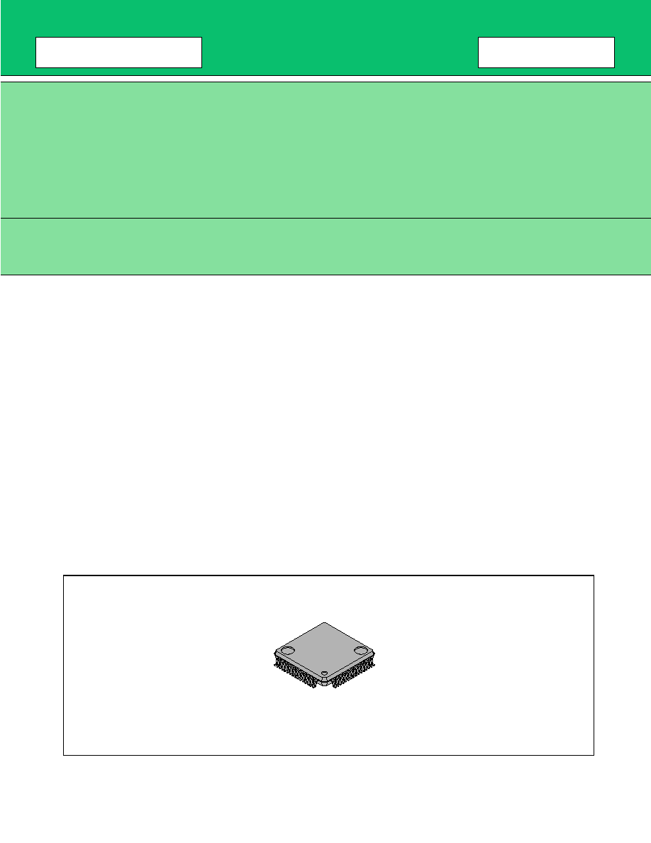
PACKAGE
64-pin, Plastic LQFP
(FPT-64P-M03)
MB3825A
2
s
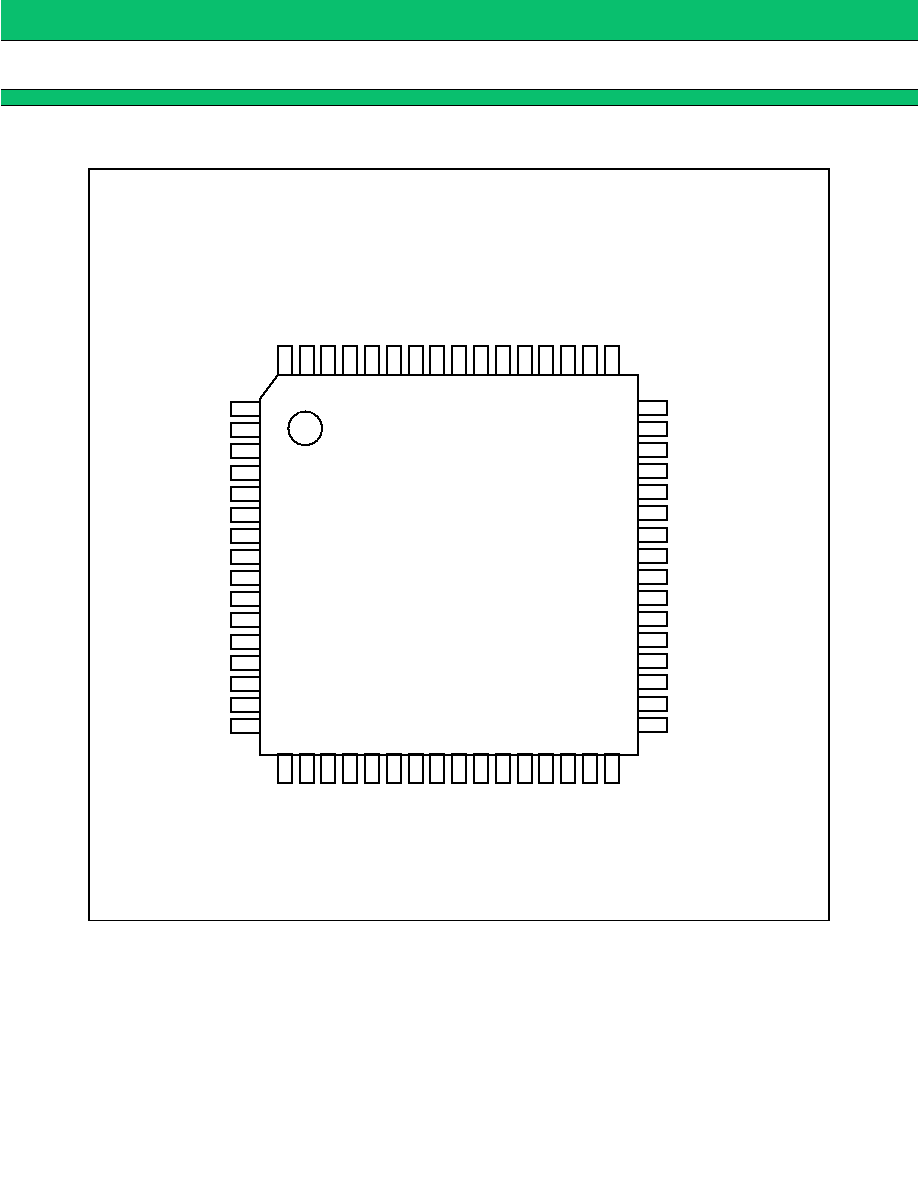
PIN ASSIGNMENT
1
2
3
4
5
6
7
8
9
10
11
12
13
14
15
16
CB2-5
CB1-5
VB5
OUT1-6
CB2-6
CB1-6
VB6
OVP5
,
6
IN (C) 6
+
IN (E) 6
-
IN (E) 6
FB6
SCP
IN (C) 5
+
IN (E) 5
-
IN (E) 5
48
47
46
45
44
43
42
41
40
39
38
37
36
35
34
33
CB1-2
VB2
OUT1-1
CB2-1
CB1-1
OUT2-1
VCC (O) 1
,
3
VB1
IN (C) 1
-
IN (E) 1
FB1
IN (C) 2
-
IN (E) 2
FB2
IN (C) 3
-
IN (E) 3
64
63
62
61
60
59
58
57
56
55
54
53
52
51
50
49
OUT1-5
VCC (O) 4
,
5
,
6
VB4
GND (O) 4
,
5
,
6
OUT2-4
CB1-4
CB2-4
OUT1-4
OUT1-3
CB2-3
CB1-3
GND (O) 1
,
2
,
3
VB3
VCC (O) 2
OUT1-2
CB2-2
17
18
19
20
21
22
23
24
25
26
27
28
29
30
31
32
FB5
IN (C) 4
-
IN (E) 4
FB4
RT
CT
CSCP
GND1
GND2
CS
VREF
VCC
CTL2
CTL1
DTC3
FB3
MB3825A
3
s
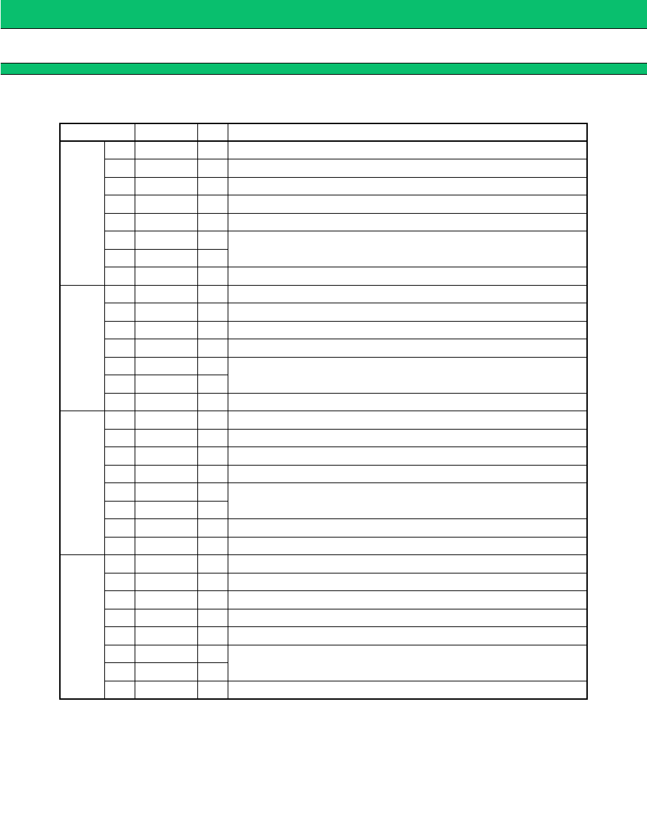
PIN DESCRIPTION
(Continued)
Pin No.
Symbol
I/O
Descriptions
CH 1
38
FB1
O
Channel 1 error amplifier output pin.
39
≠IN(E)1
I
Channel 1 error amplifier inverted input pin.
40
IN(C)1
I
Channel 1 short detection comparator input pin.
46
OUT1-1
O
Channel 1 main side output pin.
43
OUT2-1
O
Channel 1 synchronous rectifier side output pin.
44
CB1-1
--
Channel 1 boot capacitor connection pin.
45
CB2-1
--
41
VB1
--
Channel 1 output sink current setting pin.
CH 2
35
FB2
O
Channel 2 error amplifier output pin.
36
≠IN(E)2
I
Channel 2 error amplifier inverted input pin.
37
IN(C)2
I
Channel 2 short detection comparator input pin.
50
OUT1-2
O
Channel 2 output pin.
48
CB1-2
--
Channel 2 boot capacitor connection pin.
49
CB2-2
--
47
VB2
--
Channel 2 output sink current setting pin.
CH 3
32
FB3
O
Channel 3 error amplifier output pin.
33
≠IN(E)3
I
Channel 3 error amplifier inverted input pin.
34
IN(C)3
I
Channel 3 short detection comparator input pin.
56
OUT1-3
O
Channel 3 output pin.
54
CB1-3
--
Channel 3 boot capacitor connection pin.
55
CB2-3
--
52
VB3
--
Channel 3 output sink current setting pin.
31
DTC3
I
Channel 3 dead time control pin.
CH 4
20
FB4
O
Channel 4 error amplifier output pin.
19
≠IN(E)4
I
Channel 4 error amplifier inverted input pin.
18
IN(C)4
I
Channel 4 short detection comparator input pin.
57
OUT1-4
O
Channel 4 main side output pin.
60
OUT2-4
O
Channel 4 synchronous rectifier side output pin.
59
CB1-4
--
Channel 4 boot capacitor connection pin.
58
CB2-4
--
62
VB4
--
Channel 4 output sink current setting pin.
MB3825A
4
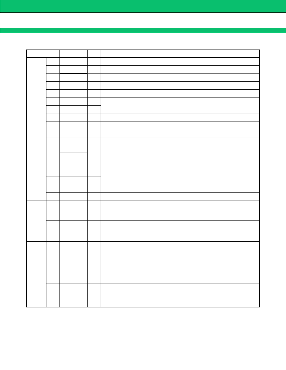
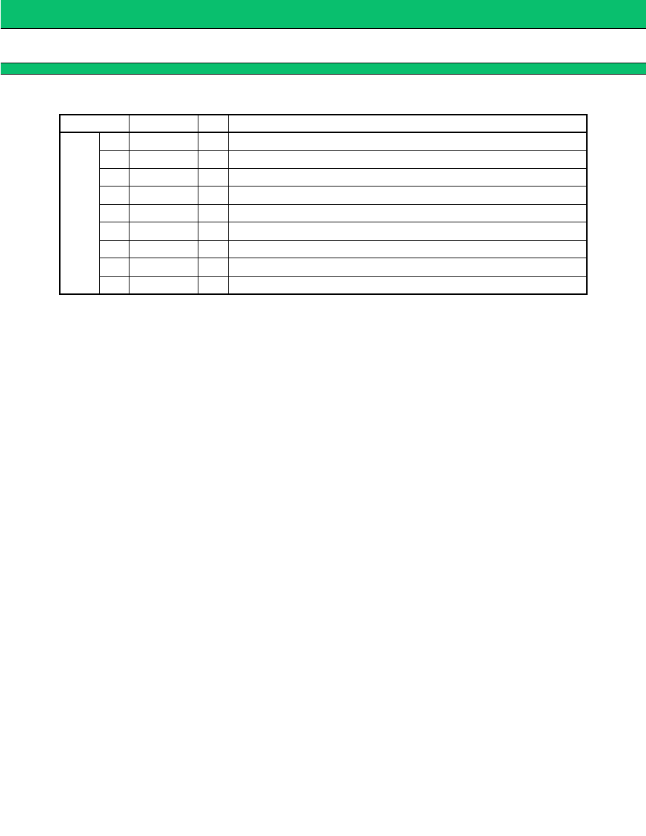
(Continued)
(Continued)
Pin No.
Symbol
I/O
Descriptions
CH 5
17
FB5
O
Channel 5 error amplifier output pin.
16
≠IN(E)5
I
Channel 5 error amplifier inverted input pin.
15
+IN(E)5
I
Channel 5 error amplifier non-inverted input pin.
14
IN(C)5
I
Channel 5 short detection comparator input pin.
64
OUT1-5
O
Channel 5 output pin.
2
CB1-5
--
Channel 5 boot capacitor connection pin.
1
CB2-5
--
3
VB5
--
Channel 5 output sink current setting pin.
8
OVP5,6
I
Channel 5, 6 output maximum voltage setting pin.
CH 6
12
FB6
O
Channel 6 error amplifier output pin.
11
≠IN(E)6
I
Channel 6 error amplifier inverted input pin.
10
+IN(E)6
I
Channel 6 error amplifier non-inverted input pin.
9
IN(C)6
I
Channel 6 short detection comparator input pin.
4
OUT1-6
O
Channel 6 output pin.
6
CB1-6
--
Channel 6 boot capacitor connection pin.
5
CB2-6
--
7
VB6
--
Channel 6 output sink current setting pin.
8
OVP5,6
I
Channel 5, 6 output maximum voltage setting pin.
21
RT
--
Triangular wave frequency setting resistor connection pin.
22
CT
--
Triangular wave frequency setting capacitor connection pin.
30
CTL1
I
Power supply control circuit.
"H" level: Power supply operating mode
"L" level: Standby mode
29
CTL2
I
Channel 3 control circuit.
When CTL1 pin is "H" level
"H" level: Channel 3 in operating mode
"L" level: Channel 3 in OFF mode
13
SCP
I
Short detection comparator input pin.
23
CSCP
--
Short protection circuit capacitor connection pin.
26
CS
--
Soft start circuit capacitor connection pin.
Triangular-Wave
Oscil
l
ator
Circuit
Control
Circuit
MB3825A
5
(Continued)
Pin No.
Symbol
I/O
Description
28
VCC
--
Reference voltage and control circuit power supply pin.
42
VCC(O)1,3
--
Output circuit power supply pin (Channel 1, 3).
51
VCC(O)2
--
Output circuit power supply pin (Channel 2).
63
VCC(O)4,5,6
--
Output circuit power supply pin (Channel 4,5,6).
27
VREF
O
Reference voltage output pin.
24
GND1
--
Ground pin.
25
GND2
--
Ground pin.
53
GND(O)1,2,3
--
Output circuit ground pin (Channel 1,2,3).
61
GND(O)4,5,6
--
Output circuit ground pin (Channel 4,5,6).
Power Supply
Circuit